Note: Descriptions are shown in the official language in which they were submitted.
CA 02913679 2015-11-30
1
IMPROVEMENTS IN OR RELATING TO LENS ARRAYS
Field of the invention
The present invention relates to improvements in or relating to
lens arrays, and is more particularly concerned with the mounting of such
lens arrays with respect to light-emitting diode elements mounted on a
printed circuit board.
Background of the invention
Light emitting diode (LED) based luminaires often comprise
modules including printed circuit boards (PCBs) on which the LEDs are
mounted. The LEDs are typically arranged in an array or pattern and
mounted on the PCB, often termed PCB assembly (PCBA), which is
appropriate for the luminaire in which they are to be used. Whilst each LED
comprises a light source with a primary optical element or lens, secondary
optical elements are often required to direct the light produced by these
light
sources in directions appropriate to the particular implementation in a
luminaire. Lenses are typically used as the secondary optical elements for
directing the light.
In current applications, most secondary lenses are made out of
rather rigid materials, such as polymethylmethacrylate (PMMA) or
polycarbonate, and are mounted on the PC BA by the use of screws or rivets
which provide precise positioning of the secondary lenses with respect to the
associated LEDs.
Unfortunately, the use of PMMA or polycarbonate lenses as
secondary lenses tends to limit the operating temperature of the PCBA.
Conventional plastic materials such as PMMA and polycarbonate cannot be
exposed to temperatures exceeding 85 C without long term deterioration, for
CA 02913679 2015-11-30
t.
2
example, due to thermo-oxidation. The LEDs and PCBAs, particularly when
they comprise metal core PCBs (MCPCBs), are more resistant to higher
temperatures, and, the material from which the secondary lenses are most
often made limits the maximum operable temperature of the assembly. This
limitation in temperature necessitates the provision of good dissipation
techniques on the luminaire to keep the temperatures under this limit. This
requires costly heat dissipating structures, for example, heat sinks which
increase the amount of metal, for example, aluminium, required in the
manufacture of the luminaire housing or body in which the LEDs are
mounted.
Silicone is now being implemented in more and more
applications as secondary lenses for use with PBCAs as it can operate at
higher temperatures than PMMA and polycarbonate without significant
degradation of the material, whilst providing optical properties that remain
consistent over extended periods of time. Silicone is a proven material for
use in encapsulated LED primary lenses due to its ability to operate at
higher temperatures.
However, when implementing silicone as a single moulded lens
array, it becomes difficult to mount the array precisely on the PCBA and to
maintain precise alignment between the secondary lenses and the LEDs.
This is due to silicone itself being a soft material and the moulded lens
array
is flexible. More particularly, due to the relative softness and flexibility
of the
material, it is no longer possible to use conventional mounting techniques,
for example, using screws, rivets, etc.
Furthermore, the goal of achieving higher operating
temperatures generates even more severe constraints due to different
thermal characteristics of the materials from which the secondary lenses and
PCBA are made. These characteristics need to be taken into account to
CA 02913679 2015-11-30
3
provide a reliable mounting of the lenses whilst also maintaining correct lens
alignment with respect to the LEDs during temperature changes.
Summary of the invention
It is therefore an object of the present invention to provide a
method of providing precise alignment between a moulded secondary lens
array made of a soft, flexible material and an array of LED elements
mounted on a printed circuit board.
It is another object of the present invention to provide a method
of attaching a moulded secondary lens array to a printed circuit board which
provides precision of mounting in three-dimensions.
It is a further object of the present invention to provide means
for attaching a moulded secondary lens array with precision which does not
require any tools.
It is yet another object of the present invention to provide
means for compensating for different thermal characteristics of the
components in an LED module.
In accordance with one aspect of the present invention, there is
provided a light-emitting diode module comprising:-
a printed circuit board having a first surface and a second
surface;
a light-emitting diode array mounted on first surface of the
printed circuit board, the printed circuit board providing electrical
connections
to each light-emitting diode element in the light-emitting diode array; and
a secondary lens array operable for being positioned over the
light-emitting diode array, the secondary lens array including a secondary
lens element for each light-emitting diode element in the light-emitting diode
array;
CA 02913679 2015-11-30
4
characterised in that the module further comprises a lens
holder mountable to the printed circuit board and operable for retaining each
secondary lens element of the secondary lens array in alignment in an x-y
plane with respect to each light-emitting diode element of the light-emitting
diode array and for maintaining the secondary lens array at a predetermined
distance, in a direction perpendicular to the x-y plane, from the first
surface
of the printed circuit board;
and in that the printed circuit board comprises locating means
corresponding to one of: locating means of the secondary lens array and
locating means of the lens holder for providing the alignment of the
secondary lens array with respect to the light-emitting diode array on the
printed circuit board.
By providing the alignment in the x-y plane, and, also in the
direction perpendicular to the x-y plane, it is possible to retain the
secondary
lens elements in a fixed relationship with respect to the printed circuit
board
and the light-emitting diode elements formed thereon. In addition, there is
no possibility of any deformation of the secondary lens array which would
create spaces between the array and the light-emitting diode elements on
the printed circuit board.
In addition, correct x-y positioning of the secondary lens
elements on the printed circuit board is maintained throughout the operating
temperature range of the light-emitting diode module.
The locating means of the printed circuit board comprises at
least one aperture formed therethrough and the locating means of the lens
holder comprises at least one clip formed on a surface thereof, each clip
being operable for engaging an associated aperture when the module is
assembled,
CA 02913679 2015-11-30
In one embodiment, the secondary lens array comprises a free
form lens array having a first surface and a second surface located on
opposite sides thereof, the secondary lens elements being formed as a
convex surface in the first surface and as a concave surface in the second
5 surface respectively of the free form lens array.
The lens holder may comprise a frame operable to secure the
free form lens array to the printed circuit board, the frame having a first
surface and a second surface which are located on opposite sides thereof
with apertures formed therethrough for receiving respective ones of the
secondary lens elements.
The frame may preferably include at least one hole for
receiving at least one pin formed in the first surface of the free form lens
array, the first surface of the free form lens array being aligned with a
second surface of the lens holder so that each pin extends through an
associated hole.
In this embodiment, the secondary lens array is positioned
between the first surface of the printed circuit board and the second surface
of the lens holder. The second surface of the free form lens array may
further comprise at least one positioning pin for engaging a corresponding
recess formed in the printed circuit board. In one embodiment, there are two
positioning pins, each one having a different cross-section.
By using such a lens holder, no excessive pressure is applied
to the free form lens array which could generate any optical distortion of the
secondary lens elements.
In another embodiment, the lens holder may further comprise
an element for each secondary lens element of the secondary lens array
formed in the first surface of the lens array in the proximity of an
associated
aperture to prevent backlighting.
CA 02913679 2015-11-30
6
In a further embodiment, the secondary lens array comprises a
collimator lens array including a plurality of collimator lens elements.
In this embodiment, the lens holder may comprise a frame
operable to mount the collimator lens array to the printed circuit board, the
frame having a first surface and a second surface which are located on
opposite sides thereof, the first surface having a plurality for recesses
defined therein, each recess corresponding to a light-emitting diode of the
light-emitting diode array and being operable to receive an associated
collimator lens element.
In this embodiment, the lens holder includes at least one
positioning pin located on its second surface for engaging a corresponding
aperture formed at least in the first surface of the printed circuit board. In
a
preferred implementation of this embodiment, the lens holder includes two
positioning pins each having a cross-section and the first surface of the
printed circuit board has two apertures each being shaped to receive a
corresponding positioning pin.
The lens holder may further comprise at least one clip formed
in an edge portion of each recess, each clip being operable to retain a
collimator lens element in the associated recess.
By providing a lens holder with recesses for receiving the
collimator lens elements and using the clips at the edges of the recesses, no
excessive pressure is applied to the material from which the collimator lens
elements are made which could generate any optical distortion of the lens
elements.
In accordance with the present invention, each secondary lens
array preferably comprises an optical grade silicone material and the
secondary lens array is moulded as a single component.
7
In accordance with another aspect of the present invention,
there is provided a luminaire having a light-emitting diode module as
described above.
In accordance with a further aspect of the present invention,
there is provided a method of assembling a light-emitting diode module
comprising a printed circuit board having a first surface and a second
surface, a light-emitting diode array mounted on first surface of the printed
circuit board, a secondary lens array, and a lens holder having a first
surface
and a second surface, the method comprising:-
providing locating means on the first surface of the printed
circuit board;
providing locating means on one of: the second surface of the
secondary lens array and the second surface of the lens holder;
forming a lens array assembly by assembling the secondary
lens array in the lens holder; and
mounting the lens array assembly on the first surface of the
printed circuit board;
characterised in that the locating means on the first surface of
the printed circuit board cooperates with the locating means on one of: the
second surface of the secondary lens array and the second surface of the
lens holder to align the secondary lens array with the light-emitting diode
array in an x-y plane and to maintain the secondary lens array at a
predetermined distance, in a direction perpendicular to the x-y plane, from
the first surface of the printed circuit board.
Other aspects of the disclosure are provided below:
1. A light-emitting diode module comprising:
a printed circuit board having a first surface and a second surface;
Date Recue/Date Received 2022-02-25
7a
a light-emitting diode array comprising light-emitting diode elements
and mounted on the first surface of the printed circuit board, the printed
circuit board being configured to provide electrical connections to each light-
emitting diode element in the light-emitting diode array; and
a secondary lens array configured for being positioned over the light-
emitting diode array, the secondary lens array being moulded as a single
component and including a secondary lens element for each light-emitting
diode element in the light-emitting diode array;
wherein the module further comprises a lens holder configured to be
mountable to the printed circuit board and configured for retaining each
secondary lens element of the secondary lens array in alignment in an x-y
plane with respect to each light-emitting diode element of the light-emitting
diode array;
and wherein the printed circuit board comprises first locating means
corresponding to second locating means on one of: the secondary lens array
and the lens holder, the first and second locating means providing the
alignment of the secondary lens array with respect to the light-emitting diode
array on the printed circuit board.
2. The
module according to aspect 1, wherein the lens holder is
configured for maintaining the secondary lens array at a predetermined
distance, in a direction perpendicular to the x-y plane, from the first
surface
of the printed circuit board.
3. The module
according to aspect 1 or 2, wherein the secondary lens
array comprises a free form lens array having a first surface and a second
surface located on opposite sides thereof, the secondary lens elements
Date Recue/Date Received 2023-02-09
7b
being formed as a convex surface in the first surface and as a concave
surface in the second surface respectively of the free form lens array.
4. The module according to aspect 3, wherein the lens holder comprises
a frame operable to secure the free form lens array to the printed circuit
board, the frame having a first surface and a second surface which are
located on opposite sides thereof with apertures formed therethrough for
receiving respective ones of the secondary lens elements.
5. The module according to aspect 4, wherein the frame includes at
least one hole for receiving at least one pin formed in the first surface of
the
free form lens array, the first surface of the free form lens array being
aligned with a second surface of the lens holder so that each pin extends
through an associated hole.
6. The module according to any one of aspects 3 to 5, wherein the
secondary lens array is positioned between the first surface of the printed
circuit board and the second surface of the lens holder.
7. The module according to any one of aspects 3 to 6, wherein the
second surface of the free form lens array further comprises at least one
positioning pin for engaging a corresponding recess formed in the printed
circuit board.
8. The module according to aspect 7, wherein the second surface of the
free form lens array comprises two positioning pins, each positioning pin
having a different cross-section.
Date Recue/Date Received 2023-02-09
7c
9. The module according to any one of aspects 3 to 8, wherein the lens
holder further comprises an element for each secondary lens element of the
free form lens array formed in the first surface of the lens array in the
proximity of an associated aperture to prevent backlighting.
10. The module according to aspect 1 or 2, wherein the secondary lens
array comprises a collimator lens array including a plurality of collimator
lens
elements.
11. The
module according to aspect 10, wherein the lens holder
comprises a frame operable to mount the collimator lens array to the printed
circuit board, the frame having a first surface and a second surface which
are located on opposite sides thereof, the first surface having a plurality of
recesses defined therein, each recess corresponding to a light-emitting
diode of the light-emitting diode array and being operable to receive an
associated collimator lens element.
12. The module according to aspect 10 or 11, wherein the lens holder
includes at least one positioning pin located on its second surface for
engaging a corresponding aperture formed at least in the first surface of the
printed circuit board.
13. The module according to aspect 12, wherein the lens holder includes
two positioning pins each having a cross-section and the first surface of the
printed circuit board has two apertures each being shaped to receive a
corresponding positioning pin.
Date Recue/Date Received 2023-02-09
7d
14. The module according to any one of aspects 11 to 13, wherein the
lens holder further comprises at least one clip formed in an edge portion of
each recess, each clip being operable to retain a collimator lens element in
the associated recess.
15. The module according to any one of aspects 1 to 14, wherein the
secondary lens array comprises an optical grade silicone material.
16. The module according to any one of aspects 1 to 15, wherein the lens
holder is configured for providing alignment between the secondary lens
array and the printed circuit board in a direction perpendicular to the x-y
plane.
17. The module according to any one of aspects 1 to 16, wherein the lens
holder is configured for maintaining the secondary lens elements at a
predetermined distance from the light-emitting diode elements.
18. The module according to any one of aspects 1 to 17, wherein the lens
holder is configured for maintaining a skirt portion of the secondary lens
array in contact with the printed circuit board.
19. The module according to any one of aspects 1 to 18, wherein the first
locating means comprise at least one aperture formed therethrough and the
second locating means are on the lens holder and comprise at least one clip
formed on a surface thereof, each clip being configured for engaging an
associated aperture formed in the printed circuit board when mounted
thereon.
Date Recue/Date Received 2023-02-09
7e
20. A luminaire having a light-emitting diode module according to any one
of aspects 1 to 19.
21. A method of assembling a light-emitting diode module comprising a
printed circuit board having a first surface and a second surface, a light-
emitting diode array comprising light-emitting diode elements and mounted
on the first surface of the printed circuit board, a secondary lens array
being
moulded as a single component, and a lens holder having a first surface and
a second surface, the method comprising:
providing first locating means on the first surface of the printed circuit
board;
providing second locating means on one of: the secondary lens array
and the second surface of the lens holder;
forming a lens array assembly by assembling the secondary lens
array and the lens holder; and
mounting the lens array assembly on the first surface of the printed
circuit board with the first locating means on the first surface of the
printed
circuit board cooperating with the second locating means to align the
secondary lens array with the light-emitting diode array in an x-y plane.
Date Recue/Date Received 2023-02-09
CA 02913679 2015-11-30
8
Brief description of the drawings
For a better understanding of the present invention, reference
will now be made, by way of example, to the accompanying drawings in
which:-
Figure 1A illustrates a perspective view of a free from lens
array to be mounted on a printed circuit board;
Figure 1E3 illustrates a perspective view of a collimator lens
array to be mounted on a printed circuit board;
Figure 2 illustrates a perspective exploded view of a first
embodiment of a lens array assembly comprising the free form lens array of
Figure 1A;
Figure 3 illustrates a perspective view of the lens array
assembly of Figure 2 but viewed from underneath;
Figure 4 illustrates a perspective view of the lens holder of
Figures 2 and 3 when viewed from underneath;
Figure 5 illustrates a perspective view of the lens array
assembly of Figure 3 but viewed from the top;
Figure 6 illustrates an exploded perspective view of one
embodiment of an LED module in accordance with the present invention;
Figure 7 illustrates a perspective view of another embodiment
of a lens holder for use with a free form lens array;
Figure 8 illustrates an exploded perspective view of a collimator
lens array assembly;
Figure 9 illustrates a perspective view of the collimator lens
array assembly of Figure 8 when viewed from the top; and
Figure 10 illustrates a perspective view of the collimator lens
array assembly of Figures 8 and 9 when viewed from underneath.
CA 02913679 2015-11-30
,
4.
9
Description of the invention
The present invention will be described with respect to
particular embodiments and with reference to certain drawings but the
invention is not limited thereto. The drawings described are only schematic
and are non-limiting. In the drawings, the size of some of the elements may
be exaggerated and not drawn on scale for illustrative purposes.
Throughout the following description, identical components
bear the same reference numerals.
Although the present invention will be described with reference
to LED modules suitable for luminaires, it will readily be appreciated that
the
invention is not limited to such an implementation and can be used in any
LED module, particularly if it requires use at higher temperatures.
The term "higher temperatures" as used herein refers to
temperatures in excess of 85 C, and can refer to temperatures as high as
150 C.
The term "silicone material" as used herein refers to an optical
grade silicone material having a Shore 00 hardness value in the range of
between 60 and 100. As will readily be understood, these values range from
soft to medium hard and will affect the pliability, flexibility and durability
of
lens arrays made from such materials.
The term "light-emitting light diode module" or "LED module" as
used herein refers to an assembly of a PCB on which are mounted an array
of LED elements, a secondary lens array and a lens holder for mounting the
secondary lens array on the PCB. It is essential that each element of the
secondary lens array is correctly aligned with an associated LED element in
the LED array formed on the PCB.
The term "free form lens array" as used herein refers to a lens
array which the lens elements are designed as light beam shapers to create
CA 02913679 2015-11-30
4.
a predetermined light distribution and which are positioned over associated
LED elements of an LED array. Free form lens arrays are typically used as
secondary lenses in luminaires for street lighting applications.
In
accordance with the present invention, the free form lens array is moulded
5 as a single component from an optical grade silicone material.
The term "collimator lens array" as used herein refers to a lens
array in which the lens elements comprise beam collimators. Collimator lens
arrays are used to deliver focussed beams of light and may be used as
secondary lenses in luminaires for specialised projectors in illumination or
10 sport lighting applications or other more specific lighting
applications. The
collimator lens array is moulded as a single component from an optical
grade silicone material.
The term "lens array" as used herein refers to an arrangement
or pattern of at least one lens element. In the embodiments described
below, each lens array comprises eight lens elements which are integrally
formed as a single component. It will, however, be appreciated a lens array
may comprise any number of lens elements which may either be integrally
formed as described below, or separately formed and arranged to form the
lens array.
Silicone lenses used as secondary lenses may have different
sizes and structures depending on their optical properties, and enable
operation of lighting devices incorporating such lenses at higher temperature
ranges. This means that it is possible to either increase the operating
temperature range whilst using conventional heat sinks for heat dissipation
or to reduce the amount of heat sinks required for heat dissipation without
adversely affecting the operation of the luminaire. Naturally, by reducing the
amount of material needed for heat dissipation, cost benefits can be
provided.
CA 02913679 2015-11-30
11
It will readily be appreciated that the optical properties of the
silicone lenses needs to be maintained over the full operating temperature
and not show any degradation over time when operating at higher
temperatures.
Figures 1A and 1B illustrate two examples of secondary lenses
integrally formed as one component using injection moulding techniques.
Figure 1A illustrates an exploded view of a free form lens array
assembly 100. The assembly 100 comprises a PCB 110 on which are
mounted sixteen LED elements 120 arranged as two groups 120A, 120B of
eight elements, The PCB 110 also includes mounting holes 150, 160 to
which a free form lens array 210 is mounted as will be described in more
detail below. Mounting holes 170 are also provided in the PCB 110 for
mounting the assembly 100 to a luminaire housing (not shown), and
positioning apertures or holes 180, 190 are provided for the correct
alignment of a lens array assembly as will be described in more detail below.
The assembly 100 also comprises a free form lens array 210 is
which can be mounted over either group 120A or group 120B of LED
elements 120. The free form lens array 210 comprises eight secondary lens
elements 220, arranged in a two-by-four configuration, joined together by a
skirt portion 230 which surrounds each of the secondary lens elements 220.
Each secondary lens element 220 comprises a convex portion 220A (shown
more clearly in Figure 2) formed as part of a first surface and a concave
portion 220B (shown in Figure 3) formed as part of a second surface
respectively of the free form lens array 210. Naturally, a second free form
lens array (not shown) may be provided for the other group of LED elements
120.
It will readily be appreciated that the free form lens array 210 is
not limited to eight secondary lens elements 220 and may comprise any
CA 02913679 2015-11-30
12
suitable number of secondary lens elements in accordance with the
particular lighting application in which the free form lens array 210 is to be
used. Moreover, the alignment and/or orientation of the secondary lens
elements 220 within the free form lens array 210 is not limited to the
alignment and orientation shown in Figure 1A and described herein and may
be any other suitable alignment and/or orientation in accordance with the
particular lighting application.
An alignment pin 240 is formed in the skirt portion 230 of the
free form lens array 210 which aligns with a corresponding aperture or hole
in a lens holder as will be described in more detail below. Other markings
(not shown in detail) may be present on the skirt portion 230 which are
intended to provide correct alignment with respect to the PCB 110 and the
LED elements 120 of an LED array formed thereon.
Figure 1B illustrates an exploded view of a collimator lens array
assembly 300. The collimator lens assembly comprises PCB 110, described
above with reference to Figure 1A, and one collimator lens array 310 which
can be mounted over either group 120A or group 120B. The collimator lens
array 310 comprises eight secondary lens elements 320, arranged in a two-
by-four configuration, joined together by an elongate strip 250 extending
down the centre of the collimator lens array 310. Again, a second collimator
lens array (not shown) may be provided over the other group of LED
elements 120.
It will readily be appreciated that the collimator lens array 310
is not limited to eight secondary lens elements 320 and may comprise any
suitable number of lens elements in accordance with the particular lighting
application in which the collimator lens array 310 is to be used. Moreover,
the alignment of the secondary lens elements 320 within the collimator lens
array 310 is not limited to the alignment shown in Figure 1B and described
CA 02913679 2015-11-30
13
herein and may be any other suitable alignment in accordance with the
particular lighting application.
As described above, in both the embodiments shown in
Figures 1A and 1B, it is essential that there is correct alignment of the
secondary lenses with respect to the LED elements in the LED array, and
hence, an x-y plane defined by the surface of the PCB, and that that
alignment is maintained through the full operating temperature range of the
LED module of which the secondary lenses form a part.
In addition, it is essential that there is no deformation of the
secondary lens array in a direction perpendicular to the x-y plane that would
create any space between the secondary lens array and the LED array on
the PCB due to the soft, flexible material of the silicone lenses without
creating excess pressure that could generate optical distortions in the
secondary lens array.
Moreover, in addition to the requirements described, the
assembly of the secondary lenses on the PCBs needs to be easy and
straightforward in an industrial environment.
In accordance with the present invention, a lens holder is
provided for mounting the secondary lens array with respect to the PCB. In
one embodiment, the lens holder comprises a simple frame to surround and
retain the secondary lens elements, and, in another embodiment, the lens
holder comprises a shaped structure to support the secondary lens array as
will be described in more detail below.
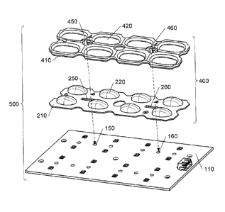
Referring now to Figure 2, an exploded view of a first
embodiment of a lens array assembly 400 is shown. The lens array
assembly 400 comprises the free form lens array 210 shown in Figure 1A
and a lens holder 410. The lens holder 410 comprises a frame having eight
apertures 420 shaped to receive a respective one of the secondary lens
CA 02913679 2015-11-30
,
,
14
elements 220 when assembled. The lens holder 410 has a first surface and
a second surface, the second surface being in contact with the first surface
of the free form lens array 210 when assembled, that is, the lens holder 410
is positioned over the free form lens array 210 and is not in contact with the
PCB 110. The second surface of the free form lens array 210 is in contact
with the PCB 110 when an LED module (as shown in Figure 6) is
assembled. It will be appreciated that, although not shown, the concave
portion 220B of each secondary lens element 220 is placed nearer to the
LED element which it is associated than the convex portion 220A.
The frame includes an aperture or hole 440 with which the
alignment pin 240 of the skirt portion 230 of the free form lens array 210
engages when assembled. This ensures correct alignment of the free form
lens array 210 with the lens holder 410 so that the secondary lens elements
220 are located within apertures 420 of the lens holder 410, with their
convex portions 220A above the frame, when the lens holder 410 is
assembled with the free form lens array 210.
Clips 450, 460 are provided as part of the lens holder 410 for
aligning with corresponding apertures or holes 250, 260 formed in the skirt
portion 230 of the free form lens array 210 as shown. As shown, the
apertures or holes 250, 260 may comprise elongate slots, but the apertures
or holes 250, 260 are not limited to such a configuration.
The clips 450, 460 extend through the apertures or holes 250,
260 when the frame 410 is assembled with the free form lens array 210 as
will be described in more detail below. The clips 450, 460 are moulded from
the same material as the frame and are integrally formed therewith.
When an LED module is assembled, as will be described in
more detail below, the clips 450, 460 extend through into corresponding
holes 150, 160 formed in the PCB 110.
CA 02913679 2015-11-30
Markings 470, 475 on the first surface of the frame 410 are
aligned with corresponding markings 270, 275 provided on the first surface
of the free form lens array 210, and in particular, on the skirt portion 230
thereof.
5 Figure 3
illustrates the lens array assembly 400 from
underneath, that is, from the second surface of the free form lens array 210.
As shown, the first surface of the free form lens array 210 is in contact with
the second surface of the lens holder array 410. Positioning pins 280, 290
are provided on the second surface of the free form lens array 210 which
10 engage with
corresponding apertures or holes 180, 190 provided in the PCB
110 (as described above with reference to Figure 1A).
The positioning pins 280, 290 are shaped to allow for thermal
expansion of an assembled LED module (not shown) without creating any
deformation in the free form lens array 210. In one embodiment as shown,
15 one pin 290 has a
circular cross-section and the other pin 280 has a
rhomboid (lozenge) cross-section. However, it will be appreciated that other
cross-sections are possible for the positioning pins 280, 290 as long as they
can accommodate dimensional changes due to thermal expansion.
The positioning pins 280, 290 provide correct referencing of the
free form lens array 210 with respect to the PCB 110 when inserted into
corresponding apertures 180, 190 in the PCB 110. This reference is
maintained between the free form lens array 210 and the PCB 110 with the
lens holder 410 being prevented from putting any mechanical constraint on
this positioning. In effect, the lens holder 410 is only used to maintain the
second surface of the free form lens array 210 in contact with the first
surface of the PCB 110.
As described above with reference to Figure 2, the lens holder
410 incorporates clips 450, 460 which provide a simple and rigid mounting of
CA 02913679 2015-11-30
16
the lens holder 410 to both the free form lens array 210 and the PCB 110.
The positioning of these clips 450, 460 and their flexibility is crucial to
maintain the lens holder 410 properly aligned with respect to the free form
lens array 210 and to the PCB 110 whilst adjusting for thermal expansion.
Figure 4 illustrates a perspective view of the lens holder 410
from underneath so that the location of the clips 450, 460 and the aperture
or hole 440 can clearly be seen. As described above, the clips 450, 460 are
flexible and are designed to have sufficient flexibility to adjust with
differences in thermal expansion between the material from which the PCB
110 is made and the material from which the lens holder 410 is made. Non-
limiting examples of materials from which the lens holder 410 may be made
include thermoplastic materials, for example, polycarbonate (PC),
polyphenylene sulphide (PPS), polybutylene terephthalate (PBT) and
polyamide (PA).
Figure 5 illustrates a top perspective view of the lens array
assembly 400. As shown, the markings 470, 475 and the aperture or hole
440 formed on or in the lens holder 410 are used to ensure that there is
correct orientation with the free form lens array 210. As described above,
markings 470, 475 are matched to corresponding markings 270, 275 on the
free form lens array 210 as shown in Figure 2. The aperture or hole 440 is
sized to accommodate the positioning pin 240 formed on the skirt portion
230 of the free form lens array 210, and is used as a "foolproof" mounting
mechanism.
The provision of the markings 270, 275 and pin 240 on the free
form lens array 210 and the markings 470, 475 and aperture or hole 440 on
the lens holder 410 ensures that lens holder 410 is correctly oriented with
the free form lens array 210 when being assembled. It will readily be
appreciated that other methods of ensuring that the free form lens array 210
CA 02913679 2015-11-30
,
,
17
is correctly oriented with respect to the lens holder 410 are possible, for
example, shaped protrusions may be formed on the lens holder which
engage corresponding depressions or apertures formed in the skirt portion
230 of the free form lens array 210.
Once the lens array assembly 400 has been assembled, the
clips 450, 460 integrally formed with the frame of the lens holder 410 extend
through correspond holes 250, 260 formed in the free form lens array 210
(shown in Figure 2), and, when mounted on the PCB 110, the clips 450, 460
extend through corresponding holes 150, 160 (shown in Figure 1A) to
complete a first embodiment of an LED module.
Figure 6 illustrates an exploded view of such an LED module
500 comprising the PCB 110 and the lens array assembly 400 which
comprises the free form lens array 210 and the lens holder 410 as described
above. As shown, the apertures or holes 250, 260 formed in the free form
lens array 210 may comprise elongate slots to allow for differences in
tolerances when the free form lens array 210 is moulded. These elongate
slots also provide compensation for any tolerances in the moulding of the
lens holder 410.
In addition, the LED module 500 may include a second lens
array assembly which is located alongside the lens array assembly 400 so
that both groups 120A, 120B of eight LED elements 120 (Figures 1A and
1B) on the PCB 110 are associated with secondary lens elements.
Alternatively, for PCB 110 having sixteen secondary lens
elements 120, the lens array assembly may comprise twice the size of the
lens array assembly 400 and is capable of being mounted over all of the
sixteen secondary lens elements 120. In this case, the lens holder may
comprise four clips instead of two to provide the desired mounting.
Moreover, the lens array assembly may comprise one free form lens array
CA 02913679 2015-11-30
s
18
having the requisite number of secondary lens elements and two lens
holders 410 may be employed to mount the single free form lens array.
Similarly, two free form lens arrays may be mounted using a single lens
holder.
5 It will readily
be understood that the LED module 500 can
easily be assembled in seconds without the need for any tools, the clips 450,
460 providing the engagement necessary to retain the components of the
LED module together.
An another embodiment of a lens holder 610 is shown in Figure
10 7. Lens holder
610 comprises a frame having eight apertures 620 shaped to
receive a respective one of the lens elements 220 of the free form lens array
210 shown in Figure 2 when assembled. The lens holder 610 has a first
surface and a second surface, the second surface being in contact with a
first surface of the free form lens array 210 when assembled in an identical
15 way to that of
the lens holder 410 described above with reference to Figures
2 to 6.
The frame includes an aperture or hole (not shown) with which
the alignment pin 240 of the skirt portion 230 of the free form lens array 210
engages when assembled. This ensures correct orientation of the free form
20 lens array 210
with the lens holder 610 so that the lens elements 220 are
located within apertures 620 of the lens holder 610 when the lens holder 610
is assembled with the free form lens array 210.
Clips 650, 660 are provided for engaging corresponding holes
250, 260 formed in the skirt portion 230 of the free form lens array 210 as
25 described above. The clips 650, 660 extend through the holes 650, 660
when the frame 610 is assembled with the free form lens array 610.
Markings 670, 675 on the first surface of the frame 610 are
aligned with corresponding markings 270, 275 provided on the first surface
CA 02913679 2015-11-30
19
of the free form lens array 210, and in particular, on the skirt portion 230
thereof. As described above with reference to Figures 2 and 3, secondary
lens elements 220 of the free form lens array 210 extend through apertures
620 in the frame so that the convex portion 220A of each secondary lens
element is above the frame of the lens holder 610.
The lens holder 610 further comprises eight louvre elements
695 which are used to prevent backlighting from a luminaire in which an LED
module including such a lens holder 610 is mounted. This is advantageous
to prevent unwanted illumination of house facades in a residential
environment.
The material of the lens holder 610 may be made from a light
absorptive or reflective material depending on the particular properties
required for the louvre elements 695. Alternatively, the lens holder 610 may
be made from the same materials as the lens holder 410 but with a suitable
coating to modify the light absorption or reflective properties thereof. In
one
embodiment, only one surface of a louvre element may be coated, that is,
the surface which is nearer to the secondary lens element 220.
As described above, the lens holder 610 may be of any
suitable size in accordance with the particular application of the LED module
(not shown) in which it is implemented.
As an alternative to the embodiment of the free form lens array
210 described above with reference to Figures 2 to 7, it is possible to mount
each secondary lens element separately on the PCB 110. In this case, each
lens element has its own positioning pins which engage with corresponding
positioning pins on the PCB 110. Whilst it is possible to mount the
secondary lens elements separately, this requires more work during
assembly to ensure that there is correct alignment with respect to associated
LED elements.
CA 02913679 2015-11-30
Referring now to Figure 8, an exploded view of another
embodiment of a lens array assembly 700 is shown. The lens array
assembly 700 comprises a collimator lens array 310 as described with
reference to Figure 1B and a lens holder 710. In this embodiment, the lens
5 holder 710 is positioned between the collimator lens array 310 and the
PCB
110 when an LED module (not shown) including such a collimator lens array
is assembled. The lens holder 710 comprises a frame having first and
second surfaces as described above with reference to lens holder 410
(Figures 2 to 6) and lens holder 610 (Figure 7).
10 On the first surface, eight recesses 720 are formed to receive
respective ones of the eight secondary lens elements 320 in the collimator
lens array 310. The recesses 720 are formed by shaped wall elements 725
extending from the frame and which are arranged, in pairs as shown, to
define the recesses. In the illustrated embodiment, each wall element 725
15 comprises two concave portions 725A, 725B, and, pairs of wall elements
725 are arranged to oppose one another with pairs of concave portions in
defining the recesses 720. Each concave portion 725A, 725B includes a clip
725C which cooperates with a clip of an opposed concave portion to engage
a secondary lens element 320 of the collimator lens array 310 as will be
20 .. described in more detail below.
Each recess 720 has a proximal end 720A and a distal end
720B, the proximal end 720A being located adjacent the frame and the distal
end 720B being spaced from the frame. In this particular embodiment, the
distance between the proximal end 720A and the distal end 7208 of a
.. recess is substantially the same as the height of each secondary lens
element 320 of the collimator lens array 310.
At the proximal end 720A of each recess 720, a circular
aperture 720C is provided in the frame so that the frame can be positioned
CA 02913679 2015-11-30
21
on the PCB 110 (Figure 1B) with the LED elements 120 mounted on the
PCB 110 being aligned with the circular apertures 720C.
As shown, each secondary lens element 320 of the collimator
lens array 310 is substantially conical with a proximal end 320A and a distal
end 320B, the distal end 3208 having a larger cross section than the
proximal end 320A. When the collimator lens array 310 is assembled within
the lens holder 710, the proximal end 320A and the distal end 320B of each
secondary lens element 320 is respectively aligned with the proximal end
720A and the distal end 7208 of each recess 720. The proximal end 320A
of each secondary lens element 320 is centred within the recess 720 with
respect to the circular aperture 7200 associated therewith, and, the distal
end 3200 is retained in position within the recess 720 by clips 7250 of the
opposing concave portions of the two wall elements 725 defining the recess
720. This will be described in more detail below with reference to Figures 9
and 10.
Figure 9 illustrates a perspective view of the lens array
assembly 700. As shown, each secondary lens element 320 is retained
within one recess 720 with the proximal portion 320A being located in the
circular aperture 7200 and the clips 7250 of the wall elements 725
surrounding a portion of the distal end 320B of the secondary lens element
320.
On the second surface of the lens holder 710, clips 750, 760
are provided which correspond to the clips 450, 460 of the lens holder 410
and the clips 650, 660 of the lens holder 610. In this embodiment, the clips
750, 760 do not extend through the collimator lens array 310 when the
collimator lens array 310 is assembled in the lens holder 710.
Alignment pins 780, 790 are provided for engaging respective
apertures or holes 180, 190 in the PCB 110. In this case, the alignment pins
CA 02913679 2015-11-30
22
780, 790 take the place of the positioning pins 280, 290 of the free form lens
array 210 (Figure 3) to ensure that there is alignment of the lens holder 710
with respect to the LED elements 120 on the PCB 110.
Correct positioning of the lens array assembly 700 with respect
to the LED elements 120 on the PCB 110 is guaranteed by the two
positioning pins 780, 790 located on the lens holder 710. As described
above with reference to Figure 3, the positioning pins may have the same or
different cross-sections to allow for changes due to thermal expansion of an
assembled LED module (not shown) without creating deformation in the
collimator lens array 310 or the lens holder 710. In the described
embodiment, positioning pin 780 has a rhomboid (lozenge) cross section,
and, positioning pin 790 has a circular cross-section. As described above,
any cross-section combination is possible as long as the positioning pin can
accommodate thermal expansion.
Although a wall element of a particular shaped is described
with reference to Figures 8 to 10 for the lens holder 710, it will readily be
appreciated that other differently shaped wall elements are also possible to
provide support for the collimator lens array 310. In addition, the collimator
lens array 310 may comprise secondary lens elements 320 which are
arranged in a different format within the array and connected together in a
different manner.
In accordance with the present invention, the free form lens
array and the collimator lens array are moulded in a single process so that
the secondary lens elements are connected to one another to provide easy
of handling during assembly of the lens arrays and then the final LED
module.
The embodiments described above with reference to Figures 2
to 7 (free form lens array 210) and Figures 8 to 10 (collimator lens array
310)
CA 02913679 2015-11-30
23
provide accurate positioning of flexible lenses over LED elements on a PCB
with the advantages of:
a) easy mounting in an industrial environment without the need for
tools;
b) no requirement for adhesives to fix the silicone lens arrays in
place over the LED array on the PCB;
c) no requirement for screws or other fixings which penetrate the
silicone lens arrays; and
d) the LED modules can operate at higher temperatures without
having optical distortions created in the secondary lens elements
due to thermal cycling and thermal degradation due to the higher
operational temperatures
In addition, by providing LED modules which have higher
operating temperatures due to the stability of optical grade silicone at such
temperatures, it is possible to operate the LED modules at these higher
temperatures in luminaires. This means that the luminaires can be operated
at higher currents to provide more luminous flux in the same luminaire
housing (as is the case for existing designs), or, for a given luminous flux,
the required heat dissipation capacity can be reduced with an accompanying
.. material cost saving (as would be the case for new designs).
Although the present invention has been described above with
respect to particular embodiments, it will readily be appreciated that other
embodiments are also possible.