Note: Descriptions are shown in the official language in which they were submitted.
CA 02914152 2015-11-30
DESCRIPTION
TITLE OF INVENTION
Surface-Coated Boron Nitride Sintered Body Tool
TECHNICAL FIELD
The present invention relates to a surface-coated boron nitride sintered body
tool, in which at least a cutting edge portion includes a cubic boron nitride
(hereinafter
also referred to as "cBN") sintered body and a coating film formed on the cBN
sintered
body.
BACKGROUND ART
There is a cutting tool formed of a cBN sintered body as a base member having
a surface on which a coating film made of ceramics or the like is formed
(which will be
hereinafter also referred to as a "coated cBN tool"). This cutting tool
exhibits
excellent wear resistance, and therefore, is used for cutting processing of
hardened steel.
As such a cutting tool, for example, W02010/150335 (PTD 1) and
W02012/005275 (PTD 2) each disclose a tool formed of a cBN sintered body
having a
surface coated with a coating film including a lower layer formed of multiple
layers
having specific ceramic compositions and an upper layer formed of a compound
layer.
Furthermore, a base member of a tool having a coating film is formed not only
of a cBN sintered body, for example, but also of cemented carbide and the like
(Japanese Patent Laying-Open No. 2008-188689 (PTD 3) and Japanese Patent
National
Publication No. 2008-534297 (PTD 4)).
CITATION LIST
PATENT DOCUMENT
PTD!: W02010/150335
PTD 2: W02012/005275
PTD 3: Japanese Patent Laying-Open No. 2008-188689
PTD 4: Japanese Patent National Publication No. 2008-534297
SUMMARY OF INVENTION
- 1 -
CA 02914152 2015-11-30
TECHNICAL PROBLEM
Recently, cutting processing is requiring extremely high precision. The
precision required in this case is that a work material after processing
exhibits excellent
surface roughness to such an extent that finish processing such as polishing
is not
required after the cutting processing. In other words, cutting processing is
required to
also provide finish processing, unlike the conventional technique. Therefore,
the
cutting distance, at which presctibed surface roughness can be maintained
(which will
be hereinafter also referred to as a "surface roughness life"), is recently
regarded as an
essential feature for determining the tool performance. The conventional
cutting tool,
however, has not yet come to have a surface roughness life that can
sufficiently satisfy
the current users. Therefore, the surface roughness life is often simply
regarded as a
tool life under the current circumstances, and it is strongly desired to
increase the
surface roughness life.
Various factors that exert influences upon the surface roughness of the work
material may be conceivable. Among others, the shape change of the insert
resulting
from wear is considered as a particularly influential factor. Accordingly,
improving
the wear resistance is considered as effective for increasing the surface
roughness life.
Until now, there have been developed cutting tools with wear resistance
improved by forming a coating film on the surface of the base member. For
example,
there is a cutting tool formed of a base member made of cemented carbide
having a
surface on which a coating film is formed. It is known that this cutting tool
exhibits
suitable wear resistance in steel processing.
In high precision processing of hardened steel higher in hardness than steel,
however, sufficient surface roughness life could not be obtained even if a
coating film
was formed, similarly to cemented carbide, on the surface of the base member
made of
a cBN sintered body. Thus, in the present circumstances, there has not yet
been
developed a cutting tool implementing a long life in high precision processing
of
hardened steel.
The present invention has been made in light of the above-described
- 2 -
= CA 02914152 2015-11-30
circumstances. An object of the present invention is to provide a coated cBN
tool
implementing high dimensional precision and having an excellent tool life in
processing of a hard material such as hardened steel.
SOLUTION TO PROBLEM
In order to solve the above-described problems, the present inventors have
processed hardened steel using a coated cBN tool covered with a coating film
having
various compositions and stacking structures, and they also carried out
detailed analysis
of the damaged state of the tool. The results showed that, in addition to
normal crater
wear and flank face wear, boundary wear also occurred in the front boundary
portion
corresponding to one end of the wear portion. Also, the present inventors
found that
this boundary wear exerted the most significant influence upon the surface
roughness
life.
As a result of repeated studies based on their findings described above, the
present inventors found that multiple layers having specific compositions were
effective for suppressing boundary wear. Then, they got an idea of combining a
layer
having boundary wear resistance and a layer having crater wear resistance so
that a
coating film having both of these resistance characteristics could be formed.
Thus,
upon having conducted earnest studies about means for implementing the above-
described idea, they found that not only both of these resistance
characteristics were
implemented, but also the surface roughness life was dramatically improved in
the case
where a special ceramic layer was arranged between the layer having boundary
wear
resistance and the layer having crater wear resistance. Consequently, the
present
inventors have completed the present invention.
Specifically, the surface-coated boron nitride sintered body tool of the
present
invention has configurations (1) to (9) described below.
(1) At least a cutting edge portion includes a cubic boron nitride sintered
body
and a coating film formed on a surface of the cubic boron nitride sintered
body.
(2) The cubic boron nitride sintered body includes 30 vol% or more and 80
vol% or less of cubic boron nitride particles, and further includes a binder
phase
- 3 -
= CA 02914152 2015-11-30
including: at least one compound selected from the group consisting of
nitride, carbide,
boride, oxide, and solid solutions thereof in group 4 elements, group 5
elements and
group 6 elements in a periodic table; an aluminum compound; and inevitable
impurities.
(3) The coating film includes an A layer, a B layer and a C layer.
(4) The A layer includes MLazai (M represents one or more of group 4 elements,
group 5 elements and group 6 elements in the periodic table, Al and Si; La
represents
one or more of B, C, N, and 0; and zal is 0.85 or more and 1.0 or less).
(5) The B layer is formed by alternately stacking one or more of each of two
or
more compound layers having different compositions, and the compound layers
each
have a thickness of 30 nm or more and 300 nm or less.
(6) A B1 compound layer that is one of the above-described compound layers
includes (Tii-xbi-ybiSixbiMlybi) (Ci-zbiNzbi) (M1 represents one or more of
group 4
elements except for Ti, group 5 elements and group 6 elements in the periodic
table,
and Al; xbl is 0.01 or more and 0.25 or less; ybl is 0 or more and 0.7 or
less; and zbl
is 0.4 or more and 1 or less).
(7) A B2 compound layer that is one of the above-described compound layers
and different from the B1 compound layer includes (Al1-xb2M2xb2) (C1-zb2Nzb2)
(M2
represents one or more of group 4 elements, group 5 elements and group 6
elements in
the periodic table, and Si; xb2 is 0.2 or more and 0.7 or less; and zb2 is 0.4
or more and
1 or less).
(8) The C layer is provided between the A layer and the B layer, and includes
McLczc (Mc represents one or more of group 4 elements, group 5 elements and
group 6
elements in the periodic table, Al and Si; Lc represents one or more of B, C,
N, and 0;
and zc is more than 0 and 0.85 or less).
(9) The A layer has a thickness of 0.21.1m or more and 10 jim or less, the B
layer
has a thickness of 0.05 p.m or more and 5 p.m or less, the C layer has a
thickness of
0.005 pm or more and 0.5 gm or less, and the coating layer has an entire
thickness of
0.3 pm or more and 15 gm or less.
ADVANTAGEOUS EFFECTS OF INVENTION
- 4 -
= CA 02914152 2015-11-30
,
The surface-coated boron nitride sintered body tool of the present invention
implements high dimensional precision and exhibits an excellent surface
roughness life
in processing of a hard material such as hardened steel.
BRIEF DESCRIPTION OF DRAWINGS
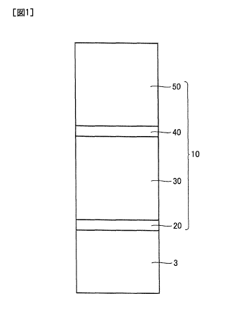
Fig. 1 is a cross-sectional view showing an example of the configuration of a
surface-coated boron nitride sintered body tool according to the present
embodiment.
Fig. 2 is a cross-sectional view showing an example of the configuration of a
main part of the surface-coated boron nitride sintered body tool according to
the present
embodiment.
DESCRIPTION OF EMBODIMENTS
The embodiments according to the present invention will be hereinafter
described in greater detail. While the following explanation will be made with
reference to the accompanying drawings, the same or corresponding components
are
designated by the same reference characters in the accompanying drawings of
the
present application.
<<Surface-Coated Boron Nitride Sintered Body Tool>>
In a coated cBN tool of the present embodiment, at least a cutting edge
portion
includes a cBN sintered body and a coating film formed on the surface of the
cBN
sintered body. As described later, the coating film is formed of an A layer
that is
excellent in crater wear resistance, a B layer that is excellent in boundary
wear
resistance, and a C layer firmly bonding the A layer and the B layer, thereby
achieving
an effect that high dimensional precision can be maintained for a long time
when
processing a sintered alloy, hard-to-cut cast iron, hardened steel and the
like, that is, the
surface roughness life is relatively long. Also, particularly for wet cutting
using a
cutting fluid, the coated cBN tool of the present embodiment can have a
remarkably
long surface roughness life as compared with the conventional cutting tool.
In wet cutting, a cutting fluid (which is also referred to as a coolant)
discontinuously comes into contact with an insert, so that rapid cooling and
rapid
heating of the insert are repeated. Also, in the case where the coating film
has a
- 5 -
= CA 02914152 2015-11-30
structure obtained by stacking a plurality of layers having different
characteristics such
as a chemical composition and thickness, there occurs a problem that
delamination is
more likely to occur due to difference in coefficient of thermal expansion and
the like.
In order to suppress this delamination, a method of providing a metal layer as
an
adhesion layer between the layers has been proposed. Such a metal layer
however
exhibited peeling resistance against mechanical deformation, but could not
achieve a
sufficient effect in a damage mode accompanied by boundary wear. It is
estimated
that this is because air is more likely to infiltrate into a boundary wear
portion, and the
insert is exposed to an elevated temperature, thereby causing the metal layer
to be
readily oxidized, so that the peeling resistance cannot be maintained. In
contrast,
according to the present embodiment, as a ceramics layer still keeping
metallic
characteristics as an adhesion layer (a C layer described later) is employed,
the
adhesion layer is provided with heat resistance and oxidation resistance so
that
adhesiveness can be maintained. Consequently, an excellent surface roughness
life
can be provided. Each of components forming the coated cBN tool of the present
embodiment will be hereinafter described.
<cBN Sintered Body>
A cBN sintered body of the present embodiment forms a base member for a
coated cBN tool in a cutting edge portion of the tool, includes 30 vol% or
more and 80
vol% or less of cBN particles, and further includes a binder phase as the
remainder.
In this case, the binder phase includes: at least one compound selected from
the
group consisting of nitride, carbide, boride, oxide, and solid solutions
thereof in group
4 elements, group 5 elements, and group 6 elements in the periodic table; an
aluminum
compound; and inevitable impurities. The binder phase binds the cBN particles
to
each other in the sintered body structure. As 30 vol% or more of cBN particles
are
contained, a decrease in wear resistance of the cBN sintered body as a base
member of
the tool can be prevented. Furthermore, as 80 vol% or less of cBN particles
are
contained, the cBN particles that are excellent in strength and toughness
serve as a
skeletal structure in the sintered body structure, so that the fracture
resistance of the
- 6 -
CA 02914152 2015-11-30
cBN sintered body can be ensured.
In the present specification, the volume content of the cBN particles is to be
measured by the method described below. Specifically, a cBN sintered body is
mirror-polished, and the backscattered electron image of the cBN sintered body
structure in an arbitrary region is observed by using an electron microscope
at 2000
times magnification. In this case, the cBN particles are observed as a black
area while
the binder phase is observed as a gray area or a white area. In an observation
view
image, the cBN particle region and the binder phase region are binarized by
image
processing to measure the occupancy area of the cBN particle region. Then, the
occupancy area is substituted into the following equation, thereby calculating
the
volume content of the cBN particles.
(Volume content of cBN particles) = (occupancy area of cBN particles) (area
of cBN sintered body structure in view image) x 100.
It is preferable that the volume content of the cBN particles is 50 vol% or
more
and 65 vol% or less. As the volume content of the cBN particles is 50 vol% or
more,
the coated cBN tool tends to exhibit an excellent balance between the wear
resistance
and the fracture resistance. Furthermore, as the volume content of the cBN
particles is
65 vol% or less, the binder phase is to be distributed appropriately, so that
the bonding
strength of the cBN particles by the binder phase tends to increase.
Furthermore, it is preferable that the cBN particles are shaped to protrude
more
to the coating film than to the binder phase at the interface between the cBN
sintered
body and the coating film. Thereby, the adhesiveness between the cBN sintered
body
and the coating film can be improved. Furthermore, it is preferable that the
difference
in level between the cBN particles and the binder phase is 0.05 gm or more and
1.0 gm
or less. As the difference in level is 0.05 gm or more, an anchor effect can
be
achieved. Furthermore, as the difference in level is 1.0 gm or less, the cBN
particles
can be effectively prevented from falling off from the sintered body. In this
case, the
difference in level is more preferably 0.1 gm or more and 0.5 gm or less. If
the
difference in level falls within this range, the anchor effect and the fall-
off preventing
- 7 -
CA 02914152 2015-11-30
effect described above can be further improved. In the present specification,
the
difference in level is to be measured by the same method as the method of
measuring
the thickness and the like of the entire coating film, which will be described
later.
Furthermore, it is preferable that the cBN particles in the cBN sintered body
are
increased in volume content from the interface between the cBN sintered body
and the
coating film toward the inside of the cBN sintered body. By such a
configuration, the
volume content of the binder phase is higher at the interface between the cBN
sintered
body and the coating film than that of the cBN particles, so that the
adhesiveness
between the cBN sintered body and the coating film can be improved. In
contrast, on
the inside of the cBN sintered body, the volume content of the cBN particles
is higher
than that of the binder phase, so that the fracture resistance of the cBN
sintered body
can be improved. For example, the volume content of the cBN particles can be
set at
40 vol% in an area close to the interface with the coating film (that is, in
the region
located at a distance of 0 gm or more and 20 gm or less from the interface
between the
cBN sintered body and the coating film toward the cBN sintered body-side), and
can be
set at 60 vol% near the center of the cBN sintered body in the thickness
direction (that
is, in the region located at a distance of more than 20 gm and 100 gm or less
from the
interface between the cBN sintered body and the coating film toward the inside
of the
cBN sintered body).
Furthermore, it is preferable that the cBN particles are increased in particle
size
from the interface between the cBN sintered body and the coating film toward
the
inside of the cBN sintered body. In such a configuration, the particle size of
each
cBN particle is relatively small at the interface between the cBN sintered
body and the
coating film, so that the adhesiveness between the cBN sintered body and the
coating
film can be improved. On the other hand, since the particle size of each cBN
particle
is relatively large on the inside of the cBN sintered body, the toughness can
be
improved. For example, the particle size of each cBN particle can be set at
0.1 gm or
more and 1 gm or less in the region located at a distance of 0 gm or more and
20 gm or
less from the interface between the cBN sintered body and the coating film
toward the
- 8 -
CA 02914152 2015-11-30
inside of the cBN sintered body, and can be set at 2 pm or more and 10 pm or
less in
the region located at a distance of more than 20 pm and 300 pm or less from
the
interface between the cBN sintered body and the coating film toward the inside
of the
cBN sintered body.
In the present specification, the particle size of each cBN particle is to be
measured by the following method. Specifically, the diameter of the circle
circumscribing the cBN particle (that is, a circumscribed circle equivalent
diameter) is
measured in the backscattered electron image of the cBN sintered body
structure
obtained when the volume content of the cBN particles is calculated. Then,
this
diameter is defined as a particle size of the cBN particle.
Furthermore, in the present embodiment, the cBN sintered body only has to be
provided in the cutting edge portion of the coated cBN tool. In other words,
the base
member of the coated cBN tool may include a cutting edge portion formed of a
cBN
sintered body, and a base member main body made of a material different from
that of
the cBN sintered body (for example, cemented carbide). In this case, it is
preferable
that the cutting edge portion formed of a cBN sintered body is bonded to the
base
member main body with a braze material and the like. The braze material may be
selected as appropriate in consideration of the bonding strength and the
melting point.
In addition, the cBN sintered body may form the entire base member of the
coated cBN
tool.
<Coating Film>
The coating film of the present embodiment includes an A layer, a B layer and
a
C layer. In the present embodiment, the coating film can include any layers
other than
these A, B and C layers as long as it includes these A, B and C layers. Even
if the
coating film includes other layers, the effect of the present invention can be
achieved.
In this case, other layers may for example be a D layer as the lowermost layer
described
later, and the like. It is to be noted that other layers are not limited to
those described
above and do not deviate from the scope of the present invention even if
layers other
than those described above are included.
- 9 -
CA 02914152 2015-11-30
In the present embodiment, the thickness of the entire coating film is 0.3 gm
or
more and 15 gm or less. As the thickness of the coating film is 0.3 gm or
more, it
becomes possible to prevent a decrease in wear resistance of the coated cBN
tool
resulting from a thin coating film. Furthermore, as the thickness of the
entire coating
film is 15 gm or less, the chipping resistance of the coating film in the
early stage of
cutting can be improved. The thickness of the entire coating film is more
preferably
1.5 gm or more and 15 gm or less.
In the present specification, each thickness of the coating film and each
layer
described later, and the number of stacked layers were measured by observing a
cross
section, which was obtained by cutting the coated cBN tool, with a scanning
electron
microscope (SEM) or a transmission electron microscope (TEM). Furthermore, the
composition of each of layers forming a coating film was measured by an energy
dispersive X-ray spectroscopy (EDX) attached to the SEM or the TEM. In this
case,
the sample for cross-section observation can be produced, for example, using a
focused
ion beam system (FIB), a cross section polisher (CP), and the like.
Also, in the present embodiment, the coating film needs to be provided only in
the cutting edge portion of the coated cBN tool, and does not need to be
provided in a
part of the portion different from the cutting edge portion or may cover the
entire
surface of the base member of the coated cBN tool. Also, the stacking
configuration
in a part of the coating film may be partially different in a portion
different from the
cutting edge.
<A Layer>
In the present embodiment, the A layer includes MLazai (M represents one or
more of group 4 elements, group 5 elements and group 6 elements in the
periodic table,
Al and Si; La represents one or more of B, C, N, and 0; and za 1 is 0.85 or
more and 1.0
or less). Thereby, the A layer smoothly wears out during cutting processing.
In
other words, the A layer can wear out without undergoing peeling, cracking,
chipping,
or the like. Therefore, the crater wear resistance, the flank face wear
resistance or the
like of the coated cBN tool can be improved.
- 10-
CA 02914152 2015-11-30
It is more preferable that the above-described A layer includes (Tii-xaMaxa)
(C1 -
za2Nza2) (Ma represents one or more of group 4 elements except for Ti, group 5
elements and group 6 elements in the periodic table, Al and Si; xa is 0 or
more and 0.7
or less; and za2 is 0 or more and 1 or less). In this way, the A layer
containing Ti can
further effectively prevent peeling, cracking, chipping or the like in the A
layer when
wear occurs. In this case, it is more preferable that the above-mentioned xa
is 0 or
more and 0.3 or less. As xa falls within this range, the above-described
effect can be
further more improved. In the case where the A layer includes (Ti 1-xa(1 )-
xa(2)Ma( 1 )xa(1)
Ma(2)xa(2)) (C1-za2Nza2), the sum of xa(1) and xa(2) is preferably 0 or more
and 0.7 or
less, and more preferably 0 or more and 0.3 or less. This also similarly
applies to the
B layer, the C layer and the D layer which will be described later.
According to the present embodiment, in the A layer, it is preferable that the
composition (za2) of N described above changes in a step-like manner or in a
slope-like
manner from the cBN sintered body-side toward the surface-side of the A layer.
For
example, in the case where the composition of N is relatively large on the cBN
sintered
body-side of the A layer, the fracture resistance and the peeling resistance
tends to
increase. Furthermore, for example, in the case where the composition of N is
relatively small on the surface-side of the A layer, peeling, cracking,
chipping or the
like of the A layer during wearing can be prevented. In this case, the
expression that
"the composition of N changes in a step-like manner from the cBN sintered body-
side
toward the surface-side of the A layer" means that the composition of N
discontinuously decreases or increases from the cBN sintered body-side toward
the
surface-side of the A layer, for example, which is a configuration in which
the
composition of N is obtained by stacking two or more different layers.
Furthermore,
the expression that "the composition of N changes in a slope-like manner from
the cBN
sintered body-side toward the surface-side of the A layer" means that the
composition
of N continuously decreases or increases from the cBN sintered body-side
toward the
surface-side of the A layer, for example, which is a configuration obtained by
continuously changing the flow rate ratio between raw material gas of N and
raw
-11-
CA 02914152 2015-11-30
material gas of C when the A layer is formed by the arc ion plating method.
Furthermore, it is preferable that the A layer is provided on its surface-side
with
a region where the composition of C is larger than that on its cBN sintered
body-side.
Thereby, the fracture resistance and the peeling resistance increase on the
cBN sintered
body-side of the A layer while peeling, cracking, chipping or the like of the
A layer
during wearing can be effectively prevented on the surface-side of the A
layer. In this
case, the cBN sintered body-side of the A layer means a region located at a
distance of
0 gm or more and 0.1 lam or less from the surface of the A layer located
closest to the
cBN sintered body toward the inside of the A layer. Furthermore, the surface-
side of
the A layer shows a portion of the A layer that is different from its cBN
sintered body-
side.
The thickness of the A layer in the present embodiment is 0.2 gm or more and
10 gm or less. As the thickness of the A layer is 0.2 gm or more, the crater
wear
resistance, the flank face wear resistance or the like of the coated cBN tool
tends to
increase. If the thickness of the A layer exceeds 10 gm, it may be difficult
to improve
the crater wear resistance, the flank face wear resistance or the like.
Therefore, the
thickness of the A layer needs to be 10 gm or less. The thickness of the A
layer is
more preferably 1 gm or more and 3 gm or less.
Furthermore, in the present embodiment, it is preferable that the A layer is
provided closer to the surface-side of the coated cBN tool than the B layer
described
later. Thereby, the A layer smoothly wears out so that occurrence of cracking
can be
suppressed. Furthermore, even if cracking occurs, the B layer can prevent this
cracking from spreading to the base member-side.
<13 Layer>
In the present embodiment, the B layer is formed by alternately stacking one
or
more of each of two or more compound layers having different compositions. The
following shows a configuration obtained by alternately stacking one or more
of each
of a B1 compound layer and a B2 compound layer. As long as the B layer in the
present embodiment includes a B1 compound layer and a B2 compound layer, the
- 12 -
CA 02914152 2015-11-30
effects of the present invention can be achieved even if this B layer includes
layers
other than the B1 compound layer and the B2 compound layer. In addition, the
thickness of the B layer is 0.05 gm or more and 5 gm or less.
<B1 Compound Layer>
The B1 compound layer forming a B layer includes (Tii-xbi-ybi SixbiMlybi) (CI-
zbINzbi) (Ml represents one or more of group 4 elements except for Ti, group 5
elements and group 6 elements in the periodic table, and Al; xbl is 0.01 or
more and
0.25 or less; ybl is 0 or more and 0.7 or less; and zb 1 is 0.4 or more and 1
or less). In
this case, the thickness of the B1 compound layer is 30 nm or more and 300 nm
or less,
more preferably 30 nm or more and 200 nm or less, and particularly preferably
30 nm
or more and 100 nm or less.
<B2 Compound Layer>
The B2 compound layer forming a B layer together with the B1 compound layer
includes (Ali-xb2M2xb2) (C1-zb2Nzb2) (M2 represents one or more of group 4
elements,
group 5 elements and group 6 elements in the periodic table, and Si; xb2 is
0.2 or more
and 0.7 or less; and zb2 is 0.4 or more and 1 or less). In this case, it is
preferable that
M2 represents at least one of Ti and Cr. As the B2 compound layer includes Al
and at
least one of Ti and Cr, the B2 compound layer can be provided with a function
as a
layer with high toughness, which has both of wear resistance and heat
resistance.
Furthermore, a composition xb2 of M2 is preferably 0.25 or more and 0.5 or
less, and more preferably 0.25 or more and 0.4 or less. Furthermore, the
thickness of
the B2 compound layer is 30 nm or more and 300 nm or less, more preferably 50
nm or
more and 300 nm or less, and particularly preferably 100 nm or more and 200 nm
or
less.
In addition, the lowermost layer of the B layer may be a B1 compound layer or
a B2 compound layer. Furthermore, the uppermost layer of the B layer may be a
B1
compound layer or a B2 compound layer.
In the present embodiment, it is preferable that the ratio between an average
thickness tl of the B1 compound layers and an average thickness t2 of the B2
- 13 -
CA 02914152 2015-11-30
compound layers is defined as t2/t1, which satisfies the relation of 0.5
<t2/t1 10Ø
In the present specification, average thickness ti of the B1 compound layers
is
calculated using the following calculation formula (the same applies to
average
thickness t2 of the B2 compound layers).
(Average thickness ti of B1 compound layers) = (total thickness of Bl
compound layers) (the number of B1 compound layers).
Furthermore, in the case where it is difficult to measure the thickness of the
B1
compound layer, average thickness ti of the BI compound layers can be
calculated
using the following calculation formula (the same also applies to average
thickness t2
of the B2 compound layers).
(Average thickness ti of B1 compound layers) = (thickness of B layer formed
by stacking only B1 compound layers) (the number of stacked B1 compound
layers).
As the above-mentioned t2/t1 satisfies the relation of 0.5 <t2/t1 10.0, the
boundary wear resistance and the like in the coated cBN tool are remarkably
improved.
Therefore, even under the severe operating conditions that impacts and
vibrations are
repeatedly applied, for example, as in the case of interrupted cutting, a
sufficient
surface roughness life can be provided. In this case, t2/t1 more preferably
satisfies the
relation of 1.6 <t2/t1 5.0, and further preferably satisfies the relation of
3.0 <t2/t1
4Ø
<C Layer>
The coating film of the present embodiment includes a C layer provided
between the A layer and the B layer. This C layer includes McLczc (Mc
represents
one or more of group 4 elements, group 5 elements and group 6 elements in the
periodic table, Al and Si; Lc represents one or more of B, C, N, and 0; and zc
is more
than 0 and 0.85 or less). The compound having such a composition can have both
of:
metallic characteristics of bonding the A layer and the B layer; and ceramic
characteristics that are excellent in heat resistance and oxidation
resistance. Therefore,
the coated cBN tool of the present embodiment exhibits an excellent surface
roughness
life also in a damage mode accompanied by boundary wear.
- 14 -
CA 02914152 2015-11-30
Furthermore, the thickness of the C layer is 0.005 gm or more and 0.5 gm or
less. As the thickness of the C layer is 0.005 or more, the adhesiveness
between the A
layer and the B layer can be improved. Furthermore, as the thickness of the C
layer is
0.5 gm or less, the thickness of the coating film can be prevented from being
excessively increased by the C layer. In this case, the thickness of the C
layer is
preferably 0.01 gm or more and 0.2 gm or less.
In the above-described McLczc, it is preferable that a composition zc of Lc is
more than 0 and less than 0.7. As zc is more than 0, the heat resistance and
the
chemical wear resistance of the C layer can be improved, and cracking
occurring in the
A layer can be blocked from spreading toward the base member-side. In
addition, zc
is more preferably 0.2 or more and 0.5 or less.
Furthermore, it is preferable that the C layer includes at least one or more
of
elements forming the A layer and the B layer. As the C layer includes the same
element as that included in the A layer in this way, the adhesiveness between
the C
layer and the A layer can be improved. Furthermore, as the C layer includes
the same
element as that included in the B layer, the adhesiveness between the C layer
and the B
layer can be improved. Also, it is suitable that the C layer includes at least
one or
more of elements forming a portion in each of the A layer and the B layer that
is
located on the C layer-side because the adhesiveness tends to be further
improved.
<D Layer>
It is preferable that the coating film of the present embodiment further
includes
a D layer provided between the base member and the B layer. It is preferable
that this
D layer includes MdLdni (Md represents one or more of group 4 elements, group
5
elements and group 6 elements in the periodic table, Al and Si; Ld represents
one or
more of B, C, N, and 0; and zd is 0.85 or more and 1.0 or less). Such a D
layer is
excellent in adhesiveness with the cBN sintered body. Therefore, the coating
film
including the D layer can improve the adhesiveness between the coating film
and the
cBN sintered body. In addition, Ld is more preferably N.
In this case, it is more preferable that the D layer includes (Al i_xaMd2xci)
Ldzd
- 15-
CA 02914152 2015-11-30
(Md2 represents one or more of group 4 elements, group 5 elements and group 6
elements in the periodic table, and Si; and xd is 0.25 or more and 0.45 or
less). In this
way, it is suitable that the D layer contains Al since the adhesiveness
between the
coating film and the cBN sintered body tends to be further increased. It is
considered
that this is because the compound containing Al as in the above-described
general
formula is strongly bonded not only to the cBN particles but also to the
binder phase in
the cBN sintered body. In addition, Md2 is more preferably at least one or
more of Ti,
Cr, and V.
Furthermore, it is preferable that the thickness of the D layer is 0.05 gm or
more
and 1 gm or less. As the thickness of the D layer is 0.05 gm or more, the
adhesiveness between the coating film and the cBN sintered body can be
improved.
Also, as the thickness of the D layer is 1 gm or less, the thickness of the
coating film
can be prevented from being excessively increased by the D layer. In this
case, the
thickness of the D layer is more preferably 0.1 gm or more and 0.5 gm or less.
<<Method of Manufacturing Coated cBN Tool>>
A method of manufacturing a coated cBN tool according to the present
embodiment includes for example the steps of: preparing a base member in which
at
least a cutting edge portion includes a cBN sintered body; and forming a
coating film
on the cBN sintered body.
<Step of Preparing Base Member>
The base member of the present embodiment can be manufactured by bonding a
base member main body and a base member formed of a cBN sintered body. The
base member main body can be made using a material, for example, cemented
carbide.
Such a base member main body can be manufactured, for example, by the
conventionally known sintering method and molding method. Furthermore, the
base
member formed of a cBN sintered body can be manufactured, for example, by
sintering
a mixture made of cBN particles and raw material powder of a binder phase
under
high-temperature and high-pressure conditions. Then, the base member formed of
a
cBN sintered body is bonded with the conventionally known braze material to an
- 16 -
= CA 02914152 2015-11-30
appropriate portion of the base member main body, which is then subjected to
grinding
processing and formed into a prescribed shape, with the result that the base
member can
be manufactured. In addition, it is a matter of course that the entire base
member is
formed of a cBN sintered body.
<Step of Forming Coating Film>
A coating film is formed on the base member obtained as described above, so
that a coated cBN tool can be manufactured. In this case, it is preferable
that the step
of forming an coating film includes the step of forming a coating film by the
arc ion
plating method (the ion plating method for evaporating a solid material by
utilizing
vacuum arc discharge) or by the sputtering method. According to the arc ion
plating
method, a coating film can be formed using: a metal evaporation source
containing
metal species for forming a coating film; and reaction gas such as CH4, N2 or
02. In
addition, the conditions for forming a coating film can be conventionally
known
conditions. According to the sputtering method, a coating film can be formed
using: a
metal evaporation source containing metal species for forming a coating film;
reaction
gas such as CH4, N2, or 02; and sputtering gas such as Ar, Kr, and Xe. Also in
this
case, the conditions for forming a coating film can be conventionally known
conditions.
Examples
Although the present invention will be hereinafter described in greater detail
with reference to Examples, the present invention is not limited thereto.
<<Manufacture of Coated cBN Tool>>
Fig. 1 is a cross-sectional view showing an example of the configuration of a
coated cBN tool in Example. Fig. 2 is a cross-sectional view showing an
example of
the configuration of a main part of the coated cBN tool in Example.
<Manufacture of cBN Sintered Body>
As described below, cBN sintered bodies A to I each having a composition
shown in Table I were manufactured. Each compound shown in the column of "X-
ray Detecting Compound" in Table 1 is a compound detected when qualitatively
analyzing the cross section or the surface of the cBN sintered body by an X-
ray
- 17 -
= CA 02914152 2015-11-30
=
diffraction (XRD) apparatus.
(Manufacture of cBN Sintered Body A)
First, a mixture was obtained by mixing TiN powder having an average particle
size of 1 p.m and Ti powder having an average particle size of 3 pm in an
atomic ratio
of Ti:N=1:0.6. This mixture was heat-treated for 30 minutes at 1200 C in a
vacuum
and then ground. Thereby, intermetallic compound powder made of TiNo 6 was
obtained.
Then, a mixture was obtained by mixing intermetallic compound powder made
of TiNo 6 and Al powder having an average particle size of 4 pm in a mass
ratio of
TiN06:Al = 90:10. This mixture was heat-treated for 30 minutes at 1000 C in a
vacuum. The compound obtained by the heat treatment was uniformly ground by
the
ball-milling method using ball media made of cemented carbide and having a
diameter
of 6 mm. Thereby, raw material powder of the binder phase was obtained.
Then, cBN particles having an average particle size of 1.5 pm and raw material
powder of the binder phase were blended so as to achieve 30 vol% of the
content of the
cBN particles in the cBN sintered body, and then, uniformly mixed by the ball
mill
mixing method using ball media made of boron nitride and having a diameter of
3 mm,
thereby obtaining powdery mixture. Then, this mixture was stacked on a support
substrate made of cemented carbide, and then introduced into a capsule made of
Mo,
which was then sintered for 30 minutes at pressure of 5.5 GPa and at a
temperature of
1300 C using an ultra-high pressure apparatus. Thereby, a cBN sintered body A
was
obtained.
(Manufacture of cBN Sintered Bodies B to G)
As shown in Table 1, cBN sintered bodies B to G were obtained in the same
manner as with cBN sintered body A, except that cBN particles having different
volume contents and different average particle sizes were used.
(Manufacture of cBN Sintered Body H)
First, a mixture was obtained by mixing TiCN powder having an average
particle size of 1 pm and Ti powder having an average particle size of 3 pm in
an
- 18-
= CA 02914152 2015-11-30
=
atomic ratio of Ti:C:N = 1:0.3:0.3. Then, this mixture was heat-treated for 30
minutes
at 1200 C in a vacuum and then ground. Thereby, intermetallic compound powder
made of TiCo 3NO 3 was obtained.
Then, a mixture was obtained by mixing intermetallic compound powder made
of TiCo 3NO 3 and Al powder having an average particle size of 4 gm in a mass
ratio of
TiCo3NO3:Al = 90:10. This mixture was heat-treated for 30 minutes at 1000 C
in a
vacuum. The compound obtained by the heat treatment was uniformly ground by
the
ball-milling method using ball media made of cemented carbide and having a
diameter
of 6 mm. Thereby, raw material powder of the binder phase was obtained. Then,
the
raw material powder of the binder phase was used to obtain a cBN sintered body
H in
the same manner as with cBN sintered body A, except that cBN particles having
different volume contents and different average particle sizes were used, as
shown in
Table 1.
(Manufacture of cBN Sintered Body I)
First, a mixture was obtained by mixing TiC powder having an average particle
size of 1 gm and Ti powder having an average particle size of 3 gm in an
atomic ratio
of Ti:C = 1:0.6. This mixture was heat-treated for 30 minutes at 1200 C in a
vacuum
and then ground. Thereby, intermetallic compound powder made of TiCo 6 was
obtained.
Then, a mixture was obtained by mixing intermetallic compound powder made
of TiCo 6 and Al powder having an average particle size of 4 gm in a mass
ratio of
TiC06:Al = 90:10. This mixture was heat-treated for 30 minutes at 1000 C in a
vacuum. The compound obtained by the heat treatment was uniformly ground by
the
ball-milling method using ball media made of cemented carbide and having a
diameter
of 6 mm. Thereby, raw material powder of the binder phase was obtained. Then,
the
raw material powder of the binder phase was used to obtain a cBN sintered body
I in
the same manner as with cBN sintered body A, except that cBN particles having
different volume contents and different average particle sizes were used, as
shown in
Table 1.
- 19 -
CA 02914152 2015-11-30
[Table 1]
cBN Particles
Raw Material
cBN Sintered Volume Average X-ray Detecting
Powder
Body Content Particle Size Compound
of Binder Phase
(Vol%) (pm)
A 30 1.5 TiNo 6, Al cBN, TiN, TiB2(AIB2)
80 1.5 TiN0.6, Al cBN, TiN, TiB2(AIB2)
50 1.5 TiNo 6, Al cBN, TiN, TiB2(AIB2)
58 1.5 TiNo 6, Al cBN, TiN, TiB2(AIB2)
65 1.5 TiN0.6, Al cBN, TiN, TiB2(AIB2)
58 0.5 TiNo 6, Al cBN, TiN, TiB2(AIB2)
58 3 TiN06, Al cBN, TiN, T1B2(AIB2)
58 1.5 TiCO3N0 3, Al cBN, TiCN,
TiB2(AI82)
58 1.5 TiCo 6, Al cBN, TiC, TiB2(AIB2)
<Manufacture of Sample 1>
A coated cBN tool according to Sample 1 was manufactured as described below.
<Formation of Base Member>
A base member main body having a shape of DNGA150408 of the ISO
standard and made of a cemented carbide material (equivalent to K10) was
prepared.
The above-described cBN sintered body A (shape: a 2-mm-thick triangular prism
having isosceles triangles as bases whose vertex angle was 55 and sides
sandwiching
the vertex angle were each 2 mm) was bonded to an insert (corner portion) of
this base
member main body. A braze material made of Ti-Zr-Cu was used for bonding.
Then, the outer circumferential surface, the upper surface and the lower
surface of the
bonded body were ground to form a negative land shape (a negative land width
of 150
gm and a negative land angle of 25 ) at the insert. In this way, a base member
3
having a cutting edge portion formed of cBN sintered body A (see Fig. 1) was
obtained.
<Formation of Coating Film>
(Film Forming Apparatus)
- 20 -
CA 02914152 2015-11-30
A film forming apparatus used for forming a coating film will be hereinafter
described in the subsequent steps. A vacuum pump is connected to the film
forming
apparatus, within which a vacuum chamber that can be evacuated is provided. A
rotary table is placed inside the vacuum chamber. This rotary table is
configured such
that the base member can be placed thereon through a jig. The base member
placed
within the vacuum chamber can be heated by a heater placed inside the vacuum
chamber. Also, a gas pipe for introducing gas for etching and film forming is
connected to the vacuum chamber through a mass flow controller (MFC) for flow
rate
control. Furthermore, a tungsten filament for generating Ar ions for etching,
or an arc
evaporation source or a sputtering source for film formation to which a
necessary
power supply is connected is disposed within the vacuum chamber. Then,
evaporation source raw material (target) required for film formation is placed
in the arc
evaporation source or the sputtering source.
(Etching of Base Member)
Base member 3 obtained as described above was placed within the vacuum
chamber of the film forming apparatus, and the chamber was evacuated. Then,
base
member 3 was heated to 550 C while rotating the rotary table at 3 rpm. Then,
Ar gas
was introduced into the vacuum chamber, a tungsten filament was discharged to
generate Ar ions, a bias voltage was applied to base member 3, and base member
3 was
etched by Ar ions. The etching conditions in this case are as described below.
Pressure of Ar gas: 1 Pa
Substrate bias voltage: ¨500V.
(Formation of D Layer)
Then, a D layer 20 was formed on base member 3 within the above-described
film forming apparatus. Specifically, the D layer was formed while adjusting
the
vapor deposition time so as to achieve a thickness of 0.1 pm under the
conditions
described below.
Target: Al (50 atom%), Ti (50 atom%)
Introduced gas: N2
- 21 -
CA 02914152 2015-11-30
Film forming pressure: 4 Pa
Arc discharge current: 150A
Substrate bias voltage: ¨35V
Table rotation speed: 3 rpm.
(Formation of B Layer)
Subsequently to D layer 20, a B layer 30 was formed on D layer 20 within the
film forming apparatus described above. Specifically, B1 compound layer 31 and
B2
compound layer 32 were alternately formed each for 10 times repeatedly under
the
conditions described below, so that a B layer 30 formed of 20 layers in total
and having
a total thickness of 1.4 pm was formed (see Fig. 2). When forming the B layer,
the
vapor deposition time was adjusted to achieve B1 compound layer 31 having a
thickness of 40 nm and B2 compound layer 32 having a thickness of 100 nm. In
Sample 1, the lowermost layer of the B layer is B1 compound layer 31 while the
uppermost layer thereof is B2 compound layer 32.
(Formation of B1 Compound Layer)
The B1 compound layer was formed under the conditions described below.
Target: Ti (92 atom%), Si (8 atom%)
Introduced gas: N2
Film forming pressure: 4 Pa
Arc discharge current: 150A
Substrate bias voltage: ¨40V.
Table rotation speed: 3 rpm.
(Formation of B2 Compound Layer)
The B2 compound layer was formed under the conditions described below.
Target: Al (50 atom%), Ti (50 atom%)
Introduced gas: N2
Film forming pressure: 4 Pa
Arc discharge current: 150A
Substrate bias voltage: ¨40V.
- 22 -
CA 02914152 2015-11-30
Table rotation speed: 3 rpm.
(Formation of C Layer)
Then, C layer 40 was formed on B layer 30 under the conditions described
below. The thickness of C layer 40 was set at 0.01 p.m by adjusting the vapor
deposition time.
Target: Ti
Introduced gas: N2, Ar (flow rate ratio between N2 and Ar set at 1:1)
Film forming pressure: 0.5 Pa
Arc discharge current: 160A
Substrate bias voltage: ¨200V
Table rotation speed: 3 rpm.
(Formation of A Layer)
After forming C layer 40, an A layer 50 was formed on C layer 40 under the
conditions described below. In this case, the flow rate of the introduced gas
(N2 and
CH4) was adjusted so as to be set at C:N = 1:4 in A layer 50. The thickness of
the A
layer 50 was set at 0.1 p.m by adjusting the vapor deposition time.
Target: Ti
Introduced gas: N2, CH4
Film forming pressure: 2 Pa
Arc discharge current: 180A
Substrate bias voltage: ¨350V
Table rotation speed: 3 rpm.
As described above, a coated cBN tool according to Sample 1 including coating
film 10 obtained by stacking D layer 20, B layer 30, C layer 40, and A layer
50 in this
order on base member 3 was obtained.
<Manufacture of Samples 2 to 7>
Coated cBN tools according to Samples 2 to 7 were obtained in the same
manner as with Sample 1 except that, when forming the A layer, the thickness
of the A
layer was changed as shown in Table 2 by adjusting the vapor deposition time.
- 23 -
CA 02914152 2015-11-30
<Manufacture of Samples 8 to 63>
As shown in Tables 2 and 3, coated cBN tools according to Samples 8 to 63
were manufactured using cBN sintered bodies A to I. In Tables 2 and 3, each
Sample
marked with a symbol "*" in the left-side column represents a coated cBN tool
according to each Example. For each of these Samples, a coating film was
formed
while appropriately making an adjustment within a range of the film forming
conditions described below so as to achieve each layer shown in Tables 2 and
3.
(Film Forming Conditions)
Target: metallic element shown in the composition column of each layer in
Tables 2 and 3
Introduced gas: appropriately select one or more from Ar, N2, and CH4
Film forming pressure: 0.1 Pa to 7 Pa
Arc discharge current: 60A to 300A
Substrate bias voltage: ¨700V to ¨25V
Table rotation speed: 2 rpm to 10 rpm.
- 24 -
. . CA 02914152 2015-11-30
[Table 2]
A La er C Lsyer BLayer D La
;--
cast 111:k-ness
coated cf Entire
Slated MLazai MoLom
MdLclzd
cBN Tool Coaling
Body
Ttide
Composition ligi COMpOSOn ness
COMPOSibOn. Ell Orn)
=MIME al
1.6
U 2 0.3
1.8
11 3 0.8
23
U 4 A TICo2Na8 1.5 Ti Nos 0.01 AlosTiosN
0.1 3.0
El 5 2
as
U 6 7
as
M 7 12
13.5
1111 8 Ti
II 9 TIN0.2
Ell 10 6 TCN*1 1.5 TjNas 0.05
Alo.7Cr03N 02 2.8
1111 1 1 TINo6
. 12 TIN
III13 None 0
3.0
U 14 0.008
3.0
II15 0.02
3.1
U16 D TICNr2 1.7 0.1
AloesCremN 0.15 al
TINo.6
U17 0.15
32
la 18 0.4
3.4
M 19 1
4.0
M 20
2.1
U 21
22
11122
23
El 23 C TCN.3 1.0 TIQ9Si0.1C0.1N0.4
0.1 A10.65Tia3sN 0.1
U 24
2.8
ill25 az
NO 26
4.3
111 27
44
111 28
4.3
11 25 E Tio.sAlasN 2.5 TIBo2 0.05
Al3mVo.25N 0.8
4.3
III 30
4.4
IN 31 Show
42
M 32 n Table
II 33 3
1111 34 F TICNI*4 2 DrNos 0.15
AbsCro.iVaiN 0.3 32
U35
-30
Ell 37
El 36
El 39 G Tursbon5W005N 1.5
TirAltaiSiaiNbac6Wao5N3 0.1 Alai Cr0.9N 0.05 2.7
1111 40
= 41
MIIIM
MOM
II 43
2.5
1111 44
29
IIII 45 H TlamA1326N 2 TIBa.i
0.07 Ab.6Cra4N 02
3.3
Il46
52
IM 47
84
IIII 45 0.1 0.02
0.06 02
II 45 0.6 0.04
02 1.1
III 50 1.2 0.1
02 2.0
I Tio,95Crol502C%3 TOaos Aloiria3N
=51 2.5 02
0.4 4.1
III52 5 0.4
0.8 8.0
II 53 11 0.8
1.6 16.0
,
1111 54 A
II 55 B
11 56 C
111 57 E
11 TiC
58 F N*2 1.7 Tasks 0.07 Aio.66Cr0asN 02 3.2
11 59 G
111 6 H
11161 i
El62 D - - - _
AlosesCro.35N 0.5 3.6
. 63 D Tio.54.5N 3 - - -
- 3
- 25 -
= CA 02914152 2015-11-30
[Table 3]
r._
Coating Fin
B Layer
B1 Compound Layer B2 Carpouid Layer
Cd
cBN Tool (T1141,14,1SIkiMlytii)(Ci,,biNairi)
(Ali-ria2M402XCi-zb2Nzb2) Thickness of
Average Average Numberc(
Layers Entire B Layer
Composition Thickness t1 Corrposition
Thickness t2 (Pm)
(nm) (nm)
Sarnple1 _
* 2
* 3
' 4 Tiaa2Sidu3N ao Alo5Tia5N loo
zo 14
* 5
_6
7
8
* 9
' 10 TiosSio.1 N 100 Ab.7Cro.3N 250
6 1.1
* 11
12
13
* 14
* 15
* 16 Tio.8Sio2N 50 AloesCro.36N
120 14 12
* 17
* 18
19
20 15 _
0.9
* 21 40
1.0
* 22
80, 1.1
Tia9Sai Col NG9 A1o.35Tio.65Cai NQ9 280 6
23 150 _
1.3
* _ 24
250 1.6
25 400
2.0
,
26 ' 15 22
1.0
* 27 -. 40 18
1.0
* 28 90
12 1.0
TtalSio2A10.1 N 75 Alo.75VozN
* 29 160 8
0.9
' 30 260
6 1.0
31- 370 4
0.9
- - , . .
32 Ti N
33 TtaaSilapaN
' 34 T10.86S10.15N 60 AlaeCraiVol
N 90 10 0.8
35 Tio6Sio2N
36 Ti0.7Sia3N
37 Alai CX0.9N
* 38 Ab.35Cr0.eaN
* 39 Tio.8=Sio.1 Nbol N 60 Alo.6Cro4N
120 12 1.1
* 40 A10.75Cr0zEN
41 AlasCrol N
______ I 42 6 34_ 2
0.04
43 2
02
* 44
6 0.6
Tla5Sio.o3Zra47N Ab.6Cro4N
45 60 150 10
1.1
=
4628 2.9
. _
47 58
6.1
" _____ I 48 , 15 50
2 0.1
49 2
0.3
50 4
0.5
Tio.6Sio2Cro2N A10.7T10.3N
51 60 280 8
1.0
* 52
14 1.8
53 20
2.6
* 54
* 55
* 56
* 57
Tto8S102N 50 Ab.e6CroN 120 14
12
* 58
* 59
* 60
' 61
62 TiotSio2N 50 Al365Cr0.35N 120
36 3.1
63 _ - - - -
- 26 -
CA 02914152 2015-11-30
240201: 9140265
<Manufacture of Samples 8 to 12>
A base member was obtained in the same manner as with Sample 1 using a cBN
sintered body B, and then, a D layer, a B layer and a C layer each having a
configuration shown in Tables 2 and 3 were stacked in this order on the base
member
while adjusting the film forming conditions as appropriate. For each of
Samples 8 to
12, the C layer was formed while changing the film forming conditions for each
Sample so as to achieve the C layer having a composition shown in Table 2.
(Formation of A layer: TiCN*1)
Furthermore, for each of Samples 8 to 12, an A layer including a TiCN layer
having compositions of C and N changing in a step-like manner in the thickness
direction (the direction from the base member-side toward the coating film
surface)
was stacked on the B layer. In Table 2, the composition of the A layer is
indicated as
"TiCN*I" for convenience. The specific configuration of the A layer is shown
in
Table 4. The A layer was formed as in the following manner.
First, 0.2 gm of a TiN layer was formed using only N2 as introduced gas (step
1).
Then, CH4 was added to introduced gas to adjust the flow rate ratio between N2
and
CH4 so as to be set at C:N=1:9 in a layer to be formed, so that 0.2 gm of a
TiCo INO 9
layer was formed (step 2). Hereinafter in a similar manner, the flow rate
ratio
between N2 and CH4 was gradually changed for each prescribed thickness to form
an A
layer having a thickness of 1.5 gm and having compositions of C and N changing
in a
step-like manner in the thickness direction as in steps 1 to 6. Thereby, the
coated cBN
tools according to Samples 8 to 12 were obtained.
-27-
= CA 02914152 2015-11-30
240201: 9140265
[Table 4]
A Distance from Base Member-side
Coated cBN Tool Step
Composition
Layer (Pm)
1 0-0.2
TiN
2 0.2-0.4
TiCo.i N0.9
Samples 8 to 12 T1CN*1 3 0.4-0.6
TiCO2N0.8
4 0.6-0.8
T1C0.3N0.7
0.8-1.0 T1C0.51\10.5
6 1.0-1.5
TiN
1 0-0.1
TiN
2 0.1-0.5
T1N¨J1C0.1N0.9
Samples 13 to 19 TiCN.2 3 0.5-1.0
TiC0.1N0.9-->T1C0.3N0.7
Samples 54 to 61
4 1.0-1.5
TiC0.3N0.7
5 1.5-1.7
TiN
1 0-0.3
TiN
2 0.3-0.5
T1N¨J1C0.2N0.8
Samples 20 to 25 TiCN*3 3 0.5-0.6
TiC0.5N0.5
4 0.6-0.7
TiC0.25N0.75
5 0.7-0.8
T1C0.25N0.75¨JIN
6 0.8-1.0
TiN
1 0-0.5
TiN
Samples 32 to 36 TiCN*4
2 0.5-2.0
T1C0.1N0.9
In Table, for example, "TiN¨JiC0.11s10.9" means that the composition changes
from
TiN to TiCol No.9 in a slope-like manner.
5 <Manufacture of Sample 13>
A base member was obtained in the same manner as with Sample 1 using a cBN
sintered body D, and then, a D layer and a B layer each having a configuration
shown
in Tables 2 and 3 were stacked in this order on the base member while
adjusting the
film forming conditions as appropriate. Then, an A layer was formed on the B
layer
without forming a C layer.
(Formation of A layer: TiCN*2)
For Sample 13, an A layer including a TiCN layer having compositions of C
and N changing in a slope-like manner or in a step-like manner in the
thickness
direction (the direction from the base member-side toward the coating film
surface)
- 28 -
CA 02914152 2015-11-30
240201: 9140265
was stacked on the B layer. In Table 2, the composition of the A layer is
indicated as
"TiCN*2" for convenience. The specific configuration of the A layer is shown
in
Table 4. The A layer was formed as in the following manner.
First, 0.2 gm of a TiN layer was formed using only N2 as introduced gas (step
1).
Then, CH4 was added to the introduced gas to gradually increase the flow rate
of CI-14
in the introduced gas, thereby forming 0.5 gm of a TiCN layer having an N
composition decreasing in a slope-like manner (step 2). The composition of the
TiCN
layer was ultimately TiCo 1NO 9. Then, the flow rate ratio of CH4 was further
increased
to thereby form 0.5 gm of a TiCN layer having an N composition decreasing in a
slope-
like manner (step 3). The composition of the TiCN layer was ultimately TiCo
3NO 7.
Furthermore, 0.5 gm of a TiCo 3NO 7 layer was formed in the state where the
flow rate
ratio between N2 and CH4 was fixed (step 4). Lastly, only N2 was again used to
form
0.2 gm of a TiN layer (Step 5). In this way, a coating film was obtained, in
which an
A layer including a TiCN layer having compositions of C and N changing in a
slope-
like manner or in a step-like manner in the thickness direction was stacked on
the B
layer. Thereby, the coated cBN tool according to Sample 13 was obtained.
<Manufacture of Samples 14 to 19>
Coated cBN tools according to Samples 14 to 19 were obtained in the same
manner as with Sample 13, except for forming a C layer having a thickness
changed as
shown in Table 2 while adjusting the film forming conditions as appropriate.
<Manufacture of Samples 20 to 25>
A base member was obtained in the same manner as with Sample 1 using a cBN
sintered body C, and then, a D layer, a B layer, a C layer, and an A layer
each having a
configuration shown in Tables 2 to 4 were stacked in this order on the base
member
while adjusting the film forming conditions as appropriate, to form a coating
film.
Thereby, coated cBN tools according to Samples 20 to 25 were obtained. In
addition,
for each of Samples 20 to 25, the B layer was formed while changing the film
forming
conditions for each Sample so as to achieve numerical values shown in Table 3
for the
number of layers forming the B layer and average thickness ti of the B1
compound
- 29 -
CA 02914152 2015-11-30
240201: 9140265
layers.
<Manufacture of Samples 26 to 31>
A base member was obtained in the same manner as with Sample 1 using a cBN
sintered body E, and then, a D layer, a B layer, a C layer, and an A layer
each having a
configuration shown in Tables 2 and 3 were stacked in this order on the base
member
while adjusting the film forming conditions as appropriate, to form a coating
film.
Thereby, coated cBN tools according to Samples 26 to 31 were obtained. In
addition,
for each of Samples 26 to 31, the B layer was formed while changing the film
forming
conditions for each Sample so as to achieve numerical values shown in Table 3
for the
number of layers forming the B layer and average thickness t2 of the B2
compound
layers.
<Manufacture of Samples 32 to 36>
A base member was obtained in the same manner as with Sample 1 using a cBN
sintered body F, and then, a D layer, a B layer, a C layer, and an A layer
each having a
configuration shown in Tables 2 and 3 were stacked in this order on the base
member
while adjusting the film forming conditions as appropriate, to form a coating
film.
Thereby, coated cBN tools according to Samples 32 to 36 were obtained. In
addition,
for each of Samples 32 to 36, the B layer was formed while changing the film
forming
conditions for each Sample so as to achieve a B1 compound layer having a
composition
shown in Table 3.
<Manufacture of Samples 37 to 41>
A base member was obtained in the same manner as with Sample 1 using a cBN
sintered body G, and then, a D layer, a B layer, a C layer, and an A layer
each having a
configuration shown in Tables 2 and 3 were stacked in this order on the base
member
while adjusting the film forming conditions as appropriate, to form a coating
film.
Thereby, coated cBN tools according to Samples 37 to 41 were obtained. In
addition,
for each of Samples 37 to 41, the B layer was formed while changing the film
forming
conditions for each Sample so as to achieve a B2 compound layer having a
composition
shown in Table 3.
- 30 -
CA 02914152 2015-11-30
240201: 9140265
<Manufacture of Samples 42 to 47>
A base member was obtained in the same manner as with Sample 1 using a cBN
sintered body H, and then, a D layer, a B layer, a C layer, and an A layer
each having a
configuration shown in Tables 2 and 3 were stacked in this order on the base
member
while adjusting the film forming conditions as appropriate, to form a coating
film.
Thereby, coated cBN tools according to Samples 42 to 47 were obtained. In
addition,
for each of Samples 42 to 47, the B layer was formed while changing the film
forming
conditions for each Sample so as to achieve numerical values shown in Table 3
for the
number of layers forming the B layer, average thickness ti of the B1 compound
layers
and average thickness t2 of the B2 compound layers.
<Manufacture of Samples 48 to 53>
A base member was obtained in the same manner as with Sample 1 using a cBN
sintered body I, and then, a D layer, a B layer, a C layer, and an A layer
each having a
configuration shown in Tables 2 and 3 were stacked in this order on the base
member
while adjusting the film forming conditions as appropriate, to form a coating
film.
Thereby, coated cBN tools according to Samples 48 to 53 were obtained. For
each of
these Samples, a coating film was formed with a layer thickness changed for
each
Sample in the state where the composition of each layer was fixed.
<Manufacture of Samples 54 to 61>
Coated cBN tools according to Samples 54 to 61 were obtained in the same
manner as with Samples 14 to 19, except that cBN sintered bodies A to I were
used, the
thickness of the C layer was set at 0.07 gm and the thickness of the D layer
was set at
0.2 gm.
<Manufacture of Sample 62>
A coated cBN tool according to Sample 62 was obtained in the same manner as
with Samples 14 to 19, except that a C layer and an A layer were not formed,
the
number of layers forming the B layer was 36 and the thickness of the D layer
was set at
0.20 gm.
<Manufacture of Sample 63>
-31-
CA 02914152 2015-11-30
240201: 9140265
A base member was obtained in the same manner as with Sample 1 using a cBN
sintered body D, and then, an A layer having a configuration shown in Table 2
was
stacked on the base member while adjusting the film forming conditions as
appropriate,
to form a coating film. Thereby, a coated cBN tool according to Sample 63 was
obtained.
<<Evaluations>>
The cutting performance and the surface roughness life of the coated cBN tool
according to each of Samples 1 to 49, which was obtained as described above,
were
evaluated by low-speed continuous cutting of hardened steel.
<Measurement of Flank Face Wear Amount VB and Surface Roughness Rz>
A tool for each Sample was used to perform cutting processing at a cutting
distance of 4 km according to the cutting conditions described below. Then, a
flank
face wear amount VB of the tool was measured using an optical microscope.
Furthermore, "ten-point average roughness (gm)" (that is, Rzj is) of the work
material
after processing was measured based on "JIS B 0601" and defined as surface
roughness
Rz. The results are shown in Table 5. In Table 5, the smaller the flank
face wear
amount VB is, the more the flank face wear resistance is excellent. Also,
Table 5
shows that the smaller this Rz is, the more the boundary wear resistance is
excellent, so
that high precision processing can be implemented.
(Cutting Conditions)
Work material: SCM415H (HRC60) having an outer diameter of 30 and a
cutting distance of 6.28 m per workpiece.
Cutting speed: 100 m/min
Feed rate: f = 0.1 mm/rev
Cutting depth : ap = 0.3 mm
Cutting oil: 20-fold diluted emulsion (trade name: "System Cut 96"
manufactured by "Japan Fluid System") (wet cutting).
<Measurement of Surface Roughness Life>
Then, the surface roughness life in high precision processing was measured
- 32 -
CA 02914152 2015-11-30
240201: 9140265
based on the life determination criterion defined as Rz = 3.2 gm.
Specifically,
processing was repeatedly performed under the above-described cutting
conditions;
surface roughness Rz of the processed workpiece was measured using a surface
roughness meter each time the processing for one workpiece (cutting distance:
6.28 m)
ended; and then, the test was ended at the point of time when Rz exceeded 3.2
gm.
Then, the total cutting distance (km) was calculated based on 6.28 m x number
of
workpieces. Furthermore, a scatter diagram was prepared in which the vertical
axis
shows Rz while the horizontal axis shows a cutting distance, to obtain the
cutting
distance at which Rz reached 3.2 gm on the straight line connecting two points
of the
end point and the point immediately before the end point in the scatter
diagram. This
obtained cutting distance was determined as a surface roughness life. The
results
thereof are shown in Table 5.
- 33 -
= CA 02914152 2015-11-30
240201: 9140265
[Table 5]
Evaluation Results
Coated cBN Tool At 4km Based on Rz = 3.2
pm
Surface
Flank Face Wear Amount Roughness Surface Roughness Life
VB (mm) Rz (pm) (km)
Sample 1 0.088 3.36 3.5
* Sample 2 0.06 2.88 7
* Sample 3 0.057 2.82 7.1
* Sample 4 0.052 2.72 7.4
* Sample 5 0.043 2.62 8.1
* Sample 6 0.041 2.76 7.1
Sample 7 0.04 3.65 3.2
Sample 8 0.09 4.12 2.3
* Sample 9 0.051 2.79 7.3
* Sample 10 0.046 2.65 7.9
* Sample 11 0.043 2.76 7.4
Sample 12 0.042 3.45 3.3
Sample 13 0.04 3.57 3.2
* Sample 14 0.041 2.58 8.3
* Sample 15 0.042 2.52 8.5
* Sample 16 0.044 2.65 7.8
* Sample 17 0.045 2.63 8
* Sample 18 0.056 2.74 7.1
Sample 19 , 0.078 3.79 2.8
Sample 20 0.046 3.53 3.4
* Sample 21 0.048 2.67 7.7
* Sample 22 0.045 2.63 8
* Sample 23 0.052 2.74 7.4
* Sample 24 0.054 2.83 7.1
Sample 25 0.075 3.62 3.1
Sample 26 0.063 3.75 2.7
* Sample 27 0.049 2.85 7
* Sample 28 0.043 2.69 7.6
* Sample 29 0.044 2.6 7.8
* Sample 30 0.048 2.72 7.4
Sample 31 0.072 3.49 3.3
Sample 32 0.058 3.58 2.9
* Sample 33 0.047 2.76 7.5
* Sample 34 0.045 2.63 7.8
Sample 35 0.048 2.61 8
Sample 36 0.084 3.87 2.3
Sample 37 0.095 3.76 2.8
* Sample 38 0.063 2.83 7
Sample 39 0.044 2.59 8.1
* Sample 40 0.052 2.72 7.4
Sample 41 0.103 3.92 2.6
Sample 42 0.042 3.45 3.5
* Sample 43 0.043 2.83 7.1
* Sample 44 0.046 2.73 7.5
* Sample 45 0.048 2.63 8
-
* Sample 46 0.056 2.81 7.2
Sample 47 0.099 3.76 2.9
Sample 48 0.112 3.87 2.2
* Sample 49 0.053 2.86 7
* Sample 50 0.048 2.68 7.8
* Sample 51 0.044 2.76 7.4
* Sample 52 0.042 2.84 7.1
Sample 53 0.087 3.54 3.2
* Sample 54 0.044 2.74 7.5
* Sample 55 0.056 2.71 7.8
* Sample 56 0.046 2.66 8
* Sample 57 0.047 2.63 8.1
* Sample 58 0.048 2.65 7.9
Sample 59 0.049 2.68 7.8
* Sample 60 0.045 2.69 7.9
* Sample 61 0.044 2.71 7.7
Sample 62 0.087 3.56 3.4
Sample 63 0.048 3.73 3.1
- 34 -
= CA 02914152 2015-11-30
240201: 9140265
<<Results and Consideration>>
In Table 5, each Sample marked with a symbol "*" in the left-side column
represents a coated cBN tool according to each of Examples. As apparent from
Tables 1 to 5, it was confirmed that coated cBN tools according to Examples
having the
above-described configurations (1) to (9) each were excellent in flank face
wear
resistance and boundary wear resistance, and exhibited an excellent tool life
in high
precision processing of hardened steel, as compared with the tool not
satisfying such
conditions.
Furthermore, the findings obtained by analyzing the configuration of each
Sample and the evaluation results in detail will be hereinafter described.
<Thickness of A Layer>
It was confirmed in the evaluations of Samples 2 to 6 that Samples 4 and 5
each
having an A layer with a thickness of 1 gm or more and 3 gm or less tended to
show a
particularly excellent surface roughness life. Therefore, it is preferable
that the
thickness of the A layer is 1 gm or more and 3 gm or less.
<Composition of C Layer>
According to the evaluations of Samples 9 to 11, Sample 10 including a C layer
having a composition McLczc satisfying the relation of 0.2 < zc <0.7 exhibited
an
excellent surface roughness life as compared with other Samples. Therefore, it
is
preferable that zc is more than 0.2 and less than 0.7.
<Thickness of C Layer>
According to the evaluations of Samples 14 to 18, it was confirmed that
Samples 15 to 17 each including a C layer having a thickness of 0.01 gm or
more and
0.2 gm or less tended to exhibit a particularly excellent surface roughness
life.
Therefore, it is preferable that the thickness of the C layer is 0.01 gm or
more and 0.2
gm or less.
l'hickness of B1 Compound Layer>
For each of Samples 21 to 24, Samples each including a B1 compound layer
with a thickness of 30 nm or more and 200 nm or less tended to have a
relatively long
- 35 -
=
CA 02914152 2015-11-30
240201: 9140265
surface roughness life while Samples 21 and 22 each including a B1 compound
layer
with a thickness of 30 nm or more and 100 nm or less tended to exhibit a
particularly
excellent surface roughness life. Therefore, the thickness of the B1 compound
layer is
preferably 30 nm or more and 200 nm or less, and more preferably 30 nm or more
and
100 nm or less.
<Thickness of B2 Compound Layer>
According to the evaluations of Samples 27 to 30, it was confirmed that
Samples each including a compound layer with a thickness of 50 nm or more and
300
nm or less tended to exhibit a relatively long surface roughness life while
Samples 29
including a compound layer with a thickness of 100 nm or more and 200 nm or
less
tended to exhibit a particularly excellent surface roughness life. Therefore,
the
thickness of the B2 compound layer is preferably 50 nm or more and 300 nm or
less,
and more preferably 100 nm or more and 200 nm or less.
<Composition of B1 Compound Layer>
According to the evaluation results of Samples 33 to 35, an excellent surface
roughness life was exhibited in Sample 34 in which a B1 compound layer
includes (Tii_
xbl -ybl SixbIM 1 ybl ) (C1-zbINzbi) where xbl is 0.10 or more and 0.20 or
less, as compared
with other Samples. Therefore, it is preferable that xbl is 0.10 or more and
0.20 or
less.
<Composition of132 Compound Layer>
According to the evaluations of Samples 38 to 40, an excellent surface
roughness life was exhibited in each of Samples 39 and 40 in which a B2
compound
layer includes (Al i-xb2M2xb2) (C1-zb2N62) where M2 represents at least one of
Ti and Cr;
and a composition xb2 of M2 is 0.25 or more and 0.5 or less, as compared with
Sample
38 not satisfying such conditions. Therefore, it is preferable that
composition xb2 of
M2 is 0.25 or more and 0.5 or less.
<Thickness of B Layer>
According to the evaluations of Samples 43 to 46, it was confirmed that
Samples 44 and 45 each including a B layer having a thickness of 0.5 pm or
more and
- 36 -
= CA 02914152 2015-11-30
=
240201: 9140265
2.0 gm or less tended to exhibit a particularly excellent surface roughness
life.
Therefore, it is preferable that the thickness of the B layer is 0.5 gm or
more and 2.0
gm or less.
<Thickness of Coating Film>
According to the evaluations of Samples 49 to 52, it was confirmed that
Samples 50 and 51 each having a coating film with a thickness of 2.0 gm or
more and
4.0 gm or less exhibited a particularly excellent surface roughness life.
Therefore, it
is preferable that the thickness of the coating film is 2.0 gm or more and 4.0
gm or less.
<Volume Content of cBN Particles>
According to the evaluation results of Samples 54 to 61, it was confirmed that
the surface roughness life tended to be particularly long in each of Samples
56 to 61 in
which the volume content of the cBN particles in the cBN sintered body was 50
vol%
or more and 65 vol% or less. Therefore, it is preferable that the volume
content of the
cBN particles is 50 vol% or more and 65 vol% or less.
Although the embodiments and examples according to the present invention
have been described as above, the configurations of the embodiments and
examples
described above are intended to be combined as appropriate from the beginning.
It should be understood that the embodiments and examples disclosed herein are
illustrative and non-restrictive in every respect. The scope of the present
invention is
defined by the terms of the claims, rather than the description above, and is
intended to
include any modifications within the meaning and scope equivalent to the terms
of the
claims.
REFERENCE SIGNS LIST
3 base member, 10 coating layer, 20 D layer, 30 B layer, 31 B1 compound layer,
32 B2 compound layer, 40 C layer, 50 A layer, ti average thickness of Bl
compound
layers, t2 average thickness of B2 compound layers.
- 37 -