Note: Descriptions are shown in the official language in which they were submitted.
USING DUAL PHYS TO SUPPORT MULTIPLE PCIE LINK WIDTHS
BACKGROUND
Technical Field
[0001] This disclosure relates to non-volatile storage subsystems,
including but not limited to flash drives. More particularly, the disclosure
relates
to systems and methods for non-volatile storage subsystems that use Peripheral
Component Interconnect Express (PCIe) connectors for communicating between
a storage device controller and a root complex of a host system.
Description of the Related Art
[0002] PCIe is a standard for high speed serial expansion cards
that is
designed to replace a number of older standards including the PCI standard and
the AGP standard. PCIe may be used for a variety of expansion cards including
graphics cards and network cards. Further, the PCIe standard may be used for
solid state drives.
[0003] Devices compliant with the PCIe standard may include a
variety
of components and may come in a number of sizes and form factors. For
example, PCIe compliant devices may include one lane, four lanes, or sixteen
lanes. Further, PCIe compliant devices may be designed as mini cards, which
can be used with laptops.
SUMMARY
[0003a] In one embodiment, there is provided a storage device,
comprising: a plurality of non-volatile solid state memory devices; a set of
Peripheral Component Interconnect Express (PCIe) connectors configured to
receive memory access commands from a host system; and a controller
configured to receive and process memory access commands for accessing the
plurality of non-volatile solid state memory devices, the controller
comprising a
host interface, the host interface comprising: a plurality of physical
interfaces
(PHYs), each PHY configured to communicate with a subset of PCIe connectors
from the set of PCIe connectors, wherein at least one of the plurality of PHYs
1
Date Recue/Date Received 2020-07-02
comprises a dual physical interface, thereby enabling the host interface to be
used with multiple PCIe topologies; and one or more PCIe cores configured to
process signals passing through the plurality of PHYs.
[0003b] In another embodiment, there is provided a controller for a
Peripheral Component Interconnect Express (PCIe) card, the controller
comprising: a plurality of physical interfaces (PHYs), each PHY configured to
communicate with a subset of PCIe connectors from a set of PCIe connectors,
wherein at least one PHY is operable to communicate with a different number of
PCIe connectors than at least one other PHY, thereby enabling the controller
to
be used with multiple PCIe card topologies; and one or more PCIe cores
configured to communicate with the plurality of PHYs.
[0003c] In another embodiment, there is provided a controller
comprising: a plurality of physical interfaces (PHYs), each PHY configured to
communicate with a subset of serial interface connectors from a set of serial
interface connectors, wherein at least one PHY is operable to communicate with
a different number of serial interface connectors than at least one other PHY;
and
one or more processing cores configured to communicate with the plurality of
PHYs.
BRIEF DESCRIPTION OF THE DRAWINGS
[0004] Throughout the drawings, reference numbers are re-used to
indicate correspondence between referenced elements. The drawings are
provided to illustrate embodiments of the inventions described herein and not
to
limit the scope thereof.
[0005] Figure 1A is a block diagram illustrating an example of a
host
system in communication with a storage device via a x4 PCIe link.
[0006] Figure 1B is a block diagram illustrating a more detailed
example of the host system in communication with the storage device
illustrated
in Figure 1A.
1a
Date Recue/Date Received 2020-07-02
CA 02915056 2015-12-10
WO 2014/201178
PCT/US2014/042007
[0007] Figure 1C is
a block diagram illustrating a more detailed
example of the host interface illustrated in Figure 1B.
[0008] Figure 2A is
a block diagram illustrating an example of a host
system with two root complexes in communication with a storage device via a
pair of x2 PCIe links.
[0009] Figure 2B is
a block diagram illustrating an example of a host
interface that may be included in the System on Chip (SoC) of Figure 2A.
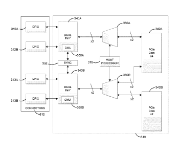
[0010] Figure 3 is
a block diagram illustrating an example of a host
interface with dual physical interfaces (dual PHYs) that may be used with one
or
two root complexes.
[0011] Figure 4 is
a block diagram illustrating an example of a host
system in communication with a PCIe card via a x8 PCIe link.
[0012] Figure 5 is
a block diagram illustrating an example of a host
interface with a combination of dual PHYs and a quad PHY that may be used
with one or two root complexes.
DETAILED DESCRIPTION
[0013] While
certain embodiments of the inventions are described,
these embodiments are presented by way of example only, and are not intended
to limit the scope of the inventions. Indeed, the novel methods and systems
described herein may be embodied in a variety of other forms. Furthermore,
various omissions, substitutions and changes in the form of the methods and
systems described herein may be made without departing from the spirit of the
inventions.
Overview
[0014] As described above, Peripheral Component Interconnect
Express (PC1e) compliant devices may come in a variety of sizes and forms.
Further, the PCIe standard may be used with a variety of types of devices
including solid state drives and graphics cards. Generally, PCIe compliant
devices come with a number of components that are application specific.
2
CA 02915056 2015-12-10
WO 2014/201178
PCT/US2014/042007
However, despite being application-specific, many PCIe complaint devices may
share similar types of components. For example, a number of PCIe compliant
devices may include a host interface that is designed to facilitate
communication
between the host system via one or more root complexes and the PCIe device.
Although some PCIe compliant devices share component types, each
component is separately designed because the sub-components may be
application specific and do not enable flexibility of use.
[0015] Some
embodiments of the present disclosure relate to host
interface designs that provide the flexibility to be used with a variety of
PCIe
compliant devices, which may have varying number of associated root
complexes. In some embodiments, the flexible host interfaces can reduce one or
more costs associated with a PCIe device. This reduced cost can be achieved in
some cases despite increasing the flexibility of the host interfaces.
[0016] Some
embodiments presented herein utilize physical interfaces
(PHYs) of varying sizes and, in some cases, PCIe cores of varying sizes
thereby
enabling the host interface to be used with a variety of systems and PCIe
topologies. For example, some embodiments described herein may be used with
host devices that have one, two, or more root complexes without redesigning
the
host interface for each host. The PHYs disclosed herein may include PCIe
PHYs.
[0017] Although, to
simplify discussion, the present disclosure is
described in terms of PC1e, the disclosure is not limited as such. For
example,
the present disclosure may be utilized with any type of serial interface,
including
a high speed serial interface. Further, the present disclosure may be used
with
any type of device and/or card that includes a serial interface and one or
more
processing cores.
System Overview
[0018] Figure 1A is
a block diagram illustrating an example of a host
system 102 in communication with a storage device 104 via a x4 PCIe link. In
one embodiment, the storage device 104 may be a SSD, a hard disk drive, a
3
CA 02915056 2015-12-10
WO 2014/201178
PCT/US2014/042007
hybrid disk drive, or any other data storage device. The host system 102 may
include any computing device that may communicate with a storage device. As
shown, the host system 102 may include a root complex 106 that communicates
with the storage device by communicating with a System on Chip (SoC) 108 of
the storage device 104. The root complex 106 can include any system that can
facilitate processing memory access commands by, for example, generating
transaction requests on behalf of a process. The storage device 104 can
include
any type of storage media that may include one or more non-volatile solid
state
memory arrays 160 (illustrated in Figure 1B). In some embodiments, other types
of media such as rotating magnetic media may be used in place of, or in
addition
to, the solid state memory. The SoC 108 can include one or more components
for interacting with the storage device 104 and the non-volatile solid state
memory arrays 160.
[0019] Further
details of the storage device 104 and the SoC 108 are
illustrated in Figure 1B, which is a block diagram illustrating a more
detailed
example of the host system 102 in communication with the storage device 104.
As shown in Figure 1B, the host system 102 may include a processor 132 in
addition to the root complex 106. The processor may issue memory access
commands and handle data traffic to/from the storage device 104. In some
cases, the root complex 106 may act as an intermediary by allowing the
processor 132 to off-loading at least partial processing of memory access
requests to the root complex 106. Although
illustrated as two separate
components, in some cases, the root complex 106 may be included as part of
the processor 132.
[0020] As
previously stated, the storage device 104 may include a
number of non-volatile solid state memory arrays 160. The arrays may comprise,
for example, flash integrated circuits, Chalcogenide RAM (C-RAM), Phase
Change Memory (PC-RAM or PRAM), Programmable Metallization Cell RAM
(PMC-RAM or PMCm), Ovonic Unified Memory (OUM), Resistance RAM
(RRAM), NAND memory, NOR memory, EEPROM, Ferroelectric Memory
(FeRAM), or other discrete NVM chips. The solid state storage devices may be
physically divided into blocks, pages and sectors, as is known in the art.
Other
4
CA 02915056 2015-12-10
WO 2014/201178
PCT/US2014/042007
forms of storage (e.g., battery backed-up volatile DRAM or SRAM devices,
magnetic disk drives, etc.) may additionally or alternatively be used.
[0021] The storage
device 104 may include connectors 112 that
communicate signals from the root complex 106 to the SoC 108 and vice versa.
The connectors 112 may be physical connectors, such as PCIe connectors or
differential input/output connectors. The signals may include both memory
access commands and data.
[0022] In some
cases, the SoC 108 may function as a controller. The
SoC 108 may include at least a host interface 110 and a memory controller 114.
Although not shown, the SoC 108 may include additional components that
facilitate the management of and access to the non-volatile solid state memory
arrays 160. For example, the SoC 108 may include Error Correcting Code (ECC)
systems.
[0023] The host
interface 110 can include any system for receiving
signals from the root complex 106 via the connectors 112 and preparing the
signals for processing by the memory controller 114. These signals may include
memory access commands and data for storage in the non-volatile solid state
memory array 160. Further, the host interface 110 may be configured to process
signals received from the memory controller 114 for provisioning to the root
complex 106. In some cases, the host interface may include a host processor
116. The host processor 116 may include any system that can facilitate the
processing of signals received at the host interface 110. More details
regarding
the host interface 110 are described below with respect to the Figure 1C.
[0024] The memory controller 114 can include any system for
communicating with the non-volatile solid state memory array 160. The memory
controller 114 may access the non-volatile solid state memory array 160 in
response to memory access commands received from the host interface 110.
Further, the memory controller 114 may perform memory management
commands such as garbage collection and wear leveling. In some
embodiments, the memory controller 114 may include a processor 120 for
performing some or all of the memory management and memory access
commands.
CA 02915056 2015-12-10
WO 2014/201178
PCT/US2014/042007
[0025] Figure 1C is
a block diagram illustrating a more detailed
example of the host interface 110 illustrated in Figure 1B. The host interface
110, in addition to the host processor 116 illustrated in Figure 1B, may
include a
quad PHY 140 and a x4 PCIe core 142. The quad PHY 140 is a PHY that can
support four lanes. Each pin of the quad PHY may communicate with a PCIe
lane associated with a connector 112A-112D of the connectors 112. As
illustrated in Figure 1C, each connector 112A-112D of the connectors 112 may
be a lane that includes two differential signaling pairs (e.g., E10/11 and
E13/14,
E19/20 and E22/23, etc.). One of the differential signaling pairs may be used
for
transmitting data and/or commands and one of the differential signaling pairs
may be used for receiving data and/or commands. Although four connectors
112A-112D and a single quad PHY 140 is illustrated, it is possible for the
number of connectors and the number of quad PHYs to differ. For example, the
host interface 110 may include two quad PHYs, with each quad PHY in
communication with four connectors for a total of eight connectors.
[0026] The quad PHY
140 can include any type of physical interface
configured to receive signals from the connectors 112 and perform a number of
signal processing operations before providing the signals to the PCIe core
142.
For example, the quad PHY 140 may reshape, regenerate, filter, or perform
other
signal processing functions. Further, the quad PHY 140 may alter the frequency
of the received signal. In some cases, the quad PHY 140 may take a serial
signal and convert it to a parallel signal. For example, the quad PHY 140 may
take a high-speed serial stream of data and convert it into a lower-speed
parallel
stream. Once the signal has been processed, the quad PHY 140 may provide
the signal to the PCIe core 142.
[0027] In some
embodiments, the signal may be modified to match an
industry standard, such as the PHY Interface for PCI Express (PIPE) published
by Intel . Advantageously, by implementing the PIPE standard, PHYs and PCIe
cores developed by different manufacturers can be configured to function with
each other. In some cases, the PIPE standard may be implemented by the quad
PHY 140 and the PCIe core 142. However, in other cases, an intermediary, such
as the PIPE 144, may be used to modify the signals sent and received to or
from
6
CA 02915056 2015-12-10
WO 2014/201178
PCT/US2014/042007
the quad PHY 140 and/or the PCIe core 142 to enable successful
communication between the quad PHY 140 and the PCIe core 142. Although
illustrated as a separate device in the Figure 1C, typically the PIPE 144 is a
conceptual device representing the format of signals for communication between
devices. In other words, the requirements of the PIPE 144 device may be
implemented as part of the quad PHY 140 and the PCIe core 142 rather than as
a separate component of the host interface 110.
[0028] As mentioned
above, the host interface 110 may include a x4
PCIe core. The x4 PCIe core may include any type of PCIe core that can
facilitate communication between a root complex and a controller, such as the
memory controller 114. The PCIe core may perform a number of digital signal
processing (DSP) functions to facilitate the communication. For example, the
PCIe core may perform error correction, request retransmission of requests,
packetize received data, establish a data link later, etc.
Example of a Multi Root Complex System
[0029] While in
some cases multiple root complexes may share a PCIe
core, generally, each root complex and/or processor uses or is associated with
a
separate PCIe core. Thus, the example presented in Figure 10 illustrates a
host
interface 110 that is configured for use with a host system 102 that includes
a
single processor 132 and/or root complex 106. However, as illustrated in
Figure
2A, a host system 202 may include multiple root complexes.
[0030] Figure 2A is
a block diagram illustrating an example of a host
system 202 with two root complexes 206A, 206B in communication with a
storage device 204 via a pair of x2 PCIe links. The storage device 204 may
include a SoC 208, which may have similar functionality as the SoC 108
previously described. As with the SoC 108, the SoC 208 may function as a
controller for the storage device 204.
[0031] Figure 2B is
a block diagram illustrating an example of a host
interface 210 that may be included in the System on Chip (SoC) 208 of Figure
2A. The host interface 210 may communicate with the root complexes 206A,
206B via connectors 212, which may be used to connect the SoC 208 to the
7
CA 02915056 2015-12-10
WO 2014/201178
PCT/US2014/042007
storage device 204. The connectors 212 may be physical connectors and may
include some or all of the embodiments previously described with respect to
the
connectors 112. As with the connectors 112, the connectors 212 may include
four connectors with each connector including a lane of two differential
signaling
pairs as described with respect to the connectors 112A-112D. However, unlike
the connectors 112A-112D, the four connectors of the connectors 212 may be
split into two pairs of connectors, connectors 212A, 212B and connectors 213A,
213B.
[0032] Each pair of
connectors 212A, 212B and 213A, 213B may be
assigned to or associated with a different root complex 206A, 206B. In other
words, in some cases, each pair of connectors 212A, 212B and 213A, 213B may
be configured to receive signals from and transmit signals to a different root
complex 206A, 206B. Further, as
illustrated in Figure 2B, each pair of
connectors 212A, 212B and 213A, 213B may communicate with a different quad
PHY 240A, 240B. The connectors 212A, 212B may communicate with the quad
PHY 240A and the connectors 213A, 213B may communicate with the quad PHY
240B.
[0033] Each quad PHY 240A, 240B may communicate with a x4 PCIe
core 242A, 242B respectively. Thus, the root complex 206A may provide data
and/or a command to the connectors 212A, 212B, which is provided to the PCIe
core 242A via the quad PHY 240A. Similarly, the root complex 206B may
provide data and/or a command to the connectors 213A, 213B, which is provided
to the PCIe core 242B via the quad PHY 240B. Further, the PCIe cores 242A,
242B may communicate with the root complexes 206A, 206B respectively via the
quad PHYs 240A, 240B and corresponding connectors 212A, 212B and 213A,
213B respectively.
[0034] As
illustrated in Figure 2B, in some cases when a host system
202 includes multiple root complexes 206A, 206B, portions of the quad PHYs
240A, 240B and the PCIe cores 242A, 242B may be underutilized or not utilized
at all. For example, the pins 0 and 1 of the quad PHY 240A of Figure 2B may be
in communication with connectors 212A, 212B, but pins 2 and 3 may remain
unconnected or may be terminated. Likewise, pins 2 and 3 of the quad PHY
8
CA 02915056 2015-12-10
WO 2014/201178
PCT/US2014/042007
240B may remain unconnected or may be terminated. Further, although four
connections are indicated in Figure 2B between the quad PHYs 240A, 240B and
the PCIe cores 242A, 242B, only two of the connections may be utilized. In
some embodiments, only two connections may be formed between the quad
PHYs 240A, 240B and the PCIe cores 242A, 242B. In such cases, the ports
and/or functioning blocks associated with the excess capacity of the quad PHYs
240A, 240B and the PCIe cores 242A, 242B may be deactivated, terminated, or
otherwise rendered in operable, or may function but may be unused. Although
not illustrated, similar to the host interface 110, the host interface 210 may
include a host processor.
[0035] In certain
embodiments, enabling the host interface 210 to be
used with a host system 202 that includes multiple root complexes may result
in
wasted resources, such as energy, space, and money. Further, in some cases,
using quad PHYs results in reduced flexibility with respect to the application
of
the host interface 210. One solution to the reduced flexibility and the wasted
resources is to use PHYs of different sizes with a host interface. For
example,
using dual PHYs instead of quad PHYS, or in combination with quad PHYs, can
reduce the amount of wasted resources and increase the flexibility of the host
interface. Examples of alternative host interfaces are presented below with
respect to Figures 3 and 5.
Example Host Interface with Dual PHYs
[0036] Figure 3 is
a block diagram illustrating an example of a host
interface 310 with dual physical interfaces (dual PHYs) 340A, 340B that may be
used with one or two root complexes (e.g., root complexes 206A, 206B). The
host interface 310 may include similar functionality as the host interface
210. For
example, as with the host interface 210, the host interface 310 enables
communication between two root complexes and two PCIe cores.
[0037] Generally,
the host interface 210 is not used with a single root
complex. In cases where the host interface 210 is used with a single root
complex, the host interface 210 may be limited to two PCIe lanes (e.g., via
the
connectors 212A, 212B). However, the host interface 310 may be used with a
9
CA 02915056 2015-12-10
WO 2014/201178
PCT/US2014/042007
host that includes a single root complex. Further, the host interface 310 may
provide a host with a single root complex (e.g., the host 102) with access to
four
PCIe lanes via the connectors 312A, 312B, 313A, 313B.
[0038] The host
interface 310 may communicate with one or more root
complexes of the host via the connectors 312. As indicated in Figure 3, the
connectors 312 may be differential input/output connectors. As with the
connectors 212, the connectors 312 may be split into two pairs of connectors,
connectors 312A, 312B and connectors 313A, 313B.
[0039] Further, as
with the connectors 212, each pair of connectors
312A, 312B and 313A, 313B may be configured to communicate with or
associated with a different root complex (e.g., root complexes 206A, 206B). In
other words, in some cases, each pair of connectors 312A, 312B and 313A,
313B may be configured to receive signals from and transmit signals to a
different root complex 206A, 206B. Further, as illustrated in Figure 3, each
pair
of connectors 312A, 312B and 313A, 313B may communicate with a different
dual PHY 340A, 340B. The connectors 312A, 312B may communicate with the
dual PHY 340A and the connectors 313A, 313B may communicate with the dual
PHY 340B.
[0040] As with the
host interface 210, the host interface 310 may
include a pair of PCIe cores 342A, 342B. In the illustrated embodiment, the
PCIe
core 342A is a x4 PCIe core 342A that is capable, in some cases, of processing
signals received at the host interface 310 from up to four connectors 312A,
312B,
313A, 313B. Further, the PCIe core 342B is a x2 PCIe core that is capable, in
some cases, of processing signals received at the host interface 310 from up
to
two connectors 313A, 313B. The PCIe cores 342A, 342B in the example
illustrated in Figure 3 have been selected to enable the host interface 310 to
support a single root complex accessing a x4 PCIe core, or two root complexes,
each capable of accessing a separate PCIe core.
[0041]
Advantageously, in certain embodiments, the host interface 310
provides greater flexibility compared to the host interface 210 because the
host
interface 310 can be used with both a host system that includes one root
complex and a host system that includes two root complexes. Further, when
CA 02915056 2015-12-10
WO 2014/201178
PCT/US2014/042007
used with a host system that includes a single root complex, the host
interface
310 enables the root complex to use four lanes of the x4 PCIe core. Moreover,
the host interface 310 uses smaller PHYs thereby wasting less resources (e.g.,
money, size, power) than the host interface 210 while supporting greater
functionality and flexibility than the host interface 210.
[0042] Figure 3
presents one example configuration of the host
interface that uses a minimal number and size of PCIe cores while supporting
both single root complex and dual root complex host systems. However, other
configurations are possible. For example, both PCIe cores 342A, 342B may be
x4 PCIe cores. As a second example, the PCIe core 342A may be a x4 PCIe
core and the PCIe core 342B may be a x8 PCIe core.
[0043] Each dual
PHY 340A, 340B includes a clock multiplier unit
(CMU) 350A, 350B. The CMUs 350A, 350B can include any system capable of
modifying a clock signal received externally from the host interface 310 or
received externally from the dual PHYs 340A, 340B. For example the clock
signal may be received from a pin input (not shown) to the host interface 310.
As
a second example, the clock signal may be received at the controller from an
external source or from a clock generator and provided to the host interface
310.
Regardless of where the clock signal is received, the CMUs 350A, 350B may
modify the clock signal by increasing or decreasing the frequency of the clock
signal. In some embodiments, the CMUs 350A, 350B may be omitted and/or
non-active.
[0044] The host
interface 310 may also include a synchronizer 352, or
sync, configured to synchronize the clock signal provided to the dual PHYs
340A,
340B. In some embodiments, the synchronizer 352 may synchronize the clock
signal provided to the dual PHYs 340A, 340B by controlling the CMUs 350A,
350B. Controlling the CMUs 350A, 350B may include synchronizing the
operation of the CMUs 350A, 350B. Alternatively, the synchronizer 352 may
synchronize the clock signal by selecting a CMU (e.g., the CMU 352A) to modify
the clock signal for both dual PHYs 350A, 350B and by deactivating the non-
selected CMU (e.g., the CMU 352B). In some cases, the synchronized clock
signal may be provided to other devices included in the host interface 310,
such
11
CA 02915056 2015-12-10
WO 2014/201178
PCT/US2014/042007
as the PCIe cores 342A, 342B and the host processor 316. In some
embodiments, the synchronizer 352 may be omitted and/or non-active. For
example, in cases where the host system includes two root complexes,
synchronizing the clock signals may be unnecessary as each root complex may
provide commands/data asynchronously. However, in some cases, despite
multiple root complexes functioning asynchronously from each other, the
synchronizer 352 may still synchronize the clock signals and/or CMUs 350A,
350B to maintain synchronous memory access of non-volatile solid state memory
array(s).
[0045] With further
reference to Figure 3, the host interface 310 may
include one or more selectors and/or multiplexors 360A, 360B. The selectors
360A, 360B direct a signal received from the dual PHYs 340A, 340B,
respectively, to the selected PCIe core 342A, 342B. As illustrated in Figure
3,
signals received from the dual PHY 340B may be provided to either the PCIe
core 342A or the PCIe core 342B based, at least in part, on a selector signal
received at the selector 360B from the host processor 316. Signals from the
dual
PHY 340A may be provided to the PCIe core 342A.
[0046] As
illustrated by the single connection between the selector
360A and the PCIe cores, in some cases, signals from the dual PHY 340A are
provided to the PCIe core 342A regardless of a selector signal. In such cases,
the host processor 316 may not communicate with the selector 360A. Further, in
some such cases, the host interface 310 may not include the selector 360A.
However, in other cases, as illustrated in Figure 3, the selector 360A is
included
regardless of the selection being from a set of PCIe cores of size one.
Advantageously, in certain embodiments, including the selector 360A enables
the host interface 310 to maintain an equal or substantially equal
communication
latency between the dual PHY 340A and the PCIe core 342A, and the dual PHY
340B and the PCIe core 342B. In some alternative embodiments, the selector
360A may be replaced by a latency block, which may be created from one or
more delay elements (e.g., flip flops), that is configured to provide an equal
or
substantially equal amount of latency as is introduced into the signal path
12
CA 02915056 2015-12-10
WO 2014/201178
PCT/US2014/042007
between the dual PHY 340B and the PCIe cores 342A, 342B by the selector
360B.
[0047] The host
processor 316 may generate or provide the selection
signal to the selectors 360A, 360B based on firmware, which may be pre-
installed or pre-configured. In some cases, an external signal provided to the
host interface 310 may be provided as the selector signal to the selectors
360A,
360B. Alternatively, the external signal may be used by the host processor 316
to determine the selector signal. In some embodiments, the selector signal may
be automatically determined in response to the host system in communication
with the host interface 310. For example, if the host system includes one root
complex, the host processor 316 may provide a selector signal to the selector
360B causing the selector to provide signals received from the dual PHY 340B
to
the PCIe core 342A.
Alternatively, if the host system includes two root
complexes, the host processor 316 may provide a selector signal to the
selector
360B causing the selector to provide signals received from the dual PHY 340B
to
the PCIe core 342B. In some cases, the host interface 310 is preconfigured. In
such cases, the PCIe core that receives signals from a PHY does not change
during operation.
[0048] In some such
cases, regardless of the number of root
complexes included with the host, the selector signal will not change. For
example, suppose that the host interface 310 has been preconfigured for use
with a host that includes two root complexes. In such a case, signals received
from one root complex will be communicated to connectors 312A, 312B, on to
the dual PHY 340A, and then on to the PCIe core 342A via the selector 360A.
Similarly, signals received from the second root complex will be communicated
to
connectors 313A, 313B, on to the dual PHY 340B, and then on to the PCIe core
342B via the selector 360B. Continuing the above example, now suppose that a
host with a single root complex is connected to an SSD with the host interface
310. In such a case, the connectors 312A, 312B may receive signals from the
root complex, but the connectors 313A, 313B may receive no signals and the
dual PHY 350B and the PCIe core 342B may not be utilized. In other cases,
13
CA 02915056 2015-12-10
WO 2014/201178
PCT/US2014/042007
both PHYs 340A, 340B and PCIe cores 342A, 342B may receive instructions and
data from the single root complex.
Example PCIe Card
[0049] Embodiments
of the present disclosure so far have been
described with respect to a storage device such as a solid state drive.
However,
the disclosure is not limited as such. The present disclosure can be applied
to
other PCIe based devices, such as a PCIe card (e.g., a PCIe graphics card, a
PCIe network card, a PCIe USB card, etc.). Figure 4 is a block diagram
illustrating an example of a host system 402 in communication with a PCIe card
404 via a x8 PCIe link.
[0050] As with the
storage device 104, the PCIe card 404 may include
a SoC 408 that communicates with a root complex 406 of the host system 402.
The SoC 408 may be configured similarly to the SoC 108. In other words, the
SoC 408 may include a host interface and a controller, which may or may not be
a memory controller based on the type of PCIe card. Further, the host
interface
of the SoC may be configured to use different size PHYs thereby enabling the
PCIe card 404 to be utilized with other host systems that may include multiple
root complexes. An example, of the host interface for an SoC 408 of a PCIe
card
404 that may be used with multiple root complexes is illustrated in Figure 5.
Example Host Interface for a PCIe Card
[0051] Figure 5 is
a block diagram illustrating an example of a host
interface 510 with a combination of dual PHYs 540A, 540B and a quad PHY
5400 that may be used with one or two root complexes. The host interface 510
may include similar functionality as the host interfaces 310, 210. For
example,
as with the host interfaces 210, 310, the host interface 510 enables
communication between two root complexes and two PCIe cores.
[0052] Further, as
with the previously described host interfaces, the
host interface 510 may communicate with one or more root complexes via a set
of connectors 512. The connectors 512 may be divided into a number of sets of
connectors based on a number of root complexes of the host system and/or
14
CA 02915056 2015-12-10
WO 2014/201178
PCT/US2014/042007
PHYs included in the host interface 510. For example, the connectors 512 may
include connectors 512A, 512B associated with a dual PHY 540A and
connectors 513A, 513B associated with a dual PHY 540B. Both pairs of
connectors 512A, 512B and 513A, 513B may be configured to communicate with
a first root complex. The connectors 514A-514D, which may be associated with
a quad PHY 5400 may be configured to communicate with a second root
complex. Alternatively, connectors 512A, 512B, 513A, 513B, 514A-514D may
be configured to communicate with a single root complex.
[0053] Further, the
host interface 510 may include some or all of the
components as previously described with respect to the host interfaces 210,
310.
For example, as illustrated in Figure 5, the host interface 510 may include a
number of PHYs including the dual PHYs 540A, 540B and the quad PHY 5400.
Each PHY 540A, 540B, 5400 may include a CMU 550A, 550B, 5500
respectively. The CMUs 550A-5500 may be configured to multiple or modify a
clock signal received at each of the PHYs 540A-5400. As with the host
interface
310, some or all of the CMUs 550A-5500 may or may not be active based on a
number of factors, such as the number of root complexes of the host system
and/or the CMU selected as a master CMU. The master CMU may control
modification, or multiplication, of clock signals for each PHY. In some cases
the
remaining CMUs may be inactive. In other cases, the remaining CMUs may be
slave CMUs that modify clock signals for corresponding PHYs based on
instructions from the master CMU, which may itself receive instructions or be
controlled by a synchronizer.
[0054] As with the
host interface 310, the host interface 510 may
include synchronizers 552A, 552B for synchronizing the clock signals received
at
the PHYs 540A-5400. Although two synchronizers are illustrated in Figure 5, in
some embodiments, the host interface 510 may include a single synchronizer
that is configured to synchronize some or all of the CMUs 550A-5500 and/or
clock signals received at the PHYs 540A-5400. The synchronizer can
synchronize the CMUs 550A-5500 and/or clock signals of the PHYs 540A-5400
using some or all of the previously described processes with respect to the
synchronizer 352. For example, the synchronizers 552A, 552B may synchronize
CA 02915056 2015-12-10
WO 2014/201178
PCT/US2014/042007
the clock signals of all three PHYs 540A-5400, when a single root complex is
used in the host system. Alternatively, such as in some cases when two root
complexes are included in the host system, the root complex 552A may
synchronize the clock signals of the PHYs 540A, 540B. In some such cases, the
synchronizer 552B may control the CMU 5500 of the PHY 5400. Alternatively,
the synchronizer 552B may be inactive.
[0055] With further
reference to Figure 5, the host interface 510 may
include a pair of PCIe cores 542A, 542B. By including two PCIe cores 542A,
542B, the PCIe card (or SSD card) that includes the host interface 510 can be
utilized with systems that include one or two root complexes. In some
embodiments, the host interface 510 may be configured to include an
alternative
number of PCIe cores. For example, the host interface 510 can be configured
with three PCIe cores, thereby enabling the host interface 510 to be used with
hosts that include three root complexes. In such an example configuration, one
or more of the selectors may be configured to select between three PCIe cores.
Further, although the PCIe cores 542A, 542B are illustrated as x4 and x8 cores
respectively, other size cores are possible. For example, both PCIe cores
542A,
542B could be x8 cores.
[0056] As
previously indicated, the host interface 510 may include a
number of selectors 560A, 560B, which may select between PCIe cores 542A,
542B based on a control signal, which may be received from the host processor
516 or from an external control signal. Further, the host interface 510 may
include a latency unit 562 that is configured to provide the same or
substantially
similar latency between the quad PHY 550 and the PCIe core 542B as is
provided by the selectors 560A, 560B. In some cases, the latency unit 562 may
include any components or devices that can add to or control latency in a
signal.
For example, the latency unit may include one or more flip flops or latches.
In
some embodiments, as described with respect to Figure 3, the latency unit 562
may be a selector that selects from a single PCIe core, or which has its
selection
function deactivated.
[0057] Although not
illustrated, in some embodiments, the latency unit
562 may receive a control signal or other signal to facilitate the latency
unit 562
16
CA 02915056 2015-12-10
WO 2014/201178 PCT/US2014/042007
maintaining a latency consistent with the latency introduced by one or more of
the selectors 560A, 560B. This control signal, or other signal, may be
provided
by the host processor 516 or otherwise. In some cases, the latency unit may
receive signals from before and after one or the sectors enabling the latency
unit
to determine an appropriate latency to apply to a signal received from the
quad
PHY 5400. For instance, if the
latency unit determines that a previous
instruction provided to the selector 560B took four clock cycles to be passed
through the selector 540B to the PCIe core 542B, the latency unit 562 may
introduce a latency of four clock cycles to signals received from the quad PHY
5400.
Conclusion
[0058] Disclosed
systems and methods enable a host interface to be
utilized with multiple applications. The host interface can include multiple
PHY
sizes and configurations that enable a PCIe based solid state drive and/or
PCIe
card to be used with hosts with varying numbers of processors and/or root
complexes. Further, the host interface can include multiple PCIe cores with
varying sizes and configurations that enable a PCIe based solid state drive
and/or PCIe card to be used with hosts with varying numbers of processors
and/or root complexes. Accordingly, increased flexibility and reduced cost
(e.g.,
monetary cost, energy cost, space cost) is obtained for designing and
manufacturing different SSD and PCIe card applications and configurations.
Other Variations
[0059] Those skilled in the art will appreciate that in some
embodiments, other approaches and methods can be used. For example, in
some embodiments, each PHY may be associated with its own PCIe core and
multiple PHYs may be associated with a single root complex. In such a case,
the
selectors may be optional. Additional system components can be utilized, and
disclosed system components can be combined or omitted. Depending on the
embodiment, certain of the steps described above may be removed, others may
be added.
17
CA 02915056 2015-12-10
WO 2014/201178
PCT/US2014/042007
[0060] While certain embodiments of the disclosure have been
described, these embodiments have been presented by way of example only,
and are not intended to limit the scope of the disclosure. Indeed, the novel
methods, devices and systems described herein may be embodied in a variety of
other forms. Furthermore, various omissions, substitutions and changes in the
form of the methods and systems described herein may be made without
departing from the spirit of the disclosure. The accompanying claims and their
equivalents are intended to cover such forms or modifications as would fall
within
the scope and spirit of the disclosure. For example, those skilled in the art
will
appreciate that in various embodiments, the actual physical and logical
structures
may differ from those shown in the figures. Depending on the embodiment,
certain steps described in the described examples and processes may be
performed in different order, removed, and others may be added. Also, the
features and attributes of the specific embodiments disclosed above may be
combined in different ways to form additional embodiments, all of which fall
within the scope of the present disclosure. Although the present disclosure
provides certain preferred embodiments and applications, other embodiments
that are apparent to those of ordinary skill in the art, including embodiments
which do not provide all of the features and advantages set forth herein, are
also
within the scope of this disclosure. Accordingly, the scope of the present
disclosure is intended to be defined only by reference to the appended claims.
18