Note: Descriptions are shown in the official language in which they were submitted.
81793387
1
Direct imprinted panel with two-layer-structure
1. Field of the invention
The present invention relates to a panel, particularly to a wall, ceiling, or
floor panel with an
improved surface primer as well as a method for manufacturing it.
2. Background of the invention
A plurality of panels for wall, ceiling, and/or floor coatings are known from
the prior art. For
example, so-called laminate panels are widely spread as floor coating in the
inner area.
Laminate panels are relatively cheap and can be well processed. Commonly, they
are based on
a carrier plate made of MDF or HDF material, on which a decor paper,
impregnated with
to melamine resin, is applied to its upper side. By grouting under
influence of heat and pressure,
the resins cure, such that a highly abrasion-resistant surface is formed. To
increase abrasion
resistance, the surface is often provided with abrasion resistant particles,
in particular
corundum, prior to grouting.
As an alternative to laminate panels, for some time past, high-quality panels
based on PVC are
known and are distributed as LVT (luxury vinyl tiles). For example, a floor
panel in the form
of multi-layered, rectangular laminate with a carrier plate consisting of soft
polyvinylchloride
(PVC) is known from DE 10 2006 058 655 Al. Onto the soft PVC layer, or plate
respectively,
a decor paper web is glued on, such that the visible surface of the PVC is
applied with a decor.
As an alternative to such decor paper webs, applied to a PVC carrier plate,
also the usage of
plastic foils is known, which are also, for example, imprinted with a
decorative decor.
From DE 10 2006 029 963 Al, a floor coating made of polyvinylchloride is
known, which is
coated with a durable lacquer layer, to improve durability of the PVC floor
coating. The
lacquer layer is based on an acrylate resin and is cured by means of
radiation. The core of this
document relies in adding of electrical conductive substances to the resin,
for proving the
finished floor coating with antistatic and/or electrical conductive
properties.
More recently, LVT panels prevailed on the market that have a harder PVC plate
with a
thickness of 4-6 mm as a ground and on which a soft PVC layer is applied,
comprising the
CA 2915134 2017-10-12
= 81793387
2
features as described above. Specific profiles are milled into the harder
plate as coupling
means. In such a way, the single panels can easily be laid to form a plane
area.
In a further development of the above described panels, so-called direct
imprinted panels have
been developed. Commonly, for these direct imprinted panels no more papers of
foils are
used, in particular no decor paper. The decor layer is rather directly
imprinted onto the surface
of the carrier plate, to which commonly a suitable pretreatment is applied, by
utilizing
dispersion colors by means of an intaglio printing process. In particular,
before printing, a
primer is applied by means of roller application. After drying of the decor
layer, various resin
layers are applied and cured. The resin layers thereby serve as a protective
layer as well as
to abrasion resistant surface. To further improve abrasion resistance,
often abrasion resistant
particles, like corundum, are provided, too.
From WO 2007/042258, for example, a method for direct coating of wood
materials is known,
in which a thick protective layer made of plastic material is applied liquidly
onto the surface
of a plate within one coating step. The used plastic material is a liquid,
polymerizable acrylate
system that is cured by polymerization.
The mentioned prior art panels each have several pros and cons, depending from
their
structure, from the used manufacturing process, and from the used materials.
For example,
laminate panels can easily be laid, provide the opportunity to realize high-
quality decors, and,
additionally, are very durable. However, typically, the acoustic properties of
laminate panels
are disadvantageous, which produce annoying running noise when used as a floor
coating.
Responsible for that is the very hard melamine layer on the laminate surface.
In addition, this
melamine layer is felt as cold and unpleasant. Coatings based on PVC have
excellent acoustic
properties and, additionally, have a pleasant haptic and feel relatively soft
and warm, which is
desirable in many cases, e.g. when used as a floor coating in a bathroom.
However, for
producing optical high-quality surfaces, such PVC floorings have to be
processed in a relative
costly manner, and are therefore significantly more expensive compared to
common laminate
panels, at least when they should provide comparable quality. A disadvantage
of PVC panels
is that deep scratches can easily arise on the soft surface when intensively
used, which disturb
the optical image. Furthermore, it is disadvantageous that PVC floorings are
not harmless
CA 2915134 2017-10-12
81793387
3
from the ecological point of view. They comprise harmful plasticizers and
chlorine is known
as very dangerous in case of fire (e.g. chlorine dioxin development).
Direct imprinted panels remove some of the disadvantages of laminate panels
and, e.g., need
no decor paper soaked with melamine resin, whereby the manufacturing may be
simplified.
However, compared to laminate panels, they have similar disadvantages with
regard to
acoustic properties and haptic.
3. Summary
In light of these known panels, or respectively coatings, an objective is to
provide a panel,
particularly a wall panel, a ceiling panel, or a floor panel, comprising as
much as possible of
to the different advantages of the known panels, but at the same time,
however, minimizing the
existing disadvantages of the various panels. In addition, the further
objective is to
manufacture such a panel in a cheap and relatively simple manner. A further
objective is
providing such panels that have a good durability and which allow to realize
high-quality
decorative patterns.
According to an aspect of the present disclosure, there is provided a panel,
comprising a
carrier plate having a front side and a back side, wherein the carrier plate
comprises a layer
system at least at the front side, wherein the layer system, originating of
the front side,
comprises: a first elastic layer Si made of an aliphatic polymer, having a
thickness of 20
to 600 um and a Martens hardness M51 of 0.5 to 120 N/mm2; as well as a second
layer S2
made of a polymer, having a thickness of 10 to 180 um and a Martens hardness
M52, wherein
Ms2> Ms ; and a decor layer arranged between the front side and the layer Si,
comprising a
printing ink based on one or both of: polymerizable acrylate and N-
vinylcaprolactam; wherein
the printing ink of the decor layer and at least a part of the layer S1 have
been hardened
together by radiation.
There is also provided a method for manufacturing a panel, comprising the
following steps in
the given order: (a) providing a carrier plate; (b) applying a primer and
imprinting a decor
layer thereon; wherein the decorative pattern is imprinted by means of a
polymerizable
printing ink based on one or both of: a polymerizable acrylate and N-
vinylcaprolactam; and
CA 2915134 2017-10-12
= 81793387
4
the printing ink and the at least one applied coat of liquid radiation
hardenable aliphatic
acrylate are cured together by radiation; (c) applying a coat of liquid
radiation hardenable
aliphatic acrylate, having a Martens hardness Ms1 of 0.5 to 120 N/mm2 after
curing; (d) at
least partially curing of the in step (c) applied coat of liquid radiation
hardenable aliphatic
acrylate by means of radiation; (e) optionally repeating the steps (c) and (d)
until a first elastic
layer Si with a thickness of 20 to 600 IL.tm exists; (f) applying a coat of
liquid radiation
hardenable acrylate, having a Martens hardness Ms2 after curing, wherein Ms2 >
MSI; (g) at
least partially curing the in step (f) applied layer of liquid radiation
hardenable aliphatic
acrylate by means of radiation; (h) optionally repeating the steps (f) and (g)
until a second
to layer S2 exists, having a thickness of 10 to 180 um.
In some embodiments, the panel is not provided with abrasion-resistant
particles, in particular
aluminium oxide particles.
In some embodiments, the layer system has a damping effect of at least 5 dB,
preferably at
least of 8 dB, and most preferably of at least 9 dB, compared to the uncoated
carrier plate,
measured according to F,PI,F norm.
In some embodiments, the hardness of the elastic layer Si is substantially
constant over the
total thickness, and in that the hardness differences within the layer are
particularly less than
N/mm2, preferably less than 15 N/mm2, and more preferably less than 10 N/mm2.
According to the present invention, a panel, like a wall, ceiling, but
particularly a floor panel
20 is provided that comprises a carrier plate with a front side and a back
side, wherein at least a
layer system is applied at the front side. The front side shall be understood
as the side which is
the used side that points to the observer, when the panel is laid, e.g., in
form of a floor. The
carrier plates can optionally be divided into panels. At their side edges, the
panels can provide
coupling means, particularly in form of tongue and groove elements, as known
from the area
of floor laminate panels. Particularly suited tongue and groove elements allow
connecting
various similar panels in parallel direction to the front side and also
perpendicular to the front
side by form fitting. Of course, the process sequence can be applied to the
panels one by one,
wherein this approach is less economical. The layer system, according to the
invention,
originating of the front side, comprises a first elastic layer made of a
polymer and which is
CA 2915134 2017-10-12
81793387
called layer S1 in the following. This first polymer layer according to the
invention having a
thickness of 20-600 lam and a Martens hardness Msi of 0.5-120 N/mm2,
preferably between 2
and 50 N/mm2, more preferably between 2 and 40 N/mm2, and most preferably
between 2 and
30 N/mm2, and it is soft elastic. Above this first elastic layer, a second
layer S2 is provided
5 that has a thickness of only 10-200 [tm and a Martens hardness M52 which
is greater than the
Martens hardness of the first elastic layer. i.e. Ms? > M51. The Martens
hardness Mv),
determined at the panel surface, is between 5-300 N/mm2, preferably at
15-150 N/mm2, more preferably between 20 and 100 N/mm2, and most preferably
between 25
and 90 N/mm2.
The structure of the layer system of the panel according to the invention
implicates that the
surface of a coated panel in such a way ¨ independent from the material of the
carrier
plate¨feels relatively soft and has for human feelings a comfortable warm
haptic impression.
In particular, providing a thick elastic layer Si has significant acoustic
advantages. Compared
to a laminate reference floor, the layer system according to the invention
leads to a significant
noise damping effect when walked on. According to IHD-W 431, a loudness of 26
Sone is
determined for a laminate reference floor. The floor, provided with an elastic
layer Si and a
layer S2 comprises an improvement of 10-70% compared to this reference floor.
A PVC
(LBT) floor was measured with an improvement of 40% compared to the reference.
A plurality of different materials is possible as materials for the carrier
plate since the relevant
physical properties of the panel according to the invention are substantially
determined by the
applied layer system. Thus, generally, the carrier plate of the panel
according to the invention
is preferred with a MDF plate, an HDF plate, a PVC plate, a cement fiber
plate, a WPC plate
(wood powder composite), a thermoplastic recycling plate, a wood plate, a wood
veneer plate,
or a parquet plate like a pre-fabricated parquet plate. As mentioned at the
beginning, the
carrier plate may comprise coupling means in form of tongue and groove
elements at its sides,
such that the panels according to the invention can, for example, be easily
laid to form a
covering on a floor.
In general, materials for the layers S1 and S2 (and S3) are preferably based
on acrylate
systems or based on acrylates, respectively. An acrylate system is herein to
be understood as a
CA 2915134 2017-10-12
81793387
6
polymerizable mixture of mono-, hi- and multi-functional acryl acid based
compounds
comprising double bonds. Typical representatives are, for example,
dipropylenglycoldiaerylate, 1,6-hexandioldiacrylate, polyurethane acrylate
acid ester,
polyester-acrylate acid ester as available on the market according to the
production program
of the company BASF under the trademark LaromerTM types.
Layer S1 is preferably a polymer based on a radical polymerizable oligomer
and/or oligomer
mixture. Preferably, it is based on radiation hardenable acrylate oligomers
(acrylate system).
The oligomers are chosen such that the layer provides damping properties,
characterized in
that the Martens hardness is preferably 0.5-120 N/mm2, more preferably 2-50
N/min2. Such an
oligomer formulation consists, for example, of one or more unsaturated
acrylates that
comprise a polyester, polyether and/or a polyurethane structure, with a
functionality of 1-4,
preferably < 2. Commercially available examples are the Laromer PO 43 F, the
Laromer UA
9033 or the Laromer UA 19 T of BASF. Additionally, the oligomer mixture may
comprise
low viscose acrylate ester with a functionality of 1-4, preferably with a
functionality of 1-2.
Commercially available examples are the Laromer LR 8887, Laromer DPGDA,
Laromer
TPGDA of BASF. For hardening by means of UV-radiation, photo initiators like
mono- or
bi-sacylphosphinoxide, alphahydroxycetone, benzophenon derivate,
benzildimethycetal or
phenylglyoxalate are needed. In addition, the formulation can comprise
additives like wetting
agents, defoamers, inorganic or organic filling materials. As additives, for
example, poly
acrylate, silicones, talcum, barium sulfate, chalk, silicic acid or polyuria
derivates may be
used.
The material of the second layer S2 is preferably based on a radical
polymerizable acrylate
oligomer (acrylate system) or a radical polymerizable acrylate mixture,
consisting of one or
more unsaturated acrylates (aeryl ate system), a polyester, polyether and/or
polyurethane
structure with a functionality of 1-8, preferably 3-6. Examples are the
Laromer PE 9074,
Laromer 8863 or Laromer LR 8987 as raw lacquer materials of BASF. Preferably,
these
acrylate mixtures further comprise low viscose acrylate ester with a
functionality of 1-6,
preferably with a functionality of 2-4. For example, following raw materials
of BASF with the
trademark name Laromer HDDA, Laromer TMPTA, Laromer PPTTA can be used. In case
of
UV-linked systems, photo initiators as for example mono or
bisecylphosphinoxide,
CA 2915134 2017-10-12
81793387
7
alphahydroxycetone, benzophenon derivate, benzildimethylcetal or
phenylglyoxylate are
applied. Furthermore, additives like wetting agents, defoamers, matting agents
and inorganic
or organic filling materials may be applied, like poly acrylate, silicones,
talcum, barium
sulfate, chalk, silicic acid or polyuria derivates. The oligomers are chosen
such that the
surface hardness lies in the above-mentioned ranges. Furthermore, the raw
material selection
is made such that the layer S2 has, besides damping properties, in particular,
a high abrasion
resistance (scratch resistance, micro scratch resistance, abrasion
resistance). The skilled
person knows that these properties are achieved by network density and
modifications, for
example, with nano particles.
Preferably, the thickness of the carrier plate is between 3 and 20 mm, more
preferably
between 4 and 15 mm and even more preferably between 3 and 12 mm, and most
preferably
between 4 and 10 mm. Depending on the usage and the applied decor (if
available), different
shapes are possible. If, for example, the panel shall imitate a real wood
decor and be laid as a
floor panel or wall panel, a square base form of the carrier plate or the
panel is advantageous,
e.g. in a square shape of 1.5-2 m in length and 10-30 cm in width.
As mentioned at the beginning, the relevant physical properties of the surface
of the panels
according to the invention are substantially determined by the layer system
according to the
invention. The thick first elastic layer S1 is decisive for the acoustic
properties of the panels.
Basically, preferred hardness values according to Martens for the layer Si are
between, as
90 mentioned above, 0.5-120 N/mm2, more preferably between 2-50 N/mm2, even
more
preferably between 2-40 N/mm2 and most preferably between 2-30 N/mm2. In every
case, the
second layer S2 must have a greater hardness compared to the first layer and
should be, as
mentioned above, in a range between 5-300 N/mm2, more preferably at 15-150
N/mm2 and
more preferably between 20-100 N/mm2 and most preferably between 25-90 N/mm2.
The
skilled person knows that even if the mentioned ranges for the preferred
hardness of Msi and
M52 partially overlap, it is substantially in the focus that M52 is greater
than Mst.
Determining the Martens hardness is known by the skilled person. During
development of the
present invention a Taber Abraser measurement device 5151 of Taber Industries
was used.
Every 200 rounds with an abrasive paper S41 the hardness and the track depth
was determined
CA 2915134 2017-10-12
81793387
8
of the probes. Determination of the Martens hardness (registered hardness
control under test
force influence) was conducted according to DIN EN ISO 14577. As a measurement
device, a
"Fischerscope H100" of the Helmut Fischer GmbH was used. Following test
parameters have
been used: maximum force: 50/30 mN and measurement duration: 20 seconds. The
determination of the track depth has been conducted with a mechanical touch
cut
measurement device. As a measurement device a perthometer S3P of the company
Perthen
was used.
During surveying the probes, it has been shown that probably due to the
relatively soft used
materials more or less large deviations in the hardness of a given layer depth
occur. Thus, it is
necessary to measure at various points to achieve meaningful representative
data by
calculating average values. During the conducted measurements, the hardness
and the track
depth have been each measured at four locations, after 200 rounds of the
abrasive paper. It
appears, in most cases that four measurement points provide sufficient
accuracy. Of course,
even more precise measurement results will be achieved when more than four
measurement
points are used, e.g. eight.
Preferably, the thickness of the elastic layer Si is in range of 20-600 um,
more preferably of
40-500 um, even more preferably of 80-450 um, and most preferably of 120-240
um. The
second layer S2 has, independently of the thickness of the first layer,
preferably a thickness of
10-180 um, more preferably of 20-100 tim and most preferably of 30-80 um.
Thereby, it is
apparent for the skilled person, the thicker the first elastic layer Si is
chosen, the more elastic
the properties of the surface of such coated panels arc. The layer S1 is
preferably applied one
after another in part steps, particularly by means of various roller devices
with respective
gelling after the roller application devices. Gelling is understood that in
the respective layer a
radical polymerization is initiated by radiation, e.g. by means of UV, but
this polymerization
is cancelled fast, such that the adhesion of the following layers is ensured.
In other words, the
part layers are each not completely cured, but only in part. In this way,
among other things,
also the adhesion of the part layers to each other is increased. The layer S1
can, alternatively,
be applied in one single step.
CA 2915134 2017-10-12
81793387
9
Preferably, a further decor layer is applied between the front side and the
layer SI, comprising
a printing ink (ink) or consists of this printing ink, respectively. The term
"printing ink" is
herein used generically and shall not denote a single color, but printing ink
in a generic
fashion: with regard to digital four-color printing, the printing ink, for
example, consists of
four different colors (cyan, magenta, yellow, black), of which the printing
image is generated
by spraying on ink drops. When using indirect intaglio printing, the decor
image, as is known,
is generated by means of rotating printing cylinders. By means of the printing
cylinders, decor
specific mixture colors are applied. In principle, with respect to the present
invention, it is
preferred that the layers SI and S2 are substantially transparent such that
they can serve as
to protection for an underlying decor layer.
Commonly, dispersion colors are used as printing ink in the prior art, in
particular acrylate
colors. These dispersion colors are regularly utilized by the commonly used
intaglio printing
process. Dispersion colors are printing inks that normally consist of three
main components,
namely a) a dissolver (commonly water), b) a bonding agent in form of plastic
polymers that
are stored together and form a solid layer when the solvent evaporates, and c)
color pigments
for generating the desired cover and the desired color tone. The hardening of
these dispersion
colors is not performed by means of polymerization, but by evaporation of the
solvent, since
the bonding agents already exist in terms of polymers. The polymers included
in the
dispersion connect themselves by means of evaporation of the bonding agents in
a purely
physical manner and form a solid, closed layer.
Surprisingly, it has been found out in connection with the present invention
that improved
adhesion properties of the layer systems according to the invention can be
achieved, when, in
the present case, instead of usual dispersion colors, polymerizable printing
inks are used. The
positive effect is particularly remarkable when the printing ink of the decor
layer and at least
in part of the first elastic layer S1 are cured or polymerized together,
respectively (when the
decor layer is directly imprinted, as e.g. with digital printing, the decor
layer consists of the
printing ink, so to speak). Curing or partially curing (gelling) of a polymer
layer or a
polymerizable printing ink is to be understood as a chemical reaction in which
a
polymerization takes place. This has to be distinguished from drying of such
layers, wherein
only the solvent, like the water content of a dispersion color, evaporates or
is reduced in a
CA 2915134 2017-10-12
81793387
purely physical manner. By means of the combined (partial) curing of the
polymerizable
printing ink and the materials for the first elastic layer, probably a
chemical linking occurs
that the border surface of both layers, of which it is assumed that it is
responsible for the
improved adhesion of the layers. The commonly used dispersion colors do not
comprise
5 polymerizable acrylate systems such that no chemical linking between the
printing ink, i.e. the
decor layer, and the elastic layer takes place.
Generally, the printing inks used for the present invention are therefore
preferably
polymerizable printing inks and in particular polymerizable acrylate systems.
Polymerizable
printing inks comprise as main component bonding agents, namely reactive
double bondings
to containing resins; monomers or oligomers, like acrylate monomers and
acrylate oligomers;
optionally photo initiators for radiation hardenable printing inks; additives
like defoamers,
flow additives and the like; and color pigments and filling material for
achieving specific
physical technical properties. Generally, the used printing inks for the
present invention are
preferably radiation hardenable, particularly by UV ray hardenable printing
inks. More
preferably, the printing ink is based on a polymerizable acrylate and/or N-
vinylcaprolactam.
In a further embodiment according to the invention, a third elastic layer S3
is provided on the
front side beneath the decor layer which has a Martens hardness M53, wherein
the hardness of
the third elastic layer is preferably equal or less than the hardness of the
first elastic layer Sl,
i.e. Ms3 < Msi. In this way, particularly thick layer systems with
corresponding good elastic
properties may be generated. Preferably, the layer S3 should have a thickness
of 10-300 [irn,
more preferably of 30-150 [irn and most preferably of 60-120 m. For the layer
S3, a radical
polymerizable acrylate mixture is used, as it is provided for the layer Si and
described above.
This oligomer mixture is preferably applied with pigments before application
in order to
provide the layer with a covering color as printing ground, i.e. that this
layer S3 should
preferably not be transparent in order to achieve a sufficient printing
quality. The decor layer,
including possible necessary primers and primary coatings, is then applied
onto the before
applied layer S3. The advantage of this third layer S3 is that the total layer
system can be
designed very thick without impacting the optical impression of an eventually
present decor
layer since only the first elastic layer Si and the second layer S2 lie
between the observer and
the decor layer.
CA 2915134 2017-10-12
81793387
11
The layer system according to the invention has the advantage that no further
paper or plastic
foils are necessary at the front side of the panel or the carrier plate, as it
has been necessary in
many applications in the prior art. Therefore, the panels can be applied with
a layer while
running through a machine and do not have to be stuck together with a before
produced paper
or plastic foil.
In a further embodiment according to the invention, the decor layer, including
the possibly
necessary support layers like primers or coating primers can be arranged
between layer Si and
the wear layer S2.
In addition, the present invention also relates to a process for manufacturing
a panel,
to particularly a panel as discussed above. In this process, a carrier
plate, like a MDF or HDF
carrier plate, is provided in a first step. The carrier plate is applied with
a layer of liquid
radiation hardenable acrylate such that is selected that after successfully
curing, it provides a
Martens value Msi of 0.5-1201\1/mm2. With common roller application processes
normally
layer thicknesses of up to 80 m, and in special cases up to 100 p.m can be
applied in one
working step. In order to achieve the desired layer thicknesses for the first
elastic layer Si, it
will be commonly necessary to harden each applied layer, preferably by means
of radiation in
order to apply a further layer on this partly or completely cured layer. Since
preferably always
the same materials are used, a homogenous elastic ¨ according to the hardness
¨ layer Si with
a thickness of up to 600 p.m can be generated. However, for each of the layers
of layer Sl,
different materials with different values for Ms1 can be used, which, however,
should
preferably not differ too much from each other and should in every case be in
the range
according to the invention of 0.5-1201\1/mm2. Particularly, an as much as
possible
homogeneous hardness in the final layer Si (or S2) is preferred, which can
most easily be
achieved by using the same or at least similar materials. After achieving the
desired final
thickness of the elastic layer S I, after Si has been partially or completely
cured, a layer with
further liquid radiation curable acrylates is applied, wherein this is chosen
such that the layer
comprises a Martens hardness M52 after curing, which is greater than the
Martens hardness of
the before applied first elastic layer. Also in this case, it might be
necessary to apply various
layers with respective connected (part-) curing steps, if a particularly large
final thickness of
the second layer S2 is desired. Although in this case different materials can
be used for every
CA 2915134 2017-10-12
81793387
12
layer of the layer S2 with different values for Ms?, as long as (every) Msi is
less than the
smallest Ms2 of the single layers of the layer S2. However, also here it is
preferred to use the
same or at least similar materials for the partial layers of the layer S2,
since this improves the
cohesion of the partial layers and may lead to an increased durability of the
total layer S2
(respectively Si).
Advantageously, before applying the first elastic layer Si onto the surface of
the carrier plate,
a primer is applied and a decor layer is imprinted thereon. Preferably, this
is done by direct
printing, wherein the above in connection with the panel according to the
invention described
technical information are also basically usable for the present method. In
other words, the
to decor layer or the decorative pattern is here also preferably applied by
means of a
polymerizable printing ink and more preferably at least a first layer of the
first elastic layer Si
is applied onto the not yet (at least not completely) cured printing ink and
then cured together
with the printing ink. In this manner, a particularly good connection of the
layer system with
the surface of the carrier plate is achieved.
Example 1:
In a first step, an HDF carrier plate with a thickness of 8 mm is applied with
a primer based on
a commercial watery acrylate dispersion with an application of 10 g/m2 by
means of a roller
application device. In a next step, smoothing of the plate by means of a
roller application
device by means of a filler based on a highly filled watery acrylate
dispersion with an
application amount of 25 g/m2 is done. Afterwards, a printing ground (primer
coating) based
on a watery acrylate dispersion enriched with filling materials and color
pigments is applied
by means of a molding process (i.e. by a curtain coating process) with an
amount of 70 g/m2.
After each of these coating steps, an intermediate drying at a temperature
between 80-200 C
is performed. The plates treated in such a way are then applied to a printing
machine,
substantially consisting of a gravure roller and a rubber roller used for
transferring the printing
image from the gravure cylinder onto the plate. The printing image is
generated by means of
three down-streamed printing devices, wherein by means of each of the printing
devices an
own dispersion printing ink, consisting of color pigments and a watery
acrylatc dispersion is
applied. For an imitation of a dark nut tree wood, for example, 5 g/m2 of
printing ink are
CA 2915134 2017-10-12
81793387
13
applied. In a further process, a commercial UV primer is applied onto the
printing color layer
by means of a roller application device. By means of a subsequent roller
application device, a
radical polymerizable acrylate oligomer mixture (1) is applied in an amount of
80 g/m2. This
oligomer mixture (1) comprises 70 parts of Laromer PE 9032 and 25 parts of
Laromer TBCH
of BASF, as well as five parts of further additions (benzildimethylcetal as a
photo initiator, an
aliphatic urethane acrylate with a functionality of 3). By means of a UV
emitter, gelling
(partially curing) is performed for this layer. By means of a further roller
application device,
again the same (or alternatively a similar) oligomer mixture (1) in the amount
of 80 g/m2 is
applied and at least in part cured. Onto the in such a way built first elastic
layer S1 a layer S2
to with a further double bonding containing, with photo initiators enriched
radiation hardenable
oligomer (2) in an amount of 50 g/m2 is applied by means of a third roller
application device
and is polymerized by means of UV radiation. This oligomer (2) consists of a
mixture of 75
parts of Laromer PE 9074, 20 parts Laromer HDDA of BASF and 5% of further
additives
(among other things phenylglyoxalate as photo initiator) and has a greater
hardness (Ms2)
compared to the first layer Sl.
Example 2: Panels for which the printing image is generated by means of
radiation hardened
printing inks.
Again, it is used an 8 mm thick HDF carrier plate and, according to example 1,
it is provided
with a watery primer, filler and printing ground. On the plate, treated in
such a way, the same
decor image according to example 1 is generated by means of a digital printer.
However,
hereby no dispersion colors are used, but UV radiation hardenable digital
printing inks. For
generating the printing image, an amount of about 2 g/m2 of ink is needed. At
first, the ink is
fixed with 150 mJ/cm2 (mercury) and then, the first layer of layer S1
according to the first
example is applied and together with the printing ink cured at least in part
(gelled). The
further steps are then performed according to example 1.
CA 2915134 2017-10-12
81793387
14
Example 3:
An HDF carrier plate undergoes the production steps up to behind the printing
machine
according to example 1. Onto the dried printing ink, a commercial watery UV
primer is
applied. By means of the preceding process, the plate is heated up to a
surface temperature of
50-60 C, such that water of the primer evaporates fast such that the primer
is fixed.
Subsequently, an oligomer mixture (1) according to example 1 is applied in an
amount of 50
g/m2 by means of a roller device and gelled by means of UV radiation.
Afterwards, a second
roller application of 50 g/m2 of that oligomer mixture (1) (or a similar one)
with a subsequent
gelling and, finally, a third application (1) of 50 g/m2 with subsequent
gelling in order to form
to the layer Si. Then, by means of a roller application device, the wear or
covering layer (i.e.
layer S2) of 30 g/m2 is applied and hardened by means of UV radiation. The
oligomer (2') for
the covering layer S2 consists of a mixture of 75 parts Laromer PE 9074, 20
parts Laromer
HDDA of BASF and 5% of further additives (among others, phenylglyoxalat as
photo
initiator and a matting agent). By means of the amount of the added matting
agent, the desired
t5 degree of gloss of the surface is controlled. The further processing of
the plates into floor
panels is preformed according to example 1.
Example 4:
In a first step, an HDF carrier plate with a thickness of 8 mm is applied with
a primer based on
a commercial watery acrylate dispersion with an application of 10 g/m2 by
means of a roller
20 application device. In a next step, smoothing of the plate by means of a
roller application
device by means of a filler based on a highly filled watery acrylate
dispersion with an
application amount of 25 g/m2 is performed. Subsequently, a UV radiation
hardenable mass in
an amount of 40 g/m2 is applied by means of a roller device. This radiation
hardenable mass
consists of 65 parts of the oligomer mixture (1) according to example 1 and of
35% finest
25 dispersed titanium dioxide. Subsequently, it is gelled by means of UV
radiation. A second
application of 40 g/m2 of this mass is performed by means of a down-streamed
roller
application device with subsequent gelling. The resulting layer is in
accordance with the
above-described layer S3. Afterwards, digital printing according to example 2
is conducted.
Furthermore, optionally, a commercial UV primer in an amount of 3 g/m2 is
applied by means
CA 2915134 2017-10-12
= 81793387
of a roller application device. The further coating with the oligomers (1) and
(2) used for
generating the layers Si and S2 is performed according to example 1 and also
the
manufacturing of the panels of the base plates.
Subsequently, some determined properties of the manufactured floor materials
according to
5 the examples 1-4 are presented:
a) Determining the walking noise emission according to IHD-W 431
(version of
May 14, 2012)
The characteristic values have been determined with non-compliance of the
spectrums with
the biggest and smallest noise unit (outlier correction according to II ID-W
431). The result is
to shown in terms of a difference between the A-rated total sound pressure
level and the noise
unit of the examined variance compared to the reference floor. The changing of
the linear
parameter noise unit (N) is determined according to the reference in percent
as follows:
Change in percentage:
((Nref¨ * 100 %)/Nref
15 The determined characteristic value shows the increase (negative value)
or decrease (positive
value) in percent of the loudness experience. The reference is a common
laminate floor with a
melamine resin coating and a plate thickness of 8 mm.
Table 1: A-rated total sound pressure level
Version Reference Probe Improvement
(mid-range extent
(mid-range
spectrum) [dBA
(A)] spectrum) [dBA [dBA (A)]
(A)]
Example 1 75,3 64,8 10,5
Example 2 75,3 65,2 10,1
CA 2915134 2017-10-12
= .81793387
16
Example 3 75,3 65,5 9,8
Example 4 75,3 64,3 11,0
LVT (PVC) 75,3 64,9 10,4
floor (5 mm in
thickness)
The examples show that a significant noise reduction during walking can be
achieved by
means of the coating according to the invention. A reduction of 10 dB is felt
like a halving of
the loudness by means of the human hearing. To have a direct comparability,
only HDF
carrier plates have been used as carrier plates in the examples 1-4. With
alternative carrier
plates further significant noise reductions are possible.
4. Description of preferred embodiments
In the following, the present invention is explained in more detail with
reference to the
attached figures. At this:
io Fig. 1 a and b show an exemplary layer structure of a schematic
illustration; and
Fig. 2 shows an exemplary system for manufacturing of the panel according to
the invention
in a schematic view.
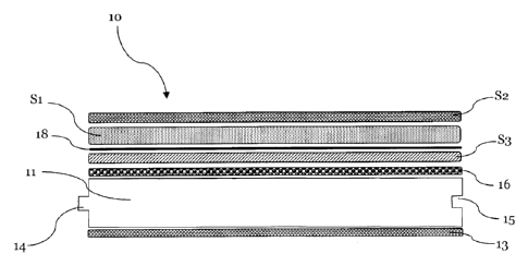
In Fig. la, a schematic layer structure of a panel 10 according to the
invention is shown. The
illustration is purely schematic and not true to scale. In particular, the
carrier plate 11 is
significantly thicker compared to the further layers 12-18, which lie in a
range of some
hundred um. Furthermore, the single layers are shown in an explosion view in
order to
simplify the understanding and are in a real case directly adjacent to each
other or directly
arranged above each other. In the shown example, a carrier plate 11 with a
thickness of about
8 mm made of an HDF material is shown. At the backside of the carrier plate 11
a moisture
barrier 13 in form of an appropriate plastic foil is pasted. The moisture
barrier is optional and
depending on the material of the carrier plate 11 and the desired usage area.
A carrier plate 11
CA 2915134 2017-10-12
81793387
17
furthermore comprises coupling means in form of tongue 15 and groove elements
14, which
are only shown schematically in Fig. la (and b). Suitable coupling means in
form of tongue
and groove elements that allow connecting various similar panels in parallel
direction of the
front side and also perpendicular to the front side by means of form fitting
are known by the
skilled person. Commonly, at the four sides of a square or quadrangle carrier
plate opposing
complementary coupling means are provided. Details about such coupling means
or locking
profiles are known by the skilled person from the technology of laminate floor
production, as
e.g. known from the document WO 0188306 or from the document WO 0148332 of the
same
applicant, which are hereby entirely incorporated by reference.
In the shown layer system of panel 10, a primer coating 16 with a thickness
of, for example,
50-200 p.m is provided which is based on a watery acrylate system. Beneath the
primer,
further very thin primer coatings and/or filler layers may be applied as known
by the skilled
person from the area of direct imprinted panels. A decor layer or a decor 18
is imprinted onto
the primer 16. The decor 18 or the decor layer 18 have been applied, for
example, by means of
a polymerizable printing ink by a digital four color printing. A first elastic
layer S1 is located
above the decor layer 18 with a thickness of 200 p.m and a Martens hardness
M51
of 15 N/mm2. A second layer S2 is applied onto the first elastic layer Si,
which has a
thickness of 80 p.m and a Martens hardness of about 25 N/mm2.
The example of Fig. lb corresponds to the example of Fig. la with the
difference that a
further elastic layer S3 is provided between the primer coating 16 and the
decor layer 18. The
layer S3 has preferably a Martens hardness Ms; which is less or equal than the
Martens
hardness of the layer Sl, therefore MS3 < MS1. In the example of Fig. lb, the
first layer Si
may be provided in a slightly thinner way compared to the example of Fig. la
which is shown
in both figures schematically by means of different thicknesses.
In the following, the manufacturing of a panel according to the invention is
exemplarily
shown in Fig. 2. Fig. 2 shows in a schematic way a coating system for coating
carrier plates
11. The carrier plates are trimmed and profiled after the coating in a
separate profiling line
(not shown). For example, the carrier plates 11 have a thickness between 3-20
mm, a length
(in transport direction of the system of Fig. 2) of 150-200 cm and a width of
125-210 cm.
CA 2915134 2017-10-12
81793387
18
However, any other plate dimensions can be used for the carrier plates, which
are cut in the
desired form and size at the end of the process. The stations shown in Fig. 2
of the system are
not to be understood conclusive, but only serve as an example explanation of
the methods
according to the invention. In front, behind and between the shown stations,
further
processing stations may be provided, like drying stations, stations for
applying primers,
stations for applying filler, control and monitor devices etc. The carrier
plates 11 are, for
example, transported through the coating system by means of roller conveying
device 20.
In the first shown station 30, a grounding mass is applied onto the front side
(main side) of the
carrier plates 11 by means of a liquid curtain 31 of coating material. The
liquid curtain 31
ranges among the complete width of the plate and the plates are transported
through this
curtain and are coated at the same time. Below the device 30 for outputting
the curtain, a
collection container 32 is located, in which the liquid curtain drops, when no
plate is passed
through the curtain, as for example, at a gap between two consecutive plates.
Preferably, a
watery acrylate dispersion is used as a coating material for the grounding. In
a subsequently
arranged drying station 40, the applied grounding is dried by means of hot
air, i.e. water is
extracted from the watery acrylate dispersion. After drying the grounding, a
decor layer is
imprinted onto the grounding by means of a digital printing device 45. This
decor layer, for
example, can imitate real wood, but nowadays commercial digital printing works
are able to
nearly print every desired decor or pattern on the plates. Preferably, a
printing ink is utilized
in printing device 45 that is polymerizable by means of radiation, i.e. a
printing ink that is
based on a polymerizable acrylate and/or N- vinylcaprolactam. It is apparent
for the skilled
person that the illustration of the digital printing device 45 is only purely
schematic and that
such printing devices commonly consist of several stations. After imprinting
the desired
decor, a first coating device 50 applies a first layer of liquid radiation
hardenable aliphatic
acrylate. The material is chosen in such a way that it comprises a Martens
hardness M51
of 0.5-120 N/mm2 after the curing. The device 50 is a roller application
device and is able to
apply a layer thickness of about 40-100 vim in one process step. In the
subsequent station 60,
the applied layer of liquid radiation hardenable aliphatic acrylate is cured
at least in part by
means of UV radiation. Subsequently, a second device 50' follows in order to
apply a second
layer of the same liquid radiation hardenable acrylate compared to the first
layer. Also here,
CA 2915134 2017-10-12
81793387
19
the station 50' is a roller application station which is commonly able to
apply layer
thicknesses of 30-100 tim. In station 60' this second layer is at least cured
in part by UV
radiation. Subsequently, in a third coating device 50" a third layer of the
same liquid radiation
hardenable acrylate is applied and in the third radiation station 60" it is at
least in part cured
by means of UV radiation. In the schematic view of Fig. 2 three such devices
are thus shown,
which are able to apply three layers in one layer, but however, also more or
less devices may
be available, depending on the desired total thickness of the first elastic
layer Si. In any case,
there is a first elastic layer S1 available at the exit of the last radiation
station 60" with a
thickness of about 150 tim. Then, onto this first elastic layer Sl, a layer of
liquid radiation
to hardenable acrylate is applied in an application station 70 that is
chosen in a way such that
after the curing it comprises a Martens hardness Ms2 that is greater than the
Martens hardness
of the first elastic layer and preferably at 5-300 1\l/mm2. Here, in Fig. 2,
as an example, only
an application device 70 and a station 71 for radiation hardening is shown,
but however, also
for the second layer S2 various devices may be provided, depending on the
desired final
thickness of the layer of S2. Then at the exit of the coating device, a coated
panel, according
to the invention will be available, that may be further processed as desired.
CA 2915134 2017-10-12