Note: Descriptions are shown in the official language in which they were submitted.
CA 02915406 2015-12-14
WO 2015/000593 PCT/EP2014/001822
1
A SUBSTRATE LESS DIE PACKAGE HAVING WIRES WITH DIELECTRIC AND METAL COATINGS
AND
THE METHOD OF MANUFACTURING THE SAME
15 Field of the Invention
The present invention relates to die packages with at least one die having a
plurality of connection pads and a plurality of leads extending from the
connection
pads, the leads having metal cores with a defined core diameter and a
dielectric
layer surrounding the metal cores having a defined dielectric thickness,
respectively.
Background
Electronic devices and components are operating at ever increasing speeds and
over increasing frequency ranges. Popular semiconductor package types use
wire bonds that can connect to a substrate or leadframe, which in turn can
connect to second level interconnects, vias, substrate or package traces,
solder
balls, or the like, for connection to a printed circuit board (PCB) of an
electronic
device.
However, packaging can be expensive, particularly if the substrate requires
costly
materials or precision drilling, etch, or formation of vias.
CA 02915406 2015-12-14
WO 2015/000593 PCT/EP2014/001822
2
Summary of the invention
Bearing in mind the problems and deficiencies of the prior art, it is an
object of the
present invention to provide a die package that can be manufactures easily and
with reduced overall production costs.
The above and other objects, which will be apparent to those skilled in the
art, are
achieved in the present invention which is directed to a die package
comprising a
die having a plurality of connection pads, a plurality of leads having metal
cores
with a defined core diameter, and a dielectric layer surrounding the metal
cores
having a defined dielectric thickness, at least one first connection pad held
in a
mold compound covering the die and the plurality of leads, the first
connection
pad being connected to the metal core of a first lead, and at least one second
connection pad held in the mold compound covering the die and the plurality of
leads, the second connection pad being connected to the metal core of a second
lead.
is The die package is preferably a "coreless" package without a permanent
substrate for die attachment. The die package according to the invention can
be
connected to a printed circuit board or to a substrate by means of solder
balls, for
example.
The first and/or the second connection pads can be held in the mold component
in such a way that they are exposed so that they can be connected to the PCB
or
to the substrate. In other words, the connection pads are held be the overmold
compound without being supported by a die substrate.
The first connection pad may be connected to the metal core of a first lead
and
the second connection pad may be connected to the metal core of a second lead,
whereas the first lead is longer than the second lead, has a different core
diameter and/or has a different dielectric diameter.
The die package can include several dies which may be arranged as stacked
dies. Further, at least one of the leads may be a ribbon lead formed by total
or
partial fusion of the dielectric coatings of two or more leads.
3
Further, the present invention is directed to a method of manufacturing a die
package according to the invention, the method comprising the following steps:
placing of one or more dies on a temporary workpiece including temporarily
attached pads, using wirebonding to connect the die to the temporarily
attached
pads, coating of metal cores of the wirebonds with a dielectric coating,
overmolding the die assembly and the leads, and removing at least part of the
temporary workpiece and/or at least part of the overmold to expose the
attached
pads for connecting them to a printed circuit board or another substrate, for
example by means of solder balls.
The method may further include one or more of the additional method steps
shown in Fig. 2.
According to the invention, "careless" semiconductor die packages can be
is produced. During manufacture, these die packages have leads attached
between
the die and pads on a temporary substrate. After the overmold, the temporary
substrate is removed to allow exposure of the lead attached pads, The leads
include a metal core surrounded by a dielectric. Preferably, they further
include a
metallized outer layer attached to ground pad connections.
Brief Description of the Drawings
Fig. 1 is an illustration of dielectric and metal coated leads in a coreless
package,
Fig 2 illustrates one embodiment of a method for manufacture of a careless
package,
Fig. 3 illustrates method steps for manufacture of dielectric coated leads
with
outer ground connected metallization useful In the embodiment illustrated with
respect to Fig. 1 and 2, and
Fig. 4 illustrates a subtractive method for manufacture of dielectric coated
leads
with outer ground connected metallization.
CA 2915406 2019-06-19
CA 02915406 2015-12-14
WO 2015/000593 PCT/EP2014/001822
4
Detailed Description
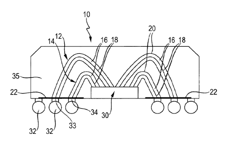
As seen in Fig. 1, a "coreless" package 10 without a permanent substrate for
die
attachment can be constructed. Such a semiconductor die packaging system can
be formed to have leads 12, 14 with a dielectric layer 16 deposited over an
inner
metal core 18, as well as an outer metal layer 20 deposited over the
dielectric
layer 16. In operation, the outer metal layer 20 is attached to a ground pad
22.
The leads 12, 14 are attached to die 30 that can include multiple connection
pads
for signal, power, or other functionality required by the die 30. In the
described
embodiment, the die 30 does not have to be attached to a permanent substrate.
Leads 12, 14 can connect to conductive pads 34, while the conductive pads can
be attached by means of solder balls 32, gold bumps, or other suitable
interconnects to a printed circuit board or other substrate. As illustrated,
the leads
12, 14 are surrounded by an epoxy or other mold packaging compound, and may
have substantially different lengths. In the illustrated embodiment, all leads
have
substantially the same impedance due to lead construction, even though lengths
may differ. However, in other embodiments the leads can be constructed to have
distinctly different impedances. For example leads that have a metal core of a
defined diameter along its length can be sequentially coated with a thin
dielectric
layer and a conductive metal layer. Such leads are suitable for transfer of
power
.. because the consequent low impedance reduces power sag. Alternatively,
leads
that have a much thicker dielectric layer are more suitable for transmission
of
signal data. In certain embodiments, due to the superior electrical
characteristics
of lead construction as disclosed, leads having substantially different
lengths but
the same core diameter can have substantially the same impedance, within 10%
of target impedance, despite having lengths that vary 50% or greater. In
certain
embodiments, lead differences can be even greater, with two leads having the
same cross sectional structure and impedance, but one lead being as much as
ten (10) times the length of the other. In still other embodiments, stacked
die are
contemplated, as are ribbon connections formed by total or partial fusion of
dielectric coatings forming the leads.
Fig. 2 is one embodiment of a method for manufacture of a coreless package
such as described with respect to Fig. 1. Multiple dies can be temporarily
CA 02915406 2015-12-14
WO 2015/000593 PCT/EP2014/001822
attached (40) to a workpiece that can be later physically released and
removed,
or otherwise etched or chemically eliminated. The workpiece includes
temporarily
attached pad to support both metal core and outer metal ground layer
attachment
of each lead. Wirebonding (41) is used to connect the die to the temporarily
5 attached pads surrounding the die, followed by a dielectric coating (42)
of the
metal core. The dielectric layer is metallized (43), with connections to
ground
pads being formed, and the entire multiple die assembly and leads are
overmolded (44). After curing of the overmold, the temporary workpiece is
removed (45), and the overmold may be etched or otherwise removed (46) by
grinding or polishing to better expose the lead attached pads. Individual die
and
their connected leads can be singulated, and readied for solder ball or other
connection to a printed circuit board (PCB) or another substrate (47).
Generally, thin dielectric layers will provide low impedance, suitable for
power
lines, thick dielectric is good for signal, and outer metal layers are
connected to
same ground. Note that a combination of core diameters and dielectric
thicknesses is possible and a series of such steps may be performed to achieve
more than two impedances. In certain embodiments it may be desirable to have
large cores on power lines to increase power handling capacity, reduce power
line temperatures, and/or further compensate any inductance on power supply
and ground lines that would exacerbate ground bounce or power sag. Dielectric
layers of intermediate thickness are also useful, since many packages could
benefit from having leads of three (3) or more different dielectric
thicknesses. For
example, a lead have an intermediate dielectric thickness could be used to
connect a source and load of substantially different impedance to maximize
power transfer. For example, a 10 ohm source can be coupled to a 40 ohm load
with a 20 ohm lead. Also, since cost of dielectric can be high, critical
signal
pathways can interconnected using thick dielectric, with less critical status,
reset,
or the like leads can be coated with a dielectric layer having a thickness
greater
than the power leads, but less than (intermediate) to the critical signal
leads.
Advantageously, this can reduces dielectric deposition material cost and time.
CA 02915406 2015-12-14
WO 2015/000593 PCT/EP2014/001822
6
The precise thickness of the dielectric coating may be chosen, in combination
with the wirebond diameter, to achieve a particular desired impedance value
for
each lead.
IT 1 3 8
Z 0 ¨ = ¨ = log (¨)
c a
( 1 )
The characteristic impedance of a coax line is given in Eq. (1), where L is
the
inductance per unit length, C is the capacitance per unit length, a is the
diameter
of the bond wire, b is the outside diameter of the dielectric and Er is
relative
permittivity of the coaxial dielectric.
As illustrated in Fig. 3, in one embodiment manufacture of dielectric coated
leads
with outer ground connected metallization can proceed using the following
steps.
Connection pads are cleaned (50) on the die and the substrate and a wirebonder
is used to connect the die to the connection pads (51). Optionally, a second
diameter wire can be attached (52) (e.g. a larger diameter wire suitable for
power
connections), or areas of the die can be masked (53) or otherwise protected to
allow for selective deposition. One or more layers of dielectric of the same
or
different composition can be deposited (54), followed by selective laser or
thermal
ablation, or chemical removal of portions of the dielectric to allow access to
ground connections covered in the dielectric deposition step (55). This step
is
optional, since in some embodiments, the need for a ground via can be
eliminated. This is particularly true for die operating at higher frequencies,
since
frequency dependence on thickness value (function of Er) allows for ground
establishment through capacitive coupling. Metallization (57) follows,
covering
the dielectric with a metal layer that forms the outermost metallized layer of
the
leads, and also connecting the leads to ground. The entire process can be
repeated multiple times (58), useful for those embodiments using selective
deposition techniques, and particularly for those embodiments supporting
multiple
die or complex and varied impedance leads. In the final step, for non-cavity
packages, an overmold can be used to encapsulate leads (59). Alternative
embodiments and additional or variant method steps are also described in
7
US20120066894 and US Patent 6,770,822_
In certain embodiments, modifications and additions to the described process
are
possible. For example, providing conformal coatings of dielectric can be
accomplished through a variety of methods using chemical (electrophoretic),
mechanical (surface tension), catalytic (primer, electromagnetic [UV, IR],
electron
beam, other suitable techniques. Electrophoretic polymers are particularly
advantageous because they can rely on self-limiting reactions that can deposit
precise thicknesses readily by adjusting process parameters and or simple
in additive, concentration, chemical, thermal, or timing changes to an
electrophoretic coating solution.
In other embodiments, dielectric precoated bondwires can be used to form
leads.
While commercially available coated wires typically are thinner in dielectric
thickness than is necessary to create, for example, 50 ohm leads, the
foregoing
discussed dielectric deposition steps can be used to increase dielectric
thickness
to set the desired impedance, Use of these precoated wires can simplify other
process steps necessary to create coaxes, and can allow for thinner layers of
needed vapor deposited dielectrics and faster processing times to create
ground
vias. Precoated bondwires can be used to prevent shorting for narrowly spaced
or crossing leads. In certain embodiments the precoated bondwire can have a
dielectric made from a photosensitive material to allow for selective
patterning
techniques.
In other embodiments, the dielectric paryiene can be used. Parylene is the
trade
name for a variety of chemical vapor deposited poty(p-xylylene)polymers used
as
moisture and dielectric barriers. Parylene can be formed in a growth limited
condensation reaction using a modified parylene deposition system where the
die, substrate, and leads are aligned to a photoplate which allows EM
radiation
(IR, UV or other) to strike in a precise manner causing selective growth rate
of
dielectric. Advantageously, this can minimize or eliminate the need for
processes
to create contact vies, bulk removal of parylene, etc.
CA 2915406 2019-06-19
CA 02915406 2015-12-14
WO 2015/000593 PCT/EP2014/001822
8
Parylene and other dielectrics are known to suffer from degradation due to
oxygen scission in the presence of oxygen, water vapor and heat. Damage can
be limited by metal layers that form excellent oxygen vapor barriers, with
thin
layers of 3-5 micron thickness capable of forming true hermetic interfaces.
Alternatively, if metal has been selectively removed, or not deposited in
certain
areas due to electrical, thermal, or manufacturing requirements, a wide range
of
polymer based vapor oxygen barriers can be used, with polyvinyl alcohol (PVA)
being one widely used polymer. These polymers can be glob topped, screen
printed, stenciled, gantry dispensed, sprayed onto parylene surface that will
be
exposed to the oxygen or H20 vapor environment. Advantageously, use of vapor
barrier polymers can be a part of a cost reduction strategy, since thicker
layers of
high cost parylene or other oxygen sensitive might otherwise be required.
As will be appreciated, all of the described method steps can benefit from
various
selective deposition techniques. Selective deposition can be by physical
masking,
directed polymer deposition, photoresist methods, or any other suitable method
for ensuring differential deposition thickness on the metal core, dielectric
layer, or
other outermost layer at time of deposition. While selective deposition allows
for
additive methods to build leads, it also allows for subtractive techniques in
which
dielectric or metal is removed to form multiple impedance interconnects. For
example, a package populated by one or more die can be wire-bonded as
appropriate for interconnect of all package and device pads. As seen with
respect
to Fig. 4, which illustrate steps and structures for manufacture of a die
package,
the dielectric coating 200 can be deposited (step A) to a thickness X-A over a
wirebond metal conductor 202, where A is the thickness of the dielectric
needed
for the secondary interconnect impedance. The secondary impedance wirebond
dielectrics can be removed (step B) for example by an etch step, followed by a
second coating 204 deposition (step C) followed by metallization 206 of both
interconnects (step D). This subtractive process will create wirebonds of two
distinct impedances.
In particular, the present invention is directed to a die package comprising a
die
having a plurality of connection pads, a plurality of leads having a metal
cores
CA 02915406 2015-12-14
WO 2015/000593 PCT/EP2014/001822
9
with a defined core diameter, and a dielectric layer surrounding the metal
cores
having a defined dielectric thickness, first connection pads held in a mold
compound covering the die and the plurality of leads connected to the metal
cores, and second connection pads held in a mold compound covering the die
and the plurality of leads connected to the metal cores.
The metal core diameters of the plurality of leads may differ in diameter.
The impedance of a subset of the plurality the leads may be within 10%.
Further, the invention relates to a method of manufacture the above die
package,
selected steps of the method being shown in Fig. 2 and elsewhere.