Note: Descriptions are shown in the official language in which they were submitted.
CA 02915407 2015-12-14
WO 2015/000594 PCT/EP2014/001823
AN INTERCONNECT SYSTEM COMPRISING AN INTERCONNECT HAVING A PLURALITY OF METAL
CORES AT LEAST PARTIALLY SURROUNDED BY A DIELECTRIC LAYER
15 Field of the Invention
The present invention relates to improved die-to-die or die-to-substrate
interconnects, including both discrete and same package die. Further, the
present
invention relates to trough lines for improved interconnection between sources
and loads with differing impedance.
Further, heat transfer interconnect structures that promote heat transfer away
from a die are described. Such interconnect structures are of particular use
in
multi-die and stacked die packages.
Background
Electronic devices and components are operating at ever increasing speeds and
over increasing frequency ranges. Popular semiconductor package types use
wire bonds that can connect to a substrate or leadframe, which in turn can
connect to second level interconnects, vias, substrate or package traces,
solder
balls, or the like, for connection to a printed circuit board (PCB) of an
electronic
device.
CA 02915407 2015-12-14
WO 2015/000594 PCT/EP2014/001823
2
However, leads might not have suitable mechanical properties, including
rigidity
and strength. In other embodiments, die pitch restrictions might not allow
distinct
leads coated by a non-overlapping dielectric layers, particularly when the
dielectric layers are thick.
Further, conventional package leads might not be optimized for particular
electrical characteristics including interconnects between sources and loads
with
differing impedance.
Additionally, as speed increases, so does power requirements and the need to
transfer waste heat away from the die. This is a particular problem for
stacked
die, interior die in a stack being effectively insulated on top and bottom by
substrate materials or other heat generating die.
Summary of the invention
Bearing in mind the problems and deficiencies of the prior art, it is
therefore an
object of the present invention to provide an interconnect system for
interconnecting semiconductor die packages with at least one die, the system
having improved mechanical properties of connection leads with minimal impact
on electrical characteristics.
Mechanical properties of leads for die packages are can be improved by fusion
of dielectric layers into metal coated ribbons, with minimal impact on
electrical
characteristics.
The above and other objects, which will be apparent to those skilled in the
art, are
achieved in the present invention which is directed to an interconnect system
for
interconnecting semiconductor die packages, comprising a first die having a
plurality of connection pads, and a ribbon lead extending from the first die,
the
ribbon lead having a plurality of metal cores with a core diameter, and a
dielectric
layer surrounding the metal cores with a dielectric thickness, with at least a
portion of dielectric being fused between adjacent metal cores along the
length of
the plurality of metal cores, and an outer metal layer attached to ground.
3
According to the invention, mechanical properties of leads for die packages
can be improved by
fusion of dielectric layers Into metal coated ribbons, with minimal impact on
electrical characteristics.
Further, trough lines can be created by partial or full fusion of dielectric
layers into partially or fully
coated metal ribbons. This allows for improved Interconnect between sources
and loads with
differing impedance, as well as better signal transfer characteristics to
package or substrate
mounted antenna, including patch antennas.
Further, heat transfer ribbon interconnect structures may promote heat
transfer away from a die.
Such ribbon interconnect structures are of particular use in multi-die and
stacked die packages.
The interconnect system May be a multi-die interconnect system comprising a
first die and a second
die, with each die respectively having a plurality of connection pads, the
ribbon lead extending from
the first die to the second die.
The interconnect system may be a through line interconnect system comprising a
first die and a
second die, with each die respectively having a plurality of connection pads,
the ribbon lead
extending from the first die to the second die.
The interconnect system may be a through line interconnect system with a
package substrate having
a plurality of connection pads, the ribbon lead extending from the package
substrate to the first die.
The outer metal layer may be exposed to ambient conditions to facilitate heat
transfer. Additionally
or alternatively, the ribbon lead may extend from the first die to a heat
sink,
Brief Description of the Drawings
Fig. 1 Is an illustration of a die to die Interconnect structure formed from
dielectric and metal coated
leads consolidated into ribbons for improved mechanical performance and
acceptable electrical
characteristics,
CA 2915407 2019-06-19
CA 02915407 2015-12-14
WO 2015/000594 PCT/EP2014/001823
4
Fig. 2 is an illustration of a large die to small die interconnect structure
formed
from dielectric and metal coated leads, with the leads consolidated into
ribbons
for at least a portion of their length due to reduced pitch of the smaller
die,
Figs. 3 and 4 respectively illustrate in plan and side view both package to
package and die to die interconnect with ribbon leads,
Fig. 5 illustrates method steps for manufacture of dielectric coated leads
with
outer ground connected metallization,
Fig. 6 illustrates a subtractive method for manufacture of dielectric coated
leads
with outer ground connected metallization,
Fig. 7 illustrates a BGA package having dielectric coated leads with outer
ground
connected metallization,
Fig. 8 illustrates a portion of leadframe package having dielectric coated
leads
with outer ground connected metallization,
Fig. 9 is an illustration of structures and methods for forming dielectric and
partially or fully metal coated leads optimized for interconnect requirements,
Fig. 10 illustrates in plan view two die interconnected by fully metallized
dielectric
coated leads merging into a partially metallized trough line,
Fig. 11 illustrates a packaged die to die trough line interconnect, and a
separate
trough line interconnect to a substrate mounted antenna,
Fig. 12 is an illustration of a die to die interconnect structure formed from
dielectric and metal coated leads consolidated into ribbons and exposed
outside
of a package for improved thermal transfer performance,
Fig. 13 is an illustration of a stacked die package including within package
die-to-
die and die-to external connection interconnect ribbon structures formed from
dielectric and metal coated leads for improved thermal transfer performance,
and
Figs. 14 and 15 respectively illustrate in plan and side view package to
package
ribbon interconnect with transfer to an active or passive heat sink.
CA 02915407 2015-12-14
WO 2015/000594 PCT/EP2014/001823
Detailed Description
As seen in Fig. 1, ribbon leads suitable for interconnecting semiconductor die
packages can be formed from leads having dielectric coated metal cores, with
the
dielectric coating completely or partially fused along the length of the lead.
The
5 dielectric coating is covered with outer ground connected metallization
to provide
the desired electrical characteristics while also improving mechanical
characteristics and resistance to polymer degradation through oxidation or
other
chemical effects. As seen with respect to Fig. 1, first and second die 1, 2
respectively having connection pads 3 are interconnected by two separate
1.0 .. ribbons 10, 20 composed of fused dielectric coating 15 that is
encapsulated with
metal. The process of forming a ribbon interconnect begins with attachment of
a
metal core 12 of a lead to die and substrate connection pads 3. The metal core
12 is coated with a dielectric 15 and metallized, with the metal being
connected to
a ground (possibly requiring a separate laser ablation or other step of
dielectric
removal to allow access to ground connection pads). For cavity packages, the
die
can be fitted with a hermetic lid or other cover. Otherwise the die can be
covered
with a mold compound, an epoxy glob top, or other suitable encapsulant
material,
separately (with the ribbon lead(s) extending out of the encapsulating
material, or
together in one multi-die package as required.
As seen in Fig. 2, ribbon leads suitable for interconnecting semiconductor die
packages can be formed from leads having dielectric coated metal cores 12,
with
the dielectric coating 15 only partially fused along the length of the lead.
In Fig. 2,
the smaller pitch of the smaller die results in fusion of dielectric material
near the
small die. This can reduce uniformity of electrical characteristics as
compared to
distinct and separated leads, since the electrical environment of edge leads
is
substantially different than interior leads, but the variation is minimal if
only a
limited length of the lead near the smaller die has fused dielectric.
Figs. 3 and 4 respectively illustrate in plan and side view a package-to-
package
connection using a ribbon lead 30 as discussed with respect to Fig. 1, as well
as
a die to die interconnection 32 in a common mold package, and a die-to-
substrate
CA 02915407 2015-12-14
WO 2015/000594 PCT/EP2014/001823
6
ribbon connection 34. As can be seen in Fig. 4, stacked packages 36 are also
supported, with ribbons extending between stacked die being shown.
In the following, the embodiments of the invention shown in Figs. 9 to 11 will
be
described: Partially metallized ribbon leads suitable for interconnecting
semiconductor die or other active or passive elements, including antenna, can
be
formed from leads having dielectric coated metal cores, with the dielectric
coating
completely or partially fused along the length of the lead. The dielectric
coating is
only partially covered with outer ground connected metallization to provide
the
desired trough line electrical characteristics. The process of forming a
ribbon
lo
interconnect begins with attachment of a metal core of a lead to die and
substrate
connection pads. The metal core is coated with a dielectric and metallized,
with
the metal being connected to a ground (possibly requiring a separate laser
ablation or other step of dielectric removal to allow access to ground
connection
pads).
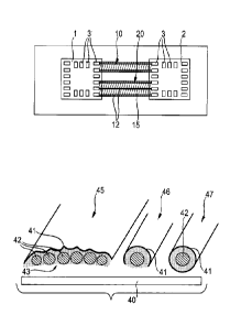
As seen in Fig. 9, leads 45, 46, 47 suitable for a semiconductor die package
are
positionable over a substrate 40, and can be formed from dielectric coated
metal
cores 42, with outer ground connected metallization 41. As seen with respect
to
Fig. 9, a non-uniform (or uniform in certain embodiments) dielectric coating
can
be selectively metallized to adjust electrical characteristics, including
impedance.
Selected partial metallization can occur with a single lead, groups of leads,
or all
leads in a package, as needed. In Fig. 9 a collection of partially metallized,
fused
dielectric ribbon 43 surrounding metal cores 42 is shown, as well as a single
partially metallized lead 46 and a uniformly dielectric and metallized lead
47, all
connectable to the same die. The partial trough line leads can connect to
other
die, to substrate 40 supported connection pads, or to other active or passive
devices, including patch or other antenna. In some embodiments, a single lead
can define a trough line to an antenna system, including but not limited to an
antenna launch. In effect, a lead 45, 46 having metal reduced or removed
entirely
along some portion of the lead length, typically the underside of the lead
adjacent
to the substrate 40, is formed to selectively modify electrical
characteristics of the
lead.
CA 02915407 2015-12-14
WO 2015/000594 PCT/EP2014/001823
7
Fig. 10 illustrates in plan view two dies 48, 49 interconnected by fully
metallized
dielectric coated leads merging into a partially metallized trough line. Near
the
smaller die 49, the fused dielectric 44 shadows the lower side (positioned
near
the substrate) during metallization, resulting in an interconnect that has,
completely separate and fully metallized for ground connection, leads near the
larger die, and a fused and partially metallized trough line near the smaller
die. As
will be appreciated, trough line interconnection to stacked die or packages is
also
possible.
Fig. 11 illustrates a packaged die to die trough line interconnect 60, and a
separate trough line interconnect 62 to a substrate mounted antenna 64. Trough
line connections 62 to antenna 64 can be advantageous to provide an
intermediate impedance connection between a low source and a high antenna.
In the following, in particular the embodiments of the invention shown in
Figs. 12
to 15 will be described: As seen in Fig. 12, one or more high thermal
conductivity
leads suitable for interconnecting semiconductor die packages 70 can be formed
from leads 71 having dielectric coated metal cores 72, with the dielectric
coating
completely, partially, or unfused along the length of the lead 71. Embodiments
with full or partial fusion of dielectric can be characterized as "ribbon"
leads 71,
while unfused leads can be referred to as a lead or single lead. The ribbon or
single leads can extend outside the package 70 into ambient air help transfer
heat away from the package. Alternatively, the leads can be convectively or
contact cooled by suitable active or passive thermal heat sinks, including
moving
air or liquid, high thermal conductivity metal or other heat sinks, thermal
pastes or
thermally transmissive adhesives, or active cooling agents such as
piezoelectric
coolers.
The dielectric coating 73 is covered with outer ground connected metallization
that provides desired thermal and electrical characteristics while also
improving
mechanical characteristics and resistance to polymer degradation through
oxidation or other chemical effects. As seen with respect to Fig. 12, first
and
second die 74, 75 respectively having connection pads are interconnected by
two
separate ribbons 71 composed of fused dielectric coating 73 that is
encapsulated
CA 02915407 2015-12-14
WO 2015/000594 PCT/EP2014/001823
8
with metal. The process of forming a ribbon interconnect begins with
attachment
of a metal core 72 of a lead to die substrate connection pads. The metal core
72
is coated with a dielectric 73 and metallized, with the metal being connected
to a
ground (possibly requiring a separate laser ablation or other step of
dielectric
removal to allow access to ground connection pads). For cavity packages, the
die
can be fitted with a hermetic lid or other cover. Otherwise the die can be
covered
with a mold compound, an epoxy glob top, or other suitable encapsulant
material,
separately with the ribbon lead(s) extending out of the encapsulating
material, or
together in one multi-die package as required. In certain embodiments, TiW or
other metals or metal stacks with superior adhesion properties can be used to
overcoat previously deposited metal prior to encapsulation. For example, a
ground plane metallization may include a TiW-Cu-TiW metal stack.
As seen in Fig. 13, ribbon leads suitable for interconnecting semiconductor
die
packages 80 or extending between die within a package are of particular use in
stacked die 82 embodiments. Die substrates 83 need for rerouting are typically
formed from electrically insulative material that also has poor thermal
conductivity. Using ribbon leads 85 formed from fused dielectric coated metal
cores with a ground connectable outermost metallization layer, it is possible
to
remove heat from interior die, as well as transfer heat from a die to a
substrate.
Figs. 14 and 15 respectively illustrate in plan and side view a package-to-
package connection 90 using a ribbon lead 95 such as discussed with respect to
Fig. 12, as well as a die to die interconnection in a common mold package, and
a
die-to-substrate ribbon connection. As can be seen in Fig. 15, stacked
packages
96 are also supported, with ribbons 97 extending between stacked die being
shown. As seen in the Figs. 14 and 15, the ribbon 95 interconnecting the
packages is attached to a "winged" heat dissipating copper or aluminum sink or
slug 99 to enhance heat transfer and dissipation. Active or passive air or
liquid
cooling can be used to remove heat from the winged slug if desired.
In at least some of the embodiments described above, electrical
characteristics of
the ribbon can be adjusted by having dielectric coated leads used in
semiconductor die packaging formed to have varying dielectric thickness.
Thick,
CA 02915407 2015-12-14
WO 2015/000594 PCT/EP2014/001823
9
thin, and intermediate thicknesses are possible by varying dielectric coating
times
and manufacture steps. Both the core diameter and the dielectric thickness can
be varied. In certain embodiments the composition of the deposited dielectric
can
be also varied, with for example distinct dielectric materials surrounding a
metal
core and in turn be surrounded by a ground connectable metal coating. This
allows, for example, a high performance dielectric having superior vapor
barrier,
oxygen degradation resistance, or the like, to be thinly deposited over a
thick
layer of a low cost dielectric material. In still other embodiments multiple
layers of
dielectric of varying thickness, can be separated by thin metal layers, with
the
outermost metal layer being connected to ground.
Generally, thin dielectric layers will provide low impedance good for power
lines,
thick dielectric layers are good for signal integrity, and outer metal layers
are
connected to same ground. Note that a combination of core diameters and
dielectric thicknesses is possible and a series of such steps may be performed
to
achieve more than two impedances. In certain embodiments it may be desirable
to have large cores on power lines to increase power handling capacity, reduce
power line temperatures, and/or further reduce any inductance on power supply
and ground lines that would exacerbate ground bounce or power sag. Dielectric
layers of intermediate thickness are also useful, since many packages could
benefit from having leads of three (3) or more different dielectric
thicknesses. For
example, a lead have an intermediate dielectric thickness could be used to
connect a source and load of substantially different impedance to maximize
power transfer. For example, a 10 ohm source can be coupled to a 40 ohm load
with a 20 ohm lead. Also, since cost of dielectric can be high, critical
signal
pathways can be interconnected using thick dielectric, with less critical
status,
reset, or the like leads can be coated with a dielectric layer having a
thickness
greater than the power leads, but less than (intermediate) to the critical
signal
leads. Advantageously, this can reduce dielectric deposition material cost and
time.
The precise thickness of the dielectric coating may be chosen, in combination
with the wirebond diameter, to achieve a particular desired impedance value
for
each lead.
Jo
zo \rit 1:0 log (p_a)
(1)
The characteristic impedance of a coax line is given in Eq. (1), where L is
the
inductance per unit length, C is the capacitance per unit length, a is the
diameter
of the bond wire, b is the outside diameter of the dielectric and er is
relative
5 permittivity of the coaxial dielectric.
As illustrated in Fig. 5, in one embodiment manufacture of dielectric coated
leads
with outer ground connected metallization can proceed using the following
steps.
Connection pads are cleaned (50) on the die and the substrate and a wirebonder
is used to connect the die to the connection pads (51). Optionally, a second
1.0 diameter wire can be attached (52) (e.g. a larger diameter wire
suitable for power
connections), or areas of the die can be masked (53) or otherwise protected to
allow for selective deposition. One or more layers of dielectric of the same
or
different composition can be deposited (54), followed by selective laser or
thermal
ablation, or chemical removal of portions of the dielectric to allow access to
15 ground connections covered in the dielectric deposition step (55). This
step is
optional, since in some embodiments, the need for a ground via can be
eliminated. This is particularly true for die operating at higher frequencies,
since
= a virtual RF ground may be established through capacitive coupling,
Metallization .
(57) follows, covering the dielectric with a metal layer that forms the
outermost
20 metallized layer of the leads, and also connecting the leads to ground.
The entire
process can be repeated multiple times (58), useful for those embodiments
using
selective deposition techniques, and particularly for those embodiments
supporting multiple die or complex and varied impedance leads. In the final
step,
for non-cavity packages, an overmold can be used to encapsulate leads (59).
25 Alternative embodiments and additional or variant method steps are also
described in US20120066894 and US Patent 6,770,822..
In certain embodiments, modifications and additions to the described process
are
possible. For example, providing conformal coatings of dielectric can be
30 accomplished through a variety of methods using chemical (electrophoretic),
CA 2915407 2019-06-19
CA 02915407 2015-12-14
WO 2015/000594 PCT/EP2014/001823
11
mechanical (surface tension), catalytic (primer, electromagnetic [UV, IR],
electron
beam, other suitable techniques. Electrophoretic polymers are particularly
advantageous because they can rely on self-limiting reactions that can deposit
precise thicknesses readily by adjusting process parameters and or simple
additive, concentration, chemical, thermal, or timing changes to an
electrophoretic coating solution.
In other embodiments, dielectric precoated bondwires can be used to form
leads.
While commercially available coated wires typically are thinner in dielectric
thickness than is necessary to create, for example, 50 ohm leads, the
foregoing
discussed dielectric deposition steps can be used to increase dielectric
thickness
to set the desired impedance. Use of these precoated wires can simplify other
process steps necessary to create coaxes, and can allow for thinner layers of
needed vapor deposited dielectrics and faster processing times to create
ground
vias. Precoated bondwires can be used to prevent shorting for narrowly spaced
or crossing leads. In certain embodiments the precoated bondwire can have a
dielectric made from a photosensitive material to allow for selective
patterning
techniques.
In other embodiments, the dielectric parylene can be used. Parylene is the
trade
name for a variety of chemical vapor deposited poly(p-xylylene)polymers used
as
moisture and dielectric barriers. Parylene can be formed in a growth limited
condensation reaction using a modified parylene deposition system where the
die, substrate, and leads are aligned to a photoplate which allows EM
radiation
(IR, UV or other) to strike in a precise manner causing selective growth rate
of
dielectric. Advantageously, this can minimize or eliminate the need for
processes
to create contact vias, bulk removal of parylene, etc.
Parylene and other dielectrics are known to suffer from degradation due to
oxygen scission in the presence of oxygen, water vapor and heat. Damage can
be limited by metal layers that form excellent oxygen vapor barriers, with
thin
layers of 3-5 micron thickness capable of forming true hermetic interfaces.
Alternatively, if metal has been selectively removed, or not deposited in
certain
areas due to electrical, thermal, or manufacturing requirements, a wide range
of
CA 02915407 2015-12-14
WO 2015/000594 PCT/EP2014/001823
12
polymer based vapor oxygen barriers can be used, with polyvinyl alcohol (PVA)
being one widely used polymer. These polymers can be glob topped, screen
printed, stenciled, gantry dispensed, sprayed onto parylene surface that will
be
exposed to the oxygen or H2O vapor environment. Advantageously, use of vapor
barrier polymers can be a part of a cost reduction strategy, since thicker
layers of
high cost parylene or other oxygen sensitive might otherwise be required.
As will be appreciated, all of the described method steps can benefit from
various
selective deposition techniques. Selective deposition can be by physical
masking,
directed polymer deposition, photoresist methods, or any other suitable method
for ensuring differential deposition thickness on the metal core, dielectric
layer, or
other outermost layer at time of deposition. While selective deposition allows
for
additive methods to build leads, it also allows for subtractive techniques in
which
dielectric or metal is removed to form interconnects of differing impedances.
For
example, a package populated by one or more die can be wire-bonded as
appropriate for interconnect of all package and device pads. As seen with
respect
to Fig. 6, which illustrate steps and structures for manufacture of a die
package,
the dielectric coating 200 can be deposited (Step A) to a thickness X-A over a
wirebond metal conductor 202, where A is the thickness of the dielectric
needed
for the secondary interconnect impedance. The secondary impedance wirebond
dielectrics can be removed (Step B) for example by an etch step, followed by a
second coating 204 deposition (Step C) followed by metallization 206 of both
interconnects (Step D). This subtractive process will create wirebonds of two
distinct impedances.
In an embodiment illustrated with respect to Fig. 7, a ball grid array (BGA)
package that includes dielectric and metal coated leads 212, 214 having
partial or
complete dielectric fusion of selected leads to improve mechanical
characteristics
or provide adequate electrical interconnections is described. Alternatively,
the
dielectric and metal coated leads 212, 214 are capable of being formed into
partially metallized leads or trough lines. Alternatively or additionally, the
dielectric
and metal coated leads 212, 214 are capable of supporting improved thermal
transfer.
CA 02915407 2015-12-14
WO 2015/000594 PCT/EP2014/001823
13
A BGA is a surface-mount packaging widely used for integrated circuits, and
can
generally provide more interconnection pins than dual in-line, leadframe, or
other
flat package since the entire bottom surface of the BGA can be used for
connection pads. In many types of BGA packages, a die 216 is attached to a
substrate 218 having fillable vias 220 connected to connection pads. Wirebonds
212, 214 can be used to connect the top side die 216 to the pads/vias 220,
consequently providing electrical connections from a top side of the substrate
to
the bottom. In a BGA package, balls of solder 222 are attached to the bottom
of
the package and held in place with a tacky flux until soldering to a printed
circuit
board or other substrate. As described herein, the wirebonds of conventional
BGA packages can be replaced with improved leads having a dielectric layer and
an outer ground connectable metal layer. The leads can have varying dielectric
thickness over an inner core and an outer metal layer, as well as being
selectively
optimized to have specific impedances, which can be selected to be different
or
well-matched based in part on dielectric layer thickness. As seen in the Fig.
7,
both long 212 and short 214 leads are supported.
In more detail, assembly of an improved BGA package can require face up
attachment of a die to a substrate supporting a connection pad formed adjacent
and around a via in the substrate. This assembly is wirebonded as appropriate
for
each required interconnect, with a wirebond formed between a connection pad on
the substrate and a connection pad on the die. Low frequency and power inputs
are connected to the low frequency signal leads, while high-frequency inputs
and
outputs are connected to the high frequency signal leads. In some embodiments,
the low frequency and power inputs can have a thickness that differs from high
frequency signal leads. The assembly is then subjected to the coating of any
essentially conformal dielectric material. Because of its low cost, ease of
vacuum
deposition, and superior performance characteristics, parylene can be used. A
small part of the dielectric layer near the leadframe attachment point can be
selectively removed by etch, thermal degradation, or laser ablation, in order
to
form electrical connection to a ground contact point or ground shield layer.
Similarly, a small portion of the dielectric layer is removed near the die
connection
pads to permit ground connections. Connection to ground in the structure
follows
CA 02915407 2015-12-14
WO 2015/000594 PCT/EP2014/001823
14
from application of a metallized layer over the top of the dielectric layer,
forming a
ground shield. The thickness of the preferred metal layer should be chosen in
consideration of skin depth and DC resistance issues, and should be composed
primarily of an excellent electrical conductor such as silver, copper, or
gold. For
most applications, a 1 micron coating thickness is adequate for functionality,
but
thicker coatings can help minimize cross-talk between leads. These coatings
may
be added in defined areas through a combination of lithography or other
masking
methods, and plating or other selective deposition methods. The package can be
completed by placement of an overmold or lid over the die, followed by dicing
(singulation) and testing.
Alternatively, in an embodiment illustrated with respect to Fig. 8, low cost
leadframe based die package 300 including wire bonds extending from the die to
a leadframe can be manufactured by forming a leadframe strip containing a two-
dimensional array of individual package sites and outside frame portion.
Leadframe fabrication is conventional, and can include formation of separate
leads through etching, stamping, or electrodeposition. The leadframe strip can
be
placed in a mold including, but not limited to, an injection molding or
transfer
molding apparatus. An appropriate dielectric material, preferably plastic such
as
commercially available epoxy mold compound, is injected, pumped or otherwise
transferred into the mold to achieve a leadframe/mold material composite
structure. The properties of the mold material are important for their
dielectric
constant, loss tangent, and electrically dispersive properties as well as
their
temperature, moisture, and other mechanical performance attributes.
Each package site on the resulting composite leadframe strip is cleaned of
mold
release material and or mold-flash, and prepared for deposition of a metal
finish
over the exposed metal portions of the leadframe. This may be accomplished
through plating techniques such as immersion or electroplating, and the metals
would be chosen for corrosion suppression and ease of wirebonding. An example
of such finishing is a thin layer of nickel (for protection) followed by a
layer of gold
(added protection and ability to wirebond). Each package site of the resultant
molded leadframe strip can then be populated with the required die , which are
attached to the base, with die attach material being chosen for mechanical and
CA 02915407 2015-12-14
WO 2015/000594 PCT/EP2014/001823
thermal properties for a particular packaging application. The resultant
assembly
is then wirebonded as appropriate for each required interconnect, with a
wirebond
formed between a lead on the leadframe and a connection pad on the die. Low
frequency and power inputs are connected to the low frequehcy signal leads,
5 while high-frequency inputs and outputs are connected to the high frequency
signal leads. In some embodiments, the low frequency and power inputs can
have a thickness that differs from high frequency signal leads
Like the foregoing described BGA package 210, the populated leadframe strip is
then subjected to the coating of any essentially conformal dielectric material
1.0 including parylene. In the case of parylene, it may be preferable to
mask the
bottom of the packages with tape, such as a vacuum-compatible polyimide with
acrylic adhesive, or similar material to prevent deposition onto the area of
the
leads that will eventually attached to the PCB. This will facilitate easier
soldering
at a subsequent step. A small part of the dielectric layer near the leadframe
15 attachment point is selectively removed by etch, thermal degradation, or
laser
ablation, in order to form electrical connection to a ground contact point or
ground
shield layer. Similarly, a small portion of the dielectric layer is removed
near the
die connection pads to permit ground connections. Connection to ground in the
structure follows from application of a metallized layer over the top of the
dielectric layer, forming a ground shield. The thickness of the preferred
metal
layer should be chosen in consideration of skin depth and DC resistance
issues,
and should be composed primarily of an excellent electrical conductor such as
silver, copper, or gold. For most applications, a 1 micron coating thickness
is
adequate for functionality, but thicker coatings can help minimize cross-talk
between leads. These coatings may be added in defined areas through a
combination of lithography or other masking methods, and plating or other
selective deposition methods. The package is completed by placement of an
overmold or lid over the die, followed by dicing (singulation) and testing.
Example 1 ¨ Use of one or more leads for in-package heat transfer from die to
a
substrate or heat transfer structure is illustrated in Fig. As illustrated,
single or
ribbon leads in accordance with the disclosure can be used to transfer heat
from
stacked die.
CA 02915407 2015-12-14
WO 2015/000594 PCT/EP2014/001823
16
In particular, the present invention is directed to a multi-die interconnect
system,
comprising a first and a second die, with each die respectively having a
plurality
of connection pads, and a ribbon lead extending from a first die to the second
die,
the ribbon lead having a plurality of metal cores with a core diameter, and a
dielectric layer surrounding the metal core with a dielectric thickness, with
at least
a portion of dielectric being fused between adjacent metal cores along the
length
of the plurality of metal cores, and an outer metal layer attached to ground.
Further, the present invention relates to a trough line interconnect system,
comprising a first die having a plurality of connection pads, and a package
substrate having a plurality of connection pads, and a ribbon lead extending
from
a package substrate to the first die, the ribbon lead having a plurality of
metal
cores with a core diameter, and a dielectric layer surrounding the metal core
with
a dielectric thickness, with a least of portion of dielectric being fused
between
adjacent metal cores along the length of the plurality of metal cores, and an
outer
.. metal layer only partially covering the fused dielectric and attached to
ground.
Further, the present invention relates to a trough line interconnect system,
comprising a first and a second die, with each a die respectively having a
plurality
of connection pads, and a ribbon lead extending from the first die to the
second
die, the ribbon lead having a plurality of metal cores with a core diameter,
and a
dielectric layer surrounding the metal core with a dielectric thickness, with
a least
of portion of dielectric being fused between adjacent metal cores along the
length
of the plurality of metal cores, and an outer metal layer only partially
covering the
fused dielectric and attached to ground.
Further, the present invention relates to the following: a die package to die
package, a stacked die package, a BGA package, a leadframe package, a die to
die connection in a common package, a packaged die to substrate, a large pitch
to small pitch interconnect with fan-in, a large die to small die interconnect
with
fan-in, a large pitch to small pitch partial trough line, and a die to antenna
launch
structure.
Further, the present invention relates to a multi-die interconnect system,
comprising a first and a second die, with each a die respectively having a
plurality
CA 02915407 2015-12-14
WO 2015/000594 PCT/EP2014/001823
17
of connection pads, and a lead extending from a first die to the second die,
the
lead having a plurality of metal cores with a core diameter, and a dielectric
layer
surrounding the metal core with a dielectric thickness, with a least of
portion of
dielectric being fused between adjacent metal cores along the length of the
plurality of metal cores, and an outer metal layer attached to ground and
exposed
to ambient conditions to facilitate heat transfer.
Further, the present invention relates to a die package to die package, a
stacked
die package, a BGA package, a leadframe package, a die to die connection in a
common package, a packaged die to substrate connection, a heat sink or slug
connection, a fluid cooling, direct or with a heat sink, and to a ribbon head.
Further, the present invention is directed to a thermal transfer system for
packaged die, comprising a die having a plurality of connection pads, and a
lead
extending from a first die to a heat sink, the lead having a plurality of
metal cores
with a core diameter, and a dielectric layer surrounding the metal core with a
dielectric thickness, with a least of portion of dielectric being fused
between
adjacent metal cores along the length of the plurality of metal cores, and an
outer
metal layer attached to ground.
Finally, the present invention is directed to a stacked die, a heat sink in
the form
of a substrate, an adhesive layer, a thermally conductive paste, a metal slug,
a
device for in package heat transfer, and to a ribbon lead.