Note: Descriptions are shown in the official language in which they were submitted.
CA 02916152 2015-12-18
WO 2014/202796 PCT/EP2014/063195
1
1114 OR II-VI COMPOUND SEMICONDUCTOR FILMS ON GRAPHITIC SUBSTRATES
This invention concerns a process for growing thin films epitaxially on
graphitic substrates. In particular, the invention employs molecular beam
epitaxy
techniques to grow semiconducting thin films epitaxially on graphitic
substrates.
The resulting graphite supported semiconducting films form a further aspect of
the
invention. The films are preferably semiconductor materials and have wide
ranging
applications in, for example, the electronics industry or in solar cell
applications.
Over recent years, the interest in semiconductors has intensified as
nanotechnology becomes an important engineering discipline. Semiconductor
technology has found important applications in a variety of electrical devices
such as
sensors, solar cells and LED's.
Many different types of semiconductors are known, some in film form.
Conventionally, semiconductor films have been grown on a substrate identical
to the
semiconductor itself (homoepitaxial growth) Thus, GaAs was grown on GaAs, Si
on Si etc. This, of course, ensures that there is a lattice match between the
crystal
structure of the substrate and the crystal structure of the growing
semiconductor.
Both substrate and semiconductor can have identical crystal structures.
Using the same material as a substrate is, however, also highly limiting.
Also, the necessary substrate materials may be expensive. It is also normal to
require the substrate to be cut to expose a particular plane within the
crystal structure
of the substrate such as the (001) plane or the (111) plane. That can be
difficult and
adds to the expense of the substrate.
However, with the introduction of ternary semiconductors, a lattice match on
binary substrates such as GaAs, GaSb and InP could be achieved by tuning the
composition of the ternary, quaternary, etc semiconductor. This therefore
represents
heteroepitaxial growth as the substrate and the growing film are different.
Also the growth of pseudomorphic epilayers is known. In the
pseudomorphic epilayer there is a small strain (of the order of 1%) in the
epilayer
due to a lattice mismatch (of the order of 1%) between the epilayer and
substrate.
Pseudomorphic epilayers can only be grown defect free up to a certain
thickness,
called the "critical thickness", above which the pseudomorphic epilayer starts
to
CA 02916152 2015-12-18
WO 2014/202796
PCT/EP2014/063195
2
"relax". During relaxation, dislocations are introduced in the epilayer in
order to
reduce the strain energy in the layer. These dislocation rich layers are of
limited
interest as semiconductors.
One way of compensating for the strain in the epilayer has been to grow
"strained-layer superlattices". These strained-layer superlattices comprise
alternating epilayers of two or more materials with different equilibrium
lattice
constants which compensate each others strain. Thus, layers with alternating
compressive and tensile strain can be grown. In certain cases, these strained-
layer
superlattices can be grown very thick since the average lattice constant of
the
1 0 superlattice as a whole can be tailored to match the lattice constant
of the substrate.
However, the necessary substrate materials for heteroepitaxial growth may
not be readily available and they may again be expensive.
The present inventors therefore sought other substrate materials on which to
grow semiconductor thin films, in particular, cheap substrates that are
economically
viable on an industrial scale. The present inventors sought to use graphitic
substrates to carry semiconductor thin films, in particular graphene.
Perfect graphene is a one-atom-thick planar sheet of sp2-bonded carbon
atoms that are densely packed in a honeycomb crystal lattice. The crystalline
or
"flake" form of graphite consists of many graphene sheets stacked together.
Graphene has attracted a lot of interest recently due to its advantageous
properties.
It is light, transparent and yet very strong and electrically conducting. Its
use as a
support for a semiconducting thin film would therefore be very attractive.
In Jiang et al. Physical Review Letters 10 Feb 2012, Sb2Te3 thin films on
graphene are taught. These films are grown by molecular beam epitaxy and are
semiconductors due to intrinsic defects within the film or from inherited
dopants
from the graphene substrate.
The present inventors, however, sought the formation of group (III)/(V) or
(II)/(VI) semiconductors of completely different structure to Sb2Te3. Sb2Te3
has no
lone pairs so has no interlayer adhesion. Like graphite therefore, it is flaky
and with
only very weak van der Waals forces holding one layer of the crystal structure
to the
next layer. It is a "2-dimensional" material. Carrying a thin film of Sb2Te3
offers
very different challenges to depositing a thin film of a semiconductor of this
CA 02916152 2015-12-18
WO 2014/202796 PCT/EP2014/063195
3
invention which have lone pairs available for interlayer bonding and for
interacting
with the substrate. The semiconductors of the present invention are therefore
"3-
dimensional".
The present invention relates to "3-dimensional" materials as the semi-
conductors of the present invention have free lone pairs and interatomic
bonding.
When growing a "3-dimensional" crystal film on a substrate, it is essential
for there
to be a lattice match between the substrate and the semiconductor in order to
form a
single crystal film of high structural, electronic and optical quality
suitable for
applications. Without this lattice match, a useful film does not form. For the
1 0 present invention therefore lattice matching is essential where for
Sb2Te3 it is
irrevelant.
Since graphitic substrates have no lone pairs at the surface and very short
atomic bond length compared with typical semiconductors like silicon and GaAs,
there is no reason to anticipate nucleation and epitaxial growth of films
thereon. As
1 5 surprisingly noted below, the present inventors have realized that
there is an
excellent lattice match possible between a graphitic substrate and some
semiconductors depending on how the semiconductor atoms are positioned on the
surface of graphene. Alternatively, there is a close lattice match possible
between a
suitable group (II), (III), (V) or (VI) elements and the graphitic substrate.
20 With a lattice match present, the use of molecular beam epitaxy offers
excellent results in terms of film growth. The inventors have surprisingly
found that
certain group (IIIN) or (II/VI) semi-conductors have excellent lattice match
to
graphene. Alternatively, a lattice matching base layer can be used to start
the thin
film growth process to therefore allow the formation of thin films on a
graphitic
25 substrate.
Summary of Invention
Thus, viewed from one aspect the invention provides a composition of matter
30 comprising a film on a graphitic substrate, said film having been grown
epitaxially
on said substrate,
CA 02916152 2015-12-18
WO 2014/202796 PCT/EP2014/063195
4
wherein said film comprises at least one group III-V compound or at least
one group II-VI compound or a group IV compound, preferably at least one group
III-V compound or at least one group II-VI compound.
Viewed from another aspect the invention provides a process for preparing a
film grown epitaxially on a graphitic substrate comprising the steps of:
(I) providing group II-VI elements or group III-V elements or group IV
elements or group IV elements to the surface of said graphitic substrate,
preferably
via a molecular beam; and
(II) epitaxially growing a group III-V or group II-VI film on the surface
1 0 of the graphitic substrate or a group IV compound.
Viewed from another aspect the invention provides a process for growing a
film on a graphitic substrate comprising the steps of:
(I) providing a base layer film on said substrate, wherein said base layer
film comprises an element or compound having a lattice mismatch of 2.5% or
less,
1 5 preferably 1% or less to that of graphene;
(II) contacting said base layer film with group II-VI elements or group
III-V elements preferably via a molecular beam so as to grow a group III-V or
group
II-VI film.
Viewed from another aspect the invention provides a composition of matter
20 comprising a film on a graphitic substrate wherein said composition
comprises, in
the following order,
(a) a graphitic substrate,
(b) a base layer film comprising an element or compound having a lattice
mismatch of 2.5% or less, 1% or less to that of graphene; and
25 (c) a film comprising a group III-V compound or group II-VI compound
or a
group IV compound, preferably a group III-V compound or a group II-VI
compound.
Viewed from another aspect the invention provides a composition of matter
comprising a film on a graphitic substrate wherein said composition comprises,
in
30 the following order,
(a) a graphitic substrate,
CA 02916152 2015-12-18
WO 2014/202796 PCT/EP2014/063195
(b) a base layer film comprising GaSb, InAs, AsSb, GaN, SbBi, AlAs, AlSb,
CdSe or Sb, preferably GaSb, InAs, AsSb, GaN, SbBi or Sb; and
(c) a film comprising a group III-V compound or group II-VI compound or a
group IV compound, preferably a group III-V compound or a group II-VI
5 compound.
Optionally, the surface of the graphitic substrate can be chemically/
physically modified to enhance the epitaxial growth of films.
Viewed from another aspect the invention provides a device, such as an
electronic device, comprising a composition as hereinbefore defined, e.g. a
solar
cell.
Viewed from another aspect the invention provides the use of molecular
beam epitaxy to grow at least one film as hereinbefore defined on a graphitic
substrate.
Definitions
By a group III-V compound is meant one comprising at least one ion from
group III and at least one ion from group V. Similarly, a group II-VI compound
is
one comprising at least one group II ion and at least one group VI ion. In
this
application the term group (II) covers both classic group (Ha) and (Ith)
periods, i.e.
the alkaline earth series and the Zn series of elements. There may be more
than one
ion present from each group, e.g. InGaAs (i.e. a ternary compound) and so on.
Quaternary compounds may also be present and so on.
A group IV compound is one comprising two or more elements from group
IV, preferably i.e. C, Si, or Ge, such as SiC. In all embodiments, the film is
preferably one comprising a group III-V compound or group II-VI compound.
Graphitic substrates are substrates composed of single or multiple layers of
graphene or its derivatives. The term graphene refers to a planar sheet of sp2-
bonded
carbon atoms in a honeycomb crystal structure. Derivatives of graphene are
those
with surface modification. For example, hydrogenatoms can be attached to the
graphene surface to form graphane. Another option is chlorographene. Graphene
with oxygen atoms attached to the surface along with carbon and hydrogen atoms
is
CA 02916152 2015-12-18
WO 2014/202796 PCT/EP2014/063195
6
called as graphene oxide. The surface modification can be also possible by
chemical
doping or oxygen/hydrogen plasma treatment.
The term epitaxy comes from the Greek roots epi, meaning "above", and
taxis, meaning "in ordered manner". The atomic arrangement of the film is
based
on the crystallographic structure of the substrate. It is a term well used in
this art.
Epitaxially growth means herein the growth on the substrate of a film that
mimics
the orientation of the substrate.
Molecular beam epitaxy (MBE) is a method of forming depositions on
crystalline substrates. The MBE process is performed by heating a crystalline
substrate in a vacuum so as to energize the substrate's lattice structure.
Then, an
atomic or molecular mass beam(s) is directed onto the substrate's surface. The
term
element used above is intended to cover application of atoms, molecules or
ions of
that element. When the directed atoms or molecules arrive at the substrate's
surface,
the directed atoms or molecules encounter the substrate's energized lattice
structure.
An MBE process is described in detail below. Over time, the oncoming atoms
form
a film.
The film which forms on the substrate is preferably continuous. It cannot
therefore be regarded as a series of discreet plaques rather the film forms
over a
portion of the substrate surface such as at least 50% of the substrate
surface.
However, as discussed further below, the film can also be deposited in the
holes of a
mask.
The amount of lattice mismatch is measured against any lattice constant of
graphene with any lattice constant of the semi-conductor as explained below.
If a
semiconductor compound or element has a lattice constant that is within 1% of
one
of the lattice constants of graphene, then the semiconductor is suitable for
use as a
base layer herein and may also be deposited directly onto the graphitic
substrate.
We regard a close lattice mismatch to be up to 1% mismatch, an almost
perfect lattice match is up to 0.1% mismatch.
Detailed Description of Invention
CA 02916152 2015-12-18
WO 2014/202796 PCT/EP2014/063195
7
This invention concerns the epitaxial growth of thin films on a graphitic
substrate. The composition of the invention comprises both the substrate and
the
films grown thereon and optionally the carrier.
Having a film grown epitaxially provides homogeneity to the formed
material which may enhance various end properties, e.g. mechanical, optical or
electrical properties.
Epitaxial films may be grown from gaseous or liquid precursors. Because the
substrate acts as a seed crystal, the deposited precursors can take on a
lattice
structure and orientation identical to those of the substrate. This is
different from
other thin-film deposition methods which deposit polycrystalline or amorphous
films, even on single-crystal substrates.
In the present invention, the substrate is a graphitic substrate, more
especially it is graphene. As used herein, the term graphene refers to a
planar sheet
of sp2-bonded carbon atoms that are densely packed in a honeycomb (hexagonal)
crystal lattice. This graphene substrate should contain no more than 10 layers
of
graphene or its derivatives, preferably no more than 5 layers (which is called
as a
few-layered graphene). Especially preferably, it is a one-atom-thick planar
sheet of
graphene.
The crystalline or "flake" form of graphite consists of many graphene sheets
stacked together (i.e. more than 10 sheets). By graphitic substrate therefore,
is
meant one formed from one or a plurality of graphene sheets.
It is preferred if the substrate is 20 nm in thickness or less. Graphene
sheets
stack to form graphite with an interplanar spacing of 0.335 nm. The substrate
preferably comprises only a few such layers and may ideally be less than 10 nm
in
thickness. Even more preferably, it may be 5 nm or less in thickness. The area
of
the substrate is not limited. This might be as much as 0.5 mm2 or more, e.g.
up to 5
mm2 or more such as up to 10 cm2. The area of the substrate is thus only
limited by
practicalities.
It will be clear that the graphitic substrate may need to be supported in
order
to allow growth of the films thereon. The graphene sheet can be supported on
any
kind of materials including conventional semiconductor substrates, metals and
transparent glasses. Thus glass or metal foil can be used. The use of silica
is
CA 02916152 2015-12-18
WO 2014/202796 PCT/EP2014/063195
8
especially preferred or a compound of Si such as SiC. The use of SiC is a
particularly preferred embodiment.
The support must be inert. It is also possible to grow the graphitic substrate
directly on a metallic film deposited on an oxidized silicon wafer or directly
on
metal foils. Then the graphitic substrates can be detached from the metal by
etching
and easily transferred on to any materials.
In a highly preferred embodiment, the graphitic substrate is a laminated
substrate exfoliated from a Kish graphite, or is a highly ordered pyrolytic
graphite
(HOPG). Alternatively, it could be a chemical vapour deposition (CVD)-grown
1 0 graphene substrate on metallic films or foils made of e.g. Cu, Ni or
Pt.
Whilst it is preferred if the graphitic substrate is used without
modification,
the surface of the graphitic substrate can be modified. For example, it can be
treated
with plasma of hydrogen, oxygen, NO2 or their combinations. Treatment with
nitrogen is also possible. Oxidation of the substrate might enhance film
nucleation.
1 5 It may also be preferable to pretreat the substrate, for example, to
ensure purity
before film growth. Treatment with a strong acid such as HF or BOE is an
option.
Substrates might be washed with iso-propanol, acetone, or n-methyl-2-
pyrrolidone
to eliminate surface impurities.
The cleaned graphitic surface can be further modified by doping. A solution
20 of FeCl3, AuC13 or GaC13 could be used in a doping step. Ideally, the
graphitic
substrate used should be a good conductor. Any impurities in the substrate can
be
extracted into the forming semiconductor film and that might not be preferred.
This
process is avoided if the substrate is free of impurities.
As the present invention targets thin films, it will also be important that
the
25 graphitic substrate is smooth. It should be free of grain boundaries and
preferably
only one type of the possible A, B or C type stacked graphene layers at the
surface
will be present. If more than one of the A, B or C type stacked graphene
layers is
present at the surface, then different sections of the growing film may not be
in
registry and will thus cause defects in the forming film.
30 Highly smooth graphene support structures are taught in the
literature, e.g. in
Virojanadara, C.; Yakimova, R.; Zakharov, A. A.; Johansson, L. I., Large
homogeneous mono-/bi-layer graphene on 6H-SiC(0001) and buffer layer
CA 02916152 2015-12-18
WO 2014/202796 PCT/EP2014/063195
9
elimination. J. Phys. D: Appl. Phys. 2010, 43, 374010. Carriers such as SiC
and Si
are preferred.
The use of graphitic substrates, ideally thin graphitic substrates, is highly
advantageous in the present invention as these are thin but very strong, light
and
flexible, highly electrically conducting and thermally conducting. They are
transparent at the low thicknesses preferably employed herein, they are
impermeable
and inert.
Semiconductor films
In order to prepare thin films of commercial importance, it is essential that
these grow epitaxially on the substrate. This is achieved herein by ensuring
an
excellent lattice match between the graphene substrate and the thin film, or
optionally via a lattice match of a base layer film as described in detail
below.
It is ideal if growth of the film occurs in the [111] (for cubic crystal
structure) or [0001] (for hexagonal crystal structure) direction. As noted
above,
there is no guarantee that this is possible with a particular substrate where
that
substrate material is different from the film being grown. The present
inventors
have determined, however, that epitaxial growth on graphitic substrates is
possible
by determining a possible lattice match between the atoms in the semiconductor
film
and the carbon atoms in the graphene sheet.
The carbon-carbon bond length in graphene layers is about 0.142 nm.
Graphene has hexagonal crystal geometry. The present inventors have
surprisingly
realised that graphitic substrates can provide a substrate on which
semiconductor
films can be grown as the lattice mismatch between the growing film material
and
the graphitic substrate can be very low.
The inventors have realised that due to the hexagonal symmetry of the
graphitic substrate and the hexagonal symmetry of the semiconductor atoms in
the
(111) planes of a film growing in the [111] direction with a cubic crystal
structure
(or in the (0001) planes of a film growing in the [0001] direction with a
hexagonal
crystal structure), a lattice match can be achieved between the growing films
and the
substrate.
CA 02916152 2015-12-18
WO 2014/202796 PCT/EP2014/063195
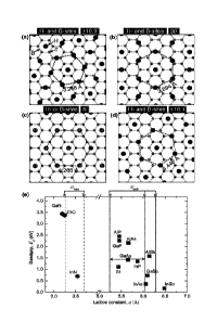
Figures la-ld show four different hexagonal structural configurations of the
semiconductor atoms in the (111) (or (0001)) planes of a semiconductor film on
top
of the hexagonal lattice of carbon atoms in the graphene layer, placed in such
a way
that no lattice mismatch will occur. As possible semiconductor adsorption
sites on
5 top of graphene, we consider 1) above the center of the hexagonal carbon
rings of
graphene (H-site) and 2) above the bridge between carbon atoms (B-site), as
indicated by arrows in figure la.
The figures show an idealised lattice-matched arrangement of the
semiconductor atoms in the (111) planes of a cubic crystal ((0001) planes for
10 hexagonal crystal) when the atoms are placed on 1) H- and B-sites
(figures la, lb
and 1d), and 2) H- or B-sites (figure lc). Dashed lines emphasize the
hexagonal
symmetry of the lattice of semiconductor atoms in the (111) plane. The
relative
rotations of these hexagons for each atomic arrangement are written on the top
of
each figure. For (figure la) and (figure 1d), two relative orientations are
possible,
10.9 and 16.1 , respectively (only the + rotations are shown in the images).
Figure 1 e shows artificial lattice-matched lattice constants for the atomic
arrangements in (a), (b) , (c) and (d). Dashed and solid lines correspond to
the
hexagonal (al) and cubic (a = al X -Ni 2) crystal phases of these lattices,
respectively.
The square (=) and the hexagon represent the cubic and the hexagonal phases,
respectively, for Si, ZnO, and binary III-v semiconductors.
If the semiconductor atoms are placed above alternating H- and B-sites as in
figure la, an exact lattice match can be achieved if the lattice constant, a,
of a cubic
semiconductor crystal (the lattice constant, a, is defined as the side length
of the
cubic unit cell) is equal to: 4.607 A. A few binary cubic semiconductors exist
with
lattice constants close to this value, with the closest being AN (a = 4.40 A)
and GaN
(a = 4.51 A). For hexagonal semiconductor crystals, exact lattice matches will
be
achieved if the lattice constant, al, is equal to: 3.258 A. A few binary
hexagonal
semiconductors exist with lattice constants close to this value, with the
closest being
SiC (al = 3.07 A), AN (al = 3.11 A), GaN (al = 3.19 A) and ZnO (al = 3.25 A)
crystals.
If the semiconductor atoms are placed above alternating H- and B-sites as in
figure lb, an exact lattice match can be achieved if the lattice constant, a,
of a cubic
CA 02916152 2015-12-18
WO 2014/202796 PCT/EP2014/063195
11
semiconductor crystal is equal to: 1.422 A x 3/2 x sqr(6) = 5.225 A. This is
close to
the lattice constant of GaP (a = 5.45 A), AlP (a = 5.45 A), InN (a = 4.98 A)
and ZnS
(a = 5.42 A). For hexagonal semiconductor crystals exact lattice matches will
be
achieved if the lattice constant, al, is equal to: 1.422 A x 3/2 x sqr(3) =
3.694 A.
This is close to the al lattice constants of the hexagonal forms of InN (al =
3.54 A)
and ZnS (al = 3.82 A) crystals.
For the atomic configuration as in figure lc, an exact lattice match can be
achieved if the lattice constant, a, of a cubic semiconductor crystal is equal
to: 1.422
A (carbon atom distance) x 3 x sqr(2) = 6.033 A. This is close to the lattice
constant
of group III-V compounds such as InAs, GaAs, InP, GaSb, AlSb and AlAs, and II-
VI compounds such as MgSe, ZnTe, CdSe, and ZnSe semiconductor crystals. In
particular, this is close to the lattice constant of group III-V compounds
such as InAs
(a = 6.058 A), GaSb (a = 6.096 A) and AlSb (a = 6.136 A), and II-VI compounds
such as ZnTe (a = 6.103 A) and CdSe (a = 6.052 A) semiconductor crystals.
For hexagonal semiconductor crystals, exact lattice matches will be achieved
if the lattice constant, al, is equal to: 1.422 A (carbon atom distance) x 3 =
4.266 A.
This is close to the al lattice constants of the hexagonal forms of the II-VI
materials
CdS (al = 4.160 A) and CdSe (al = 4.30 A) crystals which means that the
ternary
semiconductor CdSSe can provide a perfect lattice match for a certain molar
fraction
of S.
If the semiconductor atoms are placed above alternating H- and B-sites as in
figure ld, an exact lattice match can be achieved if the lattice constant, a,
of a cubic
semiconductor crystal is equal to: 6.28 A. This is close to the lattice
constant of InSb
(a = 6.479 A), MgTe (a = 6.42 A) and CdTe (a = 6.48 A).
Certain ternary compounds like e.g. InGaSb, InAsSb and AlInSb can provide
a perfect lattice match, as can some quaternary compounds like InGaAsSb and
AlInAsSb. For hexagonal semiconductor crystals, exact lattice matches will be
achieved if the lattice constant, al, is equal to: 4.44 A. This is close to
the al lattice
constants of the hexagonal forms of InSb (al = 4.58 A), MgTe (al = 4.54 A) and
CdTe (al = 4.58 A) crystals.
Without wishing to be limited by theory, due to the hexagonal symmetry of
the carbon atoms in graphitic layers, and the hexagonal symmetry of the atoms
of
CA 02916152 2015-12-18
WO 2014/202796 PCT/EP2014/063195
12
cubic or hexagonal semiconductors in the [111] and [0001] crystal direction,
respectively, a close lattice match between the graphitic substrate and
semiconductor
can be achieved when the semiconductor atoms are placed above the carbon atoms
of the graphitic substrate, ideally in a hexagonal pattern. This is a new and
surprising finding and can enable the epitaxial growth of films on graphitic
substrates.
The four different hexagonal arrangements of the semiconductor atoms as
described above, can enable semiconductor films of such materials to be grown.
Whilst it is ideal that there is no lattice mismatch between a growing film
and the substrate, small lattice mismatches are possible. The films of the
invention
ideally have a lattice mismatch of up to about 1% with the substrate. More
preferably, lattice mismatches should be 0.5% or less, e.g. 0.25% or less.
These
values apply to any film thickness. Lattice match values can be calculated
based on
a knowledge of the crystal structure of the semiconductor in question and the
information provided above. If a semiconductor can grow in a form with a
lattice
constant that matches any of the atomic arrangements depicted in figure la-ld
for its
(111) plane in case of cubic crystal or for its (0001) plane in case of
hexagonal
crystal, then an appropriate lattice match is present. For the avoidance of
doubt, the
lattice match should be calculated for the whole of the film present on the
substrate.
Note however, that the success of the process of the invention depends, to an
extent, on the thickness of the film. Thus, average strain for a total film
thickness of
100 nm should typically be less than 0.5%. Average strain for a total film
thickness
of 0.5 um should typically be less than 0.2%. Average strain for a total
thickness of
1 um should typically be less than 0.15%. Average strain for a total thickness
of 5
um should typically be less than 0.1%. In order to avoid defects in thicker
films
therefore, it is preferred if the lattice mismatch is as small as possible.
For some binary semiconductors like cubic InAs (a = 6.058 A), cubic GaSb
(a = 6.093 A), cubic CdSe (a = 6.052 A), and hexagonal CdSe (al= 4.30 A), the
lattice mismatch is so small (< ¨1%) that excellent growth of these binary
semiconductors can be expected for film thicknesses up to several tens of nm.
However, as the film grows thicker strain compensating growth techniques may
need to be employed in order to reduce the strain energy and avoid crystal
defects
CA 02916152 2015-12-18
WO 2014/202796 PCT/EP2014/063195
13
like dislocations. In essence therefore, film thickness up to the critical
thickness can
be achieved without defect risk. This will be of order 30 nm for 1.0% lattice
mismatch and of order 100 nm for 0.5% misfit. Thus, beyond the critical
thickness
superlattice techniques may be needed or different semiconductor materials
such as
ternary or quaternary semiconductors.
Of course, due to their nature, the lattice constants of ternary, quaternary
etc
compounds can be manipulated by changing the relative amount of each element
present. The lattice constants of these compounds can be tuned to a certain
value by
tuning the composition of these compounds. The use therefore, of ternary and
1 0 quaternary semiconductor compounds is preferred when thicker films,
such as more
than 100 nm, are desired. Devices may require a total film thickness of the
order of
5 um, typically from 1 to 10 um.
It is within the scope of the invention for the film being grown on the
substrate to comprise multiple layers of different group (III)(V) or (II)(VI)
compounds. Thus, a ternary or quaternary semiconductor might be grown on a
binary semiconductor.
Other multiple layer films might result from the use of compensating growth
techniques such as strained superlattices. If the film contains superlattices,
each
layer of the superlattice could have more than 1% strain if strain
compensation is
used such that the average lattice constant of the superlattice as a whole is
lattice-
matched to the graphitic substrate.
Such compensating growth techniques would be known to the skilled man.
It will be appreciated, however, that for certain semiconductor combinations
there might be too large mismatch between the lattice constant of the
semiconductor
and the lattice constant of graphene for successful film growth. In such
circumstances, it may not be possible to grow such a semiconductor directly
onto the
graphitic substrate.
Base Layer
In order to allow other semiconductor films to be present and maximise the
possibilities here, the inventors propose the use of an intermediate layer or
base
CA 02916152 2015-12-18
WO 2014/202796
PCT/EP2014/063195
14
layer between a semiconductor thin film and the substrate. This method is
preferably used where the semiconductor cannot be lattice matched with the
graphitic substrate or that the particular semiconductor for some reason does
not
form a thin film directly on the graphitic surface, e.g. because none of its
constituents have enough surfactant behaviour to cover the graphitic surface.
This intermediate layer is one which is lattice-matched and therefore forms a
kind of surfactant between a thin film semiconductor layer and the graphitic
substrate. The base layer material, which can be an element or compound has a
lattice mismatch of 2.5% or less, preferably 1% or less with graphene. For
example,
the lattice mismatch between (111) oriented Sb (rhombohedral A7) and graphene
is
1.0% when Sb atoms are positioned above H sites only, B sites only or T sites
only.
GaSb also has 1.0% lattice mismatch with graphene. InAs has 0.43% lattice
mismatch with graphene. This base layer need only be a few atomic layers
thick.
By using a base layer that itself is "3-dimensional", this layer provides lone
pairs through which a semiconductor layer can start to grow. The adhesion to
the
"2-dimensional" substrate is achieved via the use of the base layer.
The base layer is preferably a group V element or alloy of a group III-V
compound such as GaSb, InAs, AsSb, SbBi or Sb. AlSb might also be used. The
alloy As(0.077)-Sb(0.923) should be perfectly lattice-matched to graphene, in
the
configuration of Fig. 1(c). (Where 0.077 is the As molar fraction in the
alloy.)
Likewise an Sb-Bi alloy can be lattice-matched to the configuration in Fig. 1
(d).
Another option is a ternary lattice-matched base layer, such as those based
on AlAsSb, AlInSb, In GaSb or AlInAs. A further option is a combination of
base
layers, such as an elemental layer of Sb followed by a ternary layer as
described
above. The Sb layer could be as little as one atom thick although more likely
the
layer might be a two or three atoms thick.
A further option for the base layer might be CdSe or CdSSe. In one
embodiment CdSSe might be grown on a layer of CdSe to form the base layer.
The use of Sb is most preferred as the base layer. The (111)-oriented
bilayers of rhombohedral, A7, Sb has a close lattice match to graphene (1.0%
mismatch). The base layer can be deposited on the substrate using the
techniques
discussed in detail below in connection with the deposition of the
semiconductor.
CA 02916152 2015-12-18
WO 2014/202796 PCT/EP2014/063195
However, when the base layer is Sb, it is preferred if this is deposited under
mild conditions, such as less than 200 C, preferably 100 to 135 C, or such as
less
than 325 C, preferably 200 to 300 C, dependent on the flux intensity of Sb4 or
Sb2
that is used during deposition, the latter conditions being ideal for 5b2.
5 As noted above, only a few atomic layers (perhaps only one atomic
layer or
two atomic layers) of the base layer is required. In case of Sb, the minimum
would
be a (111)-oriented Sb bilayer. It should be considered that laying down one
Sb
atomic layer with the next layer being Ga is the same as a GaSb base layer and
hence the same as growing the GaSb directly on graphene. Once the base layer
is
1 0 present, the semiconductor film can be deposited. Where a base layer is
used, it may
be that the initial growth of semiconductor film takes place at a lower
temperature
similar as was used for the deposition of group V element (or group V alloy
etc). A
third step can then involve the deposition of III-V film(s) at higher
temperature
typical for normal epitaxial growth of the III-V compound in question. The
second
1 5 step above is preferred to avoid desorption of group V element (or
group V alloy)
during the third step.
It may be that to grow a superlattice on a graphitic substrate where each
layer
of the superlattice has too much strain for it to be possibly grown directly
on
graphene that a base layer is required, e.g. of Sb, GaSb or InAs. It may also
be
possible to use AlSb (lattice mismatch 1.7%).
The base layer may also be a "superlattice" with alternating atomic layers
[(111)-planes] of Sb and Bi. This superlattice would make a close lattice
match to
the "d" in Fig. 1(e) and thus provide a substrate with a lattice constant
where there
are no binary substrates available today.
Semiconductors
The semiconductor films of the invention are formed from at least one III-V
compound or at least one II-VI compound or a group IV compound such as SiC.
Group II elements are Be, Mg, Ca, Zn, Cd, and Hg. Preferred options here
are Zn and Cd.
CA 02916152 2015-12-18
WO 2014/202796 PCT/EP2014/063195
16
Group III options are B, Al, Ga, In, and Tl. Preferred options here are Ga, Al
and In.
Group V options are N, P, As, Sb. All are preferred.
Group VI options include 0, S, Se and Te. The use of 0, Se and Te is
preferred.
The manufacture of a group III-v film is preferred. It will be appreciated
that any compound which forms during film growth need not be completely
stoichiometric as the possibility of doping exists, as discussed below.
Preferred binary compounds for film manufacture include InAs, GaAs, AlAs,
InP, GaP, AlP, InSb, GaSb, AlSb, ZnTe, CdSe and ZnSe. It is within the scope
of
the invention to grow alternating thin layers (of order 1 nm or a few nm
thick) of
binary semiconductors such that the electronic properties and average lattice
constant of the thin film as a whole is matched with the substrate. The use of
GaSb
or InAs is highly preferred. Other options include ZnO and AlSb It is
preferred in
the film is not AN.
Whilst the use of binary materials is possible, the growth of ternary or
quaternary films or even quintinary films is preferred. Especially preferred
options
are InGaAs, InAlAs, InAsP, InPSb, InAsN, InPN, InSbN, GaInSb, GaAsN, GaInN,
GaPN, GaSbN, AlInSb,AlAsSb, AlSbP, AlInN, AlPN, AlAsN,AlSbN, InGaAsSb,
AlGaAsSb, and InGaAsN as these can be grown perfectly lattice-matched to
graphene, and are suitable for a number of devices. It will be appreciated
that in
ternary, quaternary etc materials the relative amounts of each ion can vary.
The ternary compounds may therefore be of formula XYZ wherein X is a
group III element, Y is a group III or V element different from X and Z and Z
is a
group V element. The X to Y or Y to Z molar ratio in XYZ is preferably 0.2 to
0.8,
i.e. the formula is preferably XxYl_xZ (or XY1,Zx) where subscript x is 0.2 to
0.8.
Quaternary systems may be represented by the formula AxBi_xCyDi_y where A and
B
are group III elements and C and D are group V elements. Again subscripts x
and y
are typically 0.2 to 0.8. Other options will be clear to the skilled man.
It is within the scope of the invention for the films to be doped. Doping
typically involves the introduction of impurity ions into the film. These can
be
introduced at a level of up to 1019/cm3, preferably up to 1018/cm3. The films
can be
CA 02916152 2015-12-18
WO 2014/202796 PCT/EP2014/063195
17
undoped, p-doped or n-doped as desired. Doped semiconductors are extrinsic
conductors whereas undoped ones are intrinsic.
Extrinsic semiconductors with a larger electron concentration than hole
concentration are known as n-type semiconductors. In n-type semiconductors,
electrons are the majority carriers and holes are the minority carriers. N-
type
semiconductors are created by doping an intrinsic semiconductor with donor
impurities. Suitable donors for III-V compounds can be e.g. Si and Te.
Suitable
donors for group IV semiconductors can be e.g. P and As.
The p-type semiconductors have a larger hole concentration than electron
concentration. The phrase 'p-type' refers to the positive charge of the hole.
In p-type
semiconductors, holes are the majority carriers and electrons are the minority
carriers. P-type semiconductors are created by doping an intrinsic
semiconductor
with acceptor impurities. Suitable acceptors for III-V compounds can be e.g.
Be and
Zn. Suitable acceptors for group IV semiconductors can be e.g. B. It will be
appreciated that whether an impurity will act as a donor or acceptor in a III-
V
compound will in some cases depend on the orientation of the growing surface
and
the growth conditions. Dopants can be introduced during the growth process or
by
ion implantation of the films after their formation. Doping may also be
effected by
allowing impurities from the substrate to enter the semi-conductor film.
Preferred films of the invention will contain dopants.
Once the film growth has been established on the graphene substrate, there is
no real limit to the manipulations that can be carried out. Different film
layers can
be added simply by changing the nature of the atoms present. For example, a
film is
established, it would also be possible to grow a top film layer in which there
was a
"p-i-n" or "n-i-p" structure by use of appropriate doping techniques. Thus,
initially
the film might be p-doped before an undoped intrinsic layer is applied and an
n-
doped layer is introduced (or vice versa).
It will be appreciated that doping only part/parts of the film is possible,
e.g.
using ion implantation for specific components. Doping may therefore occur
processing after growth.
Films
CA 02916152 2015-12-18
WO 2014/202796 PCT/EP2014/063195
18
The films grown in the present invention may be from 250 nm to several
microns in thickness, e.g. 0.5 to 10 microns, more preferably 1 to 5 microns.
The
surface area of the films is limited only by the apparatus used to deposit the
films
and the size of the substrate. The surface area may also be dictated by the
size of the
holes in which the film is grown, as described further below.
The thickness of the films is often controlled by the length of time for which
the growing process runs. A longer process typically leads to a thicker film.
The base layer when present may be one or two atomic thicknesses, e.g. 2 A
or more up to 10's of nanometres depending on the nature of the base layer and
the
nature of the thin film grown upon that base layer.
Film/Base layer deposition/growth
We deal firstly with the direct deposition of films of the invention on a
graphitic substrate. The films of the invention grow epitaxially on the
substrate or
base layer. They attach to the underlying graphitic substrate through
covalent, ionic
or quasi van der Waals binding. Accordingly, at the junction of the substrate
and the
film, crystal planes are formed epitaxially. These build up, one upon another,
in the
same crystallographic direction thus allowing the epitaxial growth of the
film.
The films of the invention should preferably grow in the [111] direction for
films with cubic crystal structure and [0001] direction for films with
hexagonal
crystal structure. Planes (111) and (0001) both represent the same (hexagonal)
plane
of the film, it is just that the nomenclature of the plane varies depending on
the
crystal structure of the growing film.
The films are preferably grown by molecular beam epitaxy (MBE). Whilst it
is within the scope of the invention for vapour deposition to be used, e.g. a
CVD
especially a metal organic CVD (MOCVD) or metal organic vapour phase epitaxy
(MOVPE) method, the use of MBE is highly preferred.
In this method, the substrate is provided with a molecular beam of each
reactant, e.g. a group III element and a group V element preferably supplied
simultaneously. It may, however, be advantageous to begin the deposition
process
CA 02916152 2015-12-18
WO 2014/202796 PCT/EP2014/063195
19
using one reactant at a time. Thus a first layer might involve deposition of
Sb
followed by the application of Ga. A first layer might involve deposition of
In
followed by As or vice versa. The deposition might involve growth of AlSb,
preferably Sb then Al. Once both reactants are present and each has formed an
atomic layer, a compound of these two will form. This alternating deposition
may or
may not be repeated one or more times. Thereafter, both ions can be supplied
simultaneously and a film will continue to grow. The substrate temperature may
need to be raised before growing in conventional MBE mode with group III-V
elements.
A higher degree of control of the nucleation and growth of the films on the
graphitic substrate might be achieved with the MBE technique by using
migration-
enhanced epitaxy (MEE) where group (III) (V) elements are supplied alternately
with no time in between or atomic-layer MBE (ALMBE) where e.g. the group III
and V elements can be supplied alternately with a delay in between.
A preferred technique is solid-source MBE, in which very pure elements
such as gallium and antimony are heated in separate effusion cells, until they
begin
to slowly evaporate (e.g. gallium) or sublimate (e.g. antimony). The gaseous
elements then condense on the substrate, where they may react with each other.
In
the example of gallium and antimony, single-crystal gallium antimonide is
formed.
The use of the term "beam" implies that evaporated atoms (e.g. gallium) or
molecules (e.g. 5b4 or 5b2) do not interact with each other or vacuum chamber
gases
until they reach the substrate.
Doping ions can also be introduced easily using MBE. Figure 2 is a possible
set up of an MBE process.
Molecular beam epitaxy (MBE) takes place in ultra high vacuum, with a
background pressure of typically around 10-10 to 10-9 Torr. Films are
typically
grown slowly, such as at a speed of up to a few, such as about 2, pm per hour.
This
allows films to grow epitaxially and maximises structural performance.
The growth temperature may be in the range 300 to 700 C for a conventional
II-VI or III-V semiconductor film. Much lower temperatures are needed for base
layer growth which is typically around 130 C. The temperature employed is,
however, specific to the nature of the material in the film, the surface
orientation,
CA 02916152 2015-12-18
WO 2014/202796 PCT/EP2014/063195
and fluxes of III and V elements used. For GaAs growth on GaAs(001) surface, a
preferred temperature is 580 to 630 C, e.g. 590 C. For GaAs growth on
GaAs(111)
surface, such as the GaAs(111)B surface a higher temperature is preferred,
e.g.
530 C or higher such as 610 C or higher. For InAs and GaSb the range is lower,
for
5 example 430 to 540 C, such as 450 C for InAs growth on InAs (001) surface
and
465 C for GaSb growth on GaSb(111) surface. GaSb growth on GaSb(001) surface
may occur at 490 C. Appropriate temperatures will be found by the skilled
person.
Film growth can be initiated by opening the shutter of the Ga/In effusion cell
and the shutter and/or valve of counter ion effusion cell (e.g. arsenic or
antimony),
10 simultaneously (continuous (analog or digital) MBE growth) or
alternating (MEE,
ALMBE).
The temperature of the effusion cells can be used to control growth rate.
Convenient growth rates are 0.05 to 2 pm per hour, e.g. 1 pm per hour.
The beam equivalent pressure (flux) of the molecular beams can also be
1 5 adjusted depending on the nature of the film being grown. Suitable
levels for beam
equivalent pressures are between 1 x 10⁻⁸ and 1 x 10⁻⁵ Torr.
The beam flux ratio between reactants (e.g. group III atoms and group V
molecules) can be varied, the preferred flux ratio being dependent on other
growth
parameters and on the nature of the film being grown.
20 A significant benefit of MBE is that the growing film can be analysed
in situ,
for instance by using reflection high-energy electron diffraction (RHEED).
RHEED
is a technique typically used to characterize the surface of crystalline
materials. This
technology cannot be applied so readily where films are formed by other
techniques
such as MOVPE.
As noted above, the films of the invention preferably grow as cubic (zinc
blende) or hexagonal (wurtzite) structures. It is also within the scope of the
invention for the nature of the material forming the film to be changed during
the
growing process. Thus, by changing the nature of the molecular beams, a
portion of
different structure would be introduced into a film. An initial GaAs film
could be
extended with an InAs film section for example by changing from a Ga feed to
an In
feed. The GaAs/InAs film could then be extended with a GaAs film section by
changing back to a Ga feed and so on. It is also within the scope of the
invention to
CA 02916152 2015-12-18
WO 2014/202796
PCT/EP2014/063195
21
include nanostructures in the film during the growing process, e.g. InAs or
GaSb
quantum dots in GaAs matrix. The growth of such nanostructures will be known
to
the skilled man. Again, by developing different structures with differing
electrical
properties, the inventors offer films with interesting and manipulable
electronic
properties which can be tailored by the manufacturer towards all manner of end
applications.
Where a base layer is present, the base layer is preferably deposited using
one of the techniques described above, e.g. ALMBE. Thereafter, semi-conductor
formation follows the instructions above.
1 0 In one embodiment, after an initial elemental base layer film is
deposited,
often an Sb layer, a second elemental layer, typically of a different material
can be
deposited such as a Ga layer. It may be worthwhile to lay down alternate
atomic
layers such as of Sb and Ga before starting to grow a desired semiconductor
but
preferably only one atomic layer of Ga is laid down and this marks the start
of the
1 5 GaSb layer, on top of which e.g. InAs or a ternary or a quaternary
compounds could
be grown.
It may also be useful, initially to apply a flux of the components of the semi-
conductor separately. Thus a flux of element (III) is applied and then element
(V),
or alternatively in the reverse order, before a joint simultaneous flux can be
used to
20 grow the film.
If a base layer is used which is heat sensitive, such as an Sb base layer,
once
III-V film growth is established, temperature can be increased to conventional
epitaxial deposit temperatures. The semiconductor film grown need not be the
same
as the base layer or contain the element(s) of the base layer.
25 The base layer or main film can be doped. Once semiconductor film
growth
has started doping can be initiated. If present, doping should be begun a few
atomic
layers into film formation. This will ideally introduce an ohmic contact into
the
film. A preferred dopant is Si or Te. Alternatively, the dopant can be Be, or
Mg.
Mg is used as a preferred dopant for p-type nitrides. Be is used as preferred
dopant
30 for p-type arsenides and antimonides. Si is used as preferred dopant for
n-type
arsenides and nitrides, whereas Te is used as preferred dopant for n-type
antimonides.
CA 02916152 2015-12-18
WO 2014/202796 PCT/EP2014/063195
22
It will be appreciated that doping only part/parts of the film is possible,
e.g.
using ion implantation for specific components. Doping may therefore occur
processing after growth.
In one embodiment, the film can be grown on a substrate provided with a
mask. The mask protects the substrate but defines a pattern of holes in which
film
growth is intended. For example, a silicon dioxide or alumina mask can be
applied
on a graphitic substrate with a pattern of holes in the mask through which
film
growth occurs. Once film deposition has taken place, the mask can be left in
place,
partially removed or completely removed, e.g. by etching, to leave a series of
thin
films on the substrate corresponding to the position of the holes in the mask.
Applications
The films of the invention have wide ranging utility. They are semi-
1 5 conductors so can be expected to offer applications in any field where
semiconductor technology is useful. They are primarily of use in electronics
and
optoelectronic applications, e.g. in solar cells, photodetectors, light-
emitting diodes
(LEDs), waveguides and lasers.
An ideal device for their deployment might be a thin film solar cell. Such
solar cell has the potential to be efficient, cheap and lightweight at the
same time.
This is a rapidly developing field and further applications on these valuable
materials will be found in the next years.
The invention will now be further discussed in relation to the following non
limiting examples and figures.
Brief Description of the Figures
Figure la-d shows the atomic arrangements when semiconductor atoms are
placed above 1) H- and B- sites (Figure la, b, and d), and 2) H- or B-sites
(Figure
lc) on graphene. In Figure le the bandgap energies of the III-V semiconductors
(as
well as Si and ZnO) are plotted against their lattice constants. Vertical
solid (dashed)
coloured lines depict the lattice constant of an ideal crystal that would give
perfect
CA 02916152 2015-12-18
WO 2014/202796 PCT/EP2014/063195
23
lattice match with graphene for a cubic (hexagonal) crystal with the four
different
atomic arrangements (Figure la-d) with respect to graphene. In the case of
some
binary semiconductors, the lattice mismatch with graphene is very small (e.g.
InAs,
GaSb, and ZnO) for one suggested atomic configuration. For other binary
semiconductors like GaAs, the lattice mismatch is quite large and in-between
two
different atomic configurations (as in Figure lb or Figure lc). It can be
realized
from the figure that many ternary, quaternary and quintinary semiconductors
can be
perfectly lattice-matched to graphene.
Figure 2 shows an MBE experimental set up.
Figure 3 is a theoretical side view of a support, graphene layer, base layer
and top semiconductive layer.
Figure 4 shows a thin film of GaSb grown directly on a Kish graphite
surface.
Figure 5 shows that for SbGp13, triangle-like shaped GaSb platelets confirm
the epitaxial relation with graphite substrate.
Experimental procedure:
Thin film is grown in a Varian Gen II Modular molecular beam epitaxy
(MBE) system equipped with a regular Al filament cell, a Ga dual filament
cell, an
In SUMO dual filament cell, an As valved cracker cell, and an Sb valved
cracker
cell allowing to fix the proportion of dimers and tetramers. In the present
study, the
major species of arsenic are As2, and antimony are 5b2.
Growth of thin film is performed either on a Kish graphite flake or on a
graphene film (1 to 7 monolayers thick, preferably only one monolayer thick)
grown
either by a chemical vapor deposition (CVD) technique directly on a metal film
such
as Cu, Ni, and Pt, or grown on SiC substrates by using a high-temperature
sublimation technique. The graphene film samples are purchased from external
suppliers. The CVD graphene films are purchased from "Graphene Supermarket",
USA.
The CVD graphene film samples are cleaned by isopropanol followed by a
blow dry with nitrogen, and then indium-bonded to a silicon wafer. The
CA 02916152 2015-12-18
WO 2014/202796 PCT/EP2014/063195
24
graphene/SiC substrates are blow dried with nitrogen, and then indium-bonded
to a
silicon wafer.
The samples are then loaded into the MBE system for the thin film growth.
The samples are annealed at a substrate temperature of 550 C (or higher) for
a
duration of 10 minutes to get rid of any oxide residues on the substrate. The
deposition of III-V film is typically done by a three-step (if a base layer is
used) or a
two-step growth method. In case a base layer is used, the first step involves
the
deposition of a group V element (or of an alloy of group V elements) on the
graphitic layers at lower substrate temperatures as described below. The
second step
involves the growth of III-V film at a lower substrate temperature similar as
was
used for the deposition of group V element (or group V alloy). The third step
involves the deposition of III-V film(s) at higher temperature typical for
normal
epitaxial growth of the III-V compound in question. The second step above is
preferred to avoid desorption of group V element (or group V alloy) during the
third
step.
Example 1:
After annealing the graphene substrate at 550 C, the substrate temperature is
then decreased to typically between 200 C and 300 C for Sb deposition. Sb
flux is
first supplied to the surface during a time interval typically in the range 5
s to 1
minute, dependent on Sb flux and substrate temperature. A few nm, preferably
less
than a few tens of nm, of Sb are then grown, preferably by MEE or ALMBE. Then,
the substrate temperature is increased to a temperature suitable for GaSb thin
film
growth: i.e. around 450 C. The temperature of the Ga effusion cell is preset
to yield
a nominal planar growth rate of 0.3 [inn per hour. The 5b2 flux is set to 1x10-
6 Torr
to grow the GaSb thin film at this temperature. The GaSb thin film is doped to
a
level appropriate for which device structure will be grown on top of this thin
film
template structure.
Example 2:
CA 02916152 2015-12-18
WO 2014/202796 PCT/EP2014/063195
After annealing the graphene substrate at 550 C, the substrate temperature is
decreased to between 15 C and 80 C for As deposition, the temperature being
dependent on which deposition rate is wanted. As flux is first supplied to the
surface
during a time interval typically in the range 5 s to 1 minute. A few nm,
preferably
5 less than a few tens of nm, InAs are then grown, preferably by MEE or
ALMBE.
Then, the substrate temperature is increased to a temperature suitable for
InAs thin
film growth: i.e. around 450 C. The temperature of the In effusion cell is
preset to
yield a nominal planar growth rate of up to 0.7 [tm per hour. The As2 flux is
set to
6x10⁻⁶ Torr to form the InAs thin film at this temperature. The InAs thin film
is
10 doped to a level appropriate for which device structure will be grown on
top of this
thin film template structure.
The substrates prepared in examples 1 and 2 hereby called as III-V/GP thin
film substrate can be used as a template for the fabrication of various
optoelectronic
or electronic devices, and solar cells.
15 In Examples 3-4 below, we describe the deposition of 1) p-i-n doped
homojunction GaSb thin film on III-V/GP thin film substrate, and 2) p-n doped
heterostructure GaSb/InGaAsSb thin film on III-V/ GP thin film substrate.
These
thin film structures are intended to use for applications such as light
emitting diodes
and photo detectors.
Example 3:
p-i-n doped homojunction GaSb thin film is further grown on III-V/GP thin
film substrate of example 1 to use it as a photodetector. The thickness of
each of the
p-doped, n-doped, and intrinsic III-V epilayer is typically kept between 0.5
and 3
gm. For p-type doping, Be is used. Te is used as an n-dopant. The Be cell
temperature is set to 990 C which gives a nominal p-type doping concentration
of 3
x 1018cm-3. The Te cell temperature is set to 440 C which gives a nominal n-
type
doping concentration of 1 x 1018 cm-3. The deposition temperature for all the
layers
is set to 450 C. The temperature of the Ga effusion cell is preset to yield a
nominal
planar growth rate of 0.7 [tm per hour, and the 5b2 flux is set to 1x10⁻⁶ Torr
to grow
the GaSb thin film.
CA 02916152 2015-12-18
WO 2014/202796 PCT/EP2014/063195
26
Example 4:
p-type GaSb / intrinsic GaInAsSb / n-type GaSb thin film is further grown
on III-V/GP thin film substrate. The composition of the intrinsic GaInAsSb is
tailored such that it is lattice-matched to GaSb. The thickness of each these
three
epilayers is typically kept between 0.5 and 3 gm. For p-type doping, Be is
used. Te
is used as an n-dopant for the GaInAsSb epilayer. The Be cell temperature is
set to
990 C which gives a nominal p-type doping concentration of 3 x 1018cm-3. The
Te
cell temperature is set to 440 C which gives a nominal n-type doping
concentration
of 1 x 1018 cm-3.
Example 5:
n-type GaSb / n+ GaInAsSb / p-GaInAsSb /p+ GaInAsSb thin film is
further grown on III-V/GP thin film substrate to use it as a photodetector.
The
composition of the GaInAsSb is tailored such that it is lattice-matched to
GaSb. The
thickness of each of these epilayers is typically kept between 0.5 and 3 gm.
For p-type doping, Be is used. Te is used as an n-dopant for the GaInAsSb
epilayer.
The Be cell temperature is set to 990 C which gives a nominal p+ type doping
concentration of 1 x 1018cm-3, and the Be cell temperature is set to 940 C
which
gives a nominal p-type doping concentration of 9 x 1016cm-3 The Te cell
temperature is set to 440 C which gives a nominal n-type doping concentration
of 1
x 1018 cm-3.
Example 6:
A series of thin films were grown directly on a Kish graphite. The
conditions of growth are summarised in table 1. After annealing the sample at
550
C, the substrate temperature is reduced to the temperature shown in column
2which the thin film is grown. The SEM images in figure 4 show that we have
grown GaSb crystal material on Kish graphite.
CA 02916152 2015-12-18
WO 2014/202796 PCT/EP2014/063195
27
Nucleation: Samples SbGp13, SbGp 22 and SbGp 17 show that GaSb
nucleates on Kish graphite and forms triangle-like shaped GaSb platelets due
to
epitaxial relation with the graphitic surface. Nucleation can be achieved with
regular MBE at 300 C and with MEE (Migration-Enhanced Epitaxy method in
MBE) at 200 C and at 300 C. The material deposited on the Kish graphite is the
equivalent of 3 monolayers (ML) of GaSb in each case.
Thin film: Samples SbGp24/26/27/31 show that an almost continuous film of
GaSb with nominal thickness 100 nm can be grown on Kish graphite using a two-
step growth method (MEE nucleation step at 300 C + MBE growth at 300-520 C).
The samples SbGp26/27/31 are grown according to such two-step method
(MEE step at low temp + MBE step at higher temp), i.e. Sb base layer was not
used
for these samples.
- 28 -
0
i Sample I
Number Growth details
Short description of the sample
SbGp 13 GaSb thin film: 5 sec (3 ML), Sb flux=lx10^-6, Ga=0.7MLs-1,
Tc=300 C. 3 ML GaSb dep at Tc=300C
Sb flux predep= lx10^-6, 5 min at Tc=400 C.
SbGp 14 GaSb thin film: 5 sec (3 ML), Sb flux=lx10^-6, Ga=0.7MLs-1,
Tc=300 C.
GaSb thin film: MEE 5 sec (3 ML), Sb flux=lx10^-6, Ga=0.7MLs-1, Tc=300
=SbGp 15 C.
[Open Sb 1.4 sec + Open Ga 1.4 sec + wait 2]x3 times 3 ML MEE GaSb dep at
Tc=300C
cio
SbGp 16 GaSb thin film: 5 sec (3 ML), Sb flux=1x10^-6, Ga=0.7MLs-1,
Tc=350 C. 3 ML GaSb dep at Tc=350C
=
GaSb thin film: MEE 5 sec (3 ML), Sb flux=lx10^-6, Ga=0.3MLs-1, 3 ML MEE
GaSb dep at Tc=300C, Ga=0.3
SbGp 17 Tc=300 C. [Open Sb 3.4 sec + Open Ga 3.4 sec + wait 2]x3 times
MLs-1
GaSb thin film: MEE 5 sec (3 ML), Sb flux=6x10^-7, Ga=0.3MLs-1, 3
ML MEE GaSb dep at Tc=300C, Ga=0.3
SbGp 18 Tc=300 C. [Open Sb 3.4 sec + Open Ga 3.4 sec + wait 2]x3 times
MLs-1, LOW Sb flux
=
GaSb thin film: MEE 5 sec (3 ML), Sb flux=1.5x10^-6, Ga=0.3MLs-1, 3 ML MEE
GaSb dep at Tc=300C, Ga=0.3 1-d
SbGp 19 Tc=300 C. [Open Sb 3.4 sec + Open Ga 3.4 sec + wait 2]x3 times
MLs-1, High Sb flux
1-d
GaSb thin film: Two temp MEE, Sb flux=lx10^-6, Ga=0.3MLs-1, Tc=300 C.= Two
temp MEE: 1 ML at 300C and 2 MLs
SbGp 20 [Open Sb 1.7 sec + Open Ga 1.7 sec + wait 2]x2 times + Tc=400 C.
[Open = at 400C
- 29 -
0
i Sample
Number Growth details
Short description of the sample
Sb 3.4 sec + Open Ga 3.4 sec + wait 2]x2 times
GaSb thin film: Two temp MEE, Sb flux=lx10^-6, Ga=0.3MLs-1, Tc=300 C.
[Open Sb 1.7 sec + Open Ga 1.7 sec + wait 2]x2 times + Tc=375 C. [Open Two
temp MEE: 1 ML at 300C and 2 MLs
SbGp 21 Sb 3.4 sec + Open Ga 3.4 sec + wait 2]x2 times at
375C
GaSb thin film: MEE 5 sec (3 ML), Sb flux=lx10^-6, Ga=0.3MLs-1, 3
ML MEE GaSb dep at Tc=200C, Ga=0.3
SbGp 22 Tc=200 C. [Open Sb 3.4 sec + Open Ga 3.4 sec + wait 2]x3 times
MLs-1
GaSb thin film: MEE 5 sec (3 ML), Sb flux=lx10^-6, Ga=0.3MLs-1, 3
ML MEE GaSb dep at Tc=325C, Ga=0.3
SbGp 23 Tc=325 C. [Open Sb 3.4 sec + Open Ga 3.4 sec + wait 2]x3 times
MLs-1
GaSb thin film: 100 nm thick, Sb flux=lx10^-6, Ga=0.3MLs-1, Tc=300 C. 100
nm GaSb dep at Tc=300C, Ga=0.3
SbGp 24 [Open Sb 3.4 sec + Open Ga 3.4 sec + wait 2]x20 times + GaSb 980
sec. MLs-1
GaSb thin film: MEE 5 sec (3 ML), Sb flux=8x10^-7, Ga=0.1MLs-1, = 3
ML MEE GaSb dep at Tc=300C, Ga=0.1
SbGp 25 = Tc=300 C. [Open Sb 3.4 sec + Open Ga 3.4 sec + wait 2]x9 times
MLs-1 1-d
GaSb thin film: 100 nm thick, Sb flux=lx10^-6, Ga=0.3MLs-1, Tc=300 C. =
1-d
=
[Open Sb 3.4 sec + Open Ga 3.4 sec + wait 2]x30 times + GaSb 980 sec at = 100
nm GaSb dep: 3 nm at Tc=300C, 98
SbGp 26 Tc=450C. nm
at Tc=450C
- 30 -
0
i Sample
Number Growth details
Short description of the sample
GaSb thin film: 100 nm thick, Sb flux=lx10^-6, Ga=0.3MLs-1, Tc=300 C.
[Open Sb 3.4 sec + Open Ga 3.4 sec + wait 2]x30 times + 100 sec at 100
nm GaSb dep: 3 nm MEE + 10 nm at
SbGp 27 Tc=300C+ GaSb 800 sec at Tc=450 C.
Tc=300C, 80 nm at Tc=450C
GaSb Te thin film: MEE 5 sec (3 ML), Sb flux=lx10^-6, Ga=0.3MLs-1,
GaTe=600C, Tc=300 C. [Open Sb 3.4 sec + Open Ga and GaTe 3.4 sec +
p
SbGp 28 wait 2]x3 times
o
=
GaSb Te thin film: MEE 5 sec (3 ML), Sb flux=lx10^-6, Ga=0.3MLs-1,
= GaTe=550C, Tc=300 C. [Open Sb 3.4 sec + Open Ga and GaTe 3.4 sec +
SbGp 29 wait 2]x3 times