Note: Descriptions are shown in the official language in which they were submitted.
CA 02916569 2015-12-22
WO 2014/209739
PCT/US2014/043137
POWER CABLE TERMINAL CONNECTION DEVICE
TECHNICAL FIELD
[0001] The invention relates to terminal connections for power cables.
BACKGROUND
[0002] As electrical power distribution becomes more complex through the
advent of renewable energy,
distributed generation and the adoption of electric vehicles, intelligent
electrical distribution and
associated electrical sensing is becoming more useful and even necessary.
Useful sensing may include
voltage, current, and the time relationship between voltage and current at
various locations within a power
distribution network.
[0003] In addition, during replacement of an existing cable termination, e.g.,
for repair/maintenance or
feature upgrades, such as adding sensing capabilities, reconnecting the
existing cable to the new
termination can be a difficult operation. For example, replacing a cable
termination may include cutting
off the existing cable termination in its installed location. Such installed
locations may include switchgear
enclosures, bus bar cabinets, or adjacent generators, motors, transformers, or
other equipment. The
installed locations may provide limited space to perform the replacement and
to fit the replacement
termination. In addition, when an existing cable termination is removed, the
remaining power cable may
be shortened somewhat. This shortening of the cable may cause additional
difficulties because the
shortened cable will still need to provide an electrical connection to its
original endpoint.
SUMMARY
[0004] In general, this disclosure is directed to terminal connections for
power cables, such as medium
and high voltage power cables. This disclosure includes techniques for
replacing a terminal connection in
an existing cable installation as well as terminal connections suitable for an
initial installation. In some
examples, this disclosure is directed to terminal connections providing
sensing capabilities, such as
voltage and/or current sensing capabilities. The sensing capabilities may be
provided by retrofitting an
existing cable installation with new terminal connection components, such as a
new complete terminal
connection or a new terminal connection adapter.
[0005] In one aspect, the disclosure is directed to a terminal connection
device that comprises a
contiguous body disposed onto an inner conductor. The inner conductor includes
a first end mateable
with a power cable connector and a second end. The body comprises a multilayer
structure having an
inner conductive or semiconductive layer disposed over at least a portion of
the power cable connector, an
insulating layer and an outer conductive or semiconductive layer. The body
surrounds the first end of the
inner conductor and extending towards the second end of the inner conductor.
The body also includes an
electrically isolated section of conductive or semiconductive material.
1
CA 02916569 2015-12-22
WO 2014/209739
PCT/US2014/043137
[0006] In another aspect, an assembly comprises the terminal connection device
described above,
wherein the body covers a power connector and an end portion of a power cable.
[0007] In another aspect, an adapter for providing a connection between a
power cable and a connection
interface comprises a contiguous body overmolded onto an inner conductor. The
inner conductor
includes a first end mateable with a power cable connector and a second end
mateable with a connection
interface. The body comprises a multilayer structure having an inner
conductive or semiconductive layer
disposed over at least a portion of the power cable connector, an insulating
layer and an outer conductive
or semiconductive layer. The body surrounds the first end of the inner
conductor and extending towards
the second end of the inner conductor, wherein the second end of the inner
conductor extends beyond an
end of the body.
[0008] In another aspect, a terminal connection device comprises an inner
conductor and a contiguous
body disposed onto the inner conductor. The contiguous body comprises an
insulating layer surrounding
the inner conductor and extending beyond a first end of the inner conductor to
form a hollow interior
section adjacent to the end of the inner conductor. The body also includes an
outer conductive or
semiconductive layer adjacent to and surrounding the insulating layer. The
body also includes an
electrically isolated section of conductive or semiconductive material in
contact with an outer surface of
the insulating layer. The terminal connection device is configured to receive
an end of a cable conductor
of the power cable such that the end of cable conductor of the power cable
fits within the hollow interior
section and electrically connects to the first end of the inner conductor. The
electrically isolated section
of conductive or semiconductive material forms an electrode of a sensing
capacitor of a capacitive voltage
sensor. The insulating layer is operable to form a dielectric of the sensing
capacitor of the capacitive
voltage sensor.
[0009] In another aspect, an assembly includes the terminal connection device
and a power cable. The
power cable includes a cable conductor extending along a length of the power
cable, a cable insulating
layer surrounding the cable conductor except a portion of the cable conductor
that protrudes from the
cable insulating layer at an end portion of the power cable, an inner cable
semiconductor or conductor
layer between the cable conductor and the cable insulating layer, the inner
cable semiconductor or
conductor layer being adjacent to the cable insulating layer, and an outer
cable semiconductor or
conductor layer adjacent to and surrounding the cable insulating layer.
[0010] In a further aspect, an adapter comprises an inner conductor having a
first end and a second end
and a contiguous body disposed onto the inner conductor. The body comprises an
insulating layer
surrounding the inner conductor and extending beyond the first end of the
inner conductor to form a
hollow interior section adjacent to the first end of the inner conductor. The
body also comprises an outer
conductive or semiconductive layer adjacent to and surrounding the insulating
layer. The body also
comprises an electrically isolated section of conductive or semiconductive
material in contact with an
outer surface of the insulating layer. The adapter is configured to receive an
end of a cable conductor of a
2
CA 02916569 2015-12-22
WO 2014/209739
PCT/US2014/043137
power cable such that the end of the cable conductor of the power cable fits
within the hollow interior
section and electrically connects to the first end of the inner conductor. The
second end of the inner
conductor extends beyond the insulating layer and the outer conductive or
semiconductive layer, wherein
the second end of the inner conductor opposes the first end of the inner
conductor, and wherein the
second end of the inner conductor is mateable with a connection interface.
[0011] In another aspect, a method for retrofitting a power cable comprises
disconnecting a cable
accessory from the power cable, mating a first end of an adapter, such as
described herein, to an end of
the power cable, and mating a second end of the adapter to a connection
interface.
[0012] In another aspect, a method for installing a terminal connection device
with a capacitor on a
power cable to facilitate voltage sensing comprises attaching a power cable
connector onto an end of the
power cable. A terminal connection device, including the capacitor, is mated
to the power cable
connector on the end of the power cable. The terminal connection device
comprises the terminal
connection device described herein.
[0013] In another aspect, a method for retrofitting a power cable comprises,
disconnecting a cable
accessory from the power cable and mating a terminal connection device
including the capacitor, such as
described herein, to an end of the cable.
[0014] The above summary of the present invention is not intended to describe
each illustrated
embodiment or every implementation of the present invention. The details of
one or more examples of
this disclosure are set forth in the accompanying drawings and the description
below. Other features,
objects, and advantages of the disclosed techniques will be apparent from the
description and drawings,
and from the claims.
BRIEF DESCRIPTION OF DRAWINGS
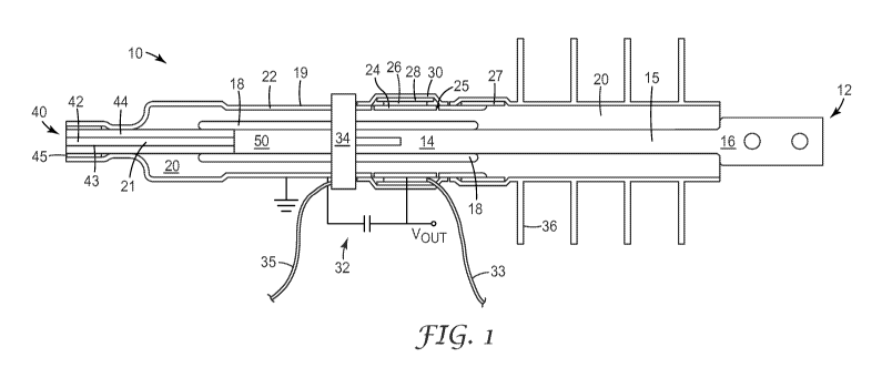
[0015] FIG. 1 is an illustration of an example terminal connection device that
includes an electrically
isolated section of conductive or semiconductive material forming an electrode
of a sensing capacitor of a
capacitive voltage sensor.
[0016] FIG. 2 is an illustration of an example terminal connection device that
includes a T body and an
electrically isolated section of conductive or semiconductive material forming
an electrode of a sensing
capacitor of a capacitive voltage sensor.
[0017] FIGS. 3A¨ 3D illustrate example steps for installing the terminal
connection device of FIG. 2 on
a power cable.
[0018] FIG. 4A is an illustration of a terminal connection device that
includes an adapter with an
electrically isolated section of conductive or semiconductive material forming
an electrode of a sensing
capacitor of a capacitive voltage sensor.
3
CA 02916569 2015-12-22
WO 2014/209739
PCT/US2014/043137
[0019] FIG. 4B is an illustration of a terminal connection device that
includes an adapter with an
electrically isolated section of conductive or semiconductive material forming
an electrode of a sensing
capacitor of a capacitive voltage sensor.
[0020] FIG 5 is a flowchart illustrating steps for retrofitting a power cable
with a terminal connection
device or an adapter including a capacitive voltage sensor.
[0021] FIG 6 is an illustration of an assembly including the adapter of FIG 4
installed on various
terminal connections including an elbow.
DETAILED DESCRIPTION
[0022] In the following Detailed Description, reference is made to the
accompanying drawings, which
form a part hereof, and in which is shown by way of illustration specific
embodiments in which the
invention may be practiced. In this regard, directional terminology, such as
"top," "bottom," "front,"
"back," "leading," "forward," "trailing," etc., is used with reference to the
orientation of the Figure(s)
being described. Because components of embodiments of the present invention
can be positioned in a
number of different orientations, the directional terminology is used for
purposes of illustration and is in
no way limiting. It is to be understood that other embodiments may be utilized
and structural or logical
changes may be made without departing from the scope of the present invention.
The following detailed
description, therefore, is not to be taken in a limiting sense, and the scope
of the present invention is
defined by the appended claims.
[0023] The present disclosure describes a terminal connection device for use
in medium or high voltage
power connection applications. In many aspects, the terminal connection device
includes integrated
sensor technology. The terminal connection device can be a fully integrated
structure, such as shown in
Figs. 1 ¨ 2, having a pre-installed connection interface. Alternatively, the
terminal connection device
can be configured as an adapter which can be mounted in the field to a
connection interface. In either
aspect, the terminal connection device is retrofittable, in that it can be
used to replace existing cable
accessories with a new accessory having integrated sensing technology.
Further, the terminal connection
device described herein can directly connect an existing power utility cable
to a connection interface
without the need for using an interface cable. In addition, components of the
incorporated capacitive
voltage sensor can be factory-molded to specific dimensions, allowing for
precise and direct measurement
of the voltage of a conductor, while reducing or eliminating calibration time
and cost. Further, the
terminal connection device can be dimensionally smaller than conventional
field-assembled solutions that
include an interface cable. The terminal connection device can be particularly
useful in tight spaces such
as in switchgears, generators, transformer boxes, busbar installations, and
motors. In some embodiments,
the terminal connection device provides a shrinkable portion that can be
expanded to receive cables
having a range of diameters.
4
CA 02916569 2015-12-22
WO 2014/209739
PCT/US2014/043137
[0024] FIG. 1 is an illustration of an example terminal connection device 10
that includes an electrically
isolated section of conductive or semiconductive material 24 forming an
electrode of a sensing capacitor
of a capacitive voltage sensor 32. FIG. 1 further illustrates a power cable 40
in an assembly with terminal
connection device 10.
[0025] The terminal connection device 10 is relatively compact such that
terminal connection device 10
may be suitable for a retrofit installation into a variety of space
constricted locations of a power
distribution network including, but not limited to, underground locations,
switchgears, vaults, motors,
transformer boxes and other locations. In this manner, terminal connection
device 10 may facilitate
adding sensing capabilities into preexisting power distribution networks.
Terminal connection device 10
may of course also be used in the installation of new power distribution
networks.
[0026] Referring to Fig. 1, terminal connection device 10 is configured to
control the electrical field
created by medium or high voltage within power cable 40, wherein the power
cable operates at voltages
in excess of 1,000 Volts.
[0027] Terminal connection device 10 is installed on the end of power cable
40, as described in further
detail below. Terminal connection device 10 includes inner conductor 12. Inner
conductor 12 includes a
first end, which can be formed as a connector, such as a female connector 14,
an axial elongated
conductor 15, and a second end or an integral connection interface which can
be, for example, a lug 16, as
shown in Fig. 1. Alternatively, the connection interface can comprise a
separable connector, a splice, a
modular connector, and other connection interfaces such as described herein.
[0028] Female connector 14 may have a circular cross section. Female connector
14 is configured to
mate to a male end of power cable connector 50 to facilitate an electrical
connection to cable conductor
42 of power cable 40. In alternative aspects, the first end of the inner
conductor can be formed as a male
or hybrid type connector. Terminal connection device 10 also optionally
includes dielectric stress control
features 36 to mitigate the potential for leakage currents and electrical
failure. For example, the stress
control features can be implemented as multiple skirts protruding outward
which serve to reduce creeping
currents from the exposed lug 16.
[0029] In one aspect, terminal connection device 10 includes a multi-layer
body 19 that surrounds the
inner conductor 12. For example, terminal connection device 10 further
includes insulating layer 20,
which concentrically surrounds inner conductor 12 and extends beyond the first
end of inner conductor
12 to form hollow interior section 21 adjacent to the end of inner conductor
12. As shown in FIG. 1,
hollow interior section 21 can be filled by connector 50 and the end of power
cable 40.
[0030] Power cable 40 includes cable conductor 42, which may be a solid or
stranded metal axial
conductor such as an aluminum or copper alloy conductor. Insulating layer 44
concentrically surrounds
cable conductor 42. Power cable 40 optionally includes a semi-conductive or
conductive layer 43
concentrically adjacent to and surrounding cable conductor 42. The optional
semi-conductive or
conductive layer 43 functions to eliminate or reduce the potential for voids
between cable conductor 42
5
CA 02916569 2015-12-22
WO 2014/209739
PCT/US2014/043137
and insulating layer 44 that might allow leakage leading to degradation of
insulating layer 44. An outer
conductive or semiconductive layer 45 can also be provided on the power cable
40. A conductive male
connector 50 is mounted to the end of cable conductor 42 to facilitate an
electrical connection between
cable conductor 42 of power cable 40 and inner conductor 12 of terminal
connection device 10.
[0031] The terminal connection device 10 is configured to receive the end of
cable conductor 42 such
that the end of cable conductor 42 fits within hollow interior section 21 and
electrically connects to the
end of inner conductor 12.
[0032] In some aspects, inner conductor 12 is formed from a single piece of
solid metal. In other
examples, inner conductor 12 may be formed from more than one piece of metal.
In such examples,
elongated conductor 15 may include a stranded wire conductor. In further
aspects, inner conductor 12
may be formed partially as a solid metal conductor and partially as a stranded
wire conductor. In any
event, elongated conductor 15 provides a direct electrical and mechanical
connection between the first
end and the second end of the inner conductor 12, for example between a female
connector 14 and a lug
16.
[0033] In some examples, the multi-layer body 19 includes stress control
elements within and can also
include a shrinkable sleeve portion. The shrinkable sleeve can be, for
example, a cold shrinkable sleeve
or a heat shrinkable sleeve. Alternatively, the body 19 can be a push-on type.
In one aspect, the
insulating layer 20 is part of a cold shrinkable sleeve that is initially
radially expanded on a removable
support core (such as is shown in FIG. 2) that forms hollow interior section
21. In such examples, the
shrinkable sleeve is selectively radially contractible to positively engage
the end of the inserted cable
conductor 42 within hollow interior section 21. In some examples, the
shrinkable sleeve is selectively
contractible to positively engage power cable 40, including cable conductor 42
and insulating layer 44, as
well as connector 50. Example techniques for shrinkable sleeves that
facilitate connections to a cable are
disclosed in W097/08801 the entire content of which is incorporated by
reference herein.
[0034] The multi-layer body 19 of terminal connection device 10 further
includes outer conductive or
semiconductive layer 22 adjacent to and concentrically surrounding insulating
layer 20. In addition, the
body 19 of terminal connection device 10 includes an electrically isolated
section of conductive or
semiconductive material 24 in contact with an outer surface of insulating
layer 20. Electrically isolated
section of conductive or semiconductive material 24 forms an electrode of a
sensing capacitor of
capacitive voltage sensor 32. In addition, insulating layer 20 is operable to
form a dielectric of the sensing
capacitor of capacitive voltage sensor 32.
[0035] In some examples, electrically isolated section of conductive or
semiconductive material 24 may
be in an annular ring configuration and be electrically isolated from outer
conductive or semiconductive
layer 22 by non-conductive axial sections 25. Non-conductive axial sections 25
may comprise non-
conductive material or a void.
6
CA 02916569 2015-12-22
WO 2014/209739
PCT/US2014/043137
[0036] In such examples, outer conductive or semiconductive layer 22 may be
discontinuous at two
longitudinal positions to form electrically isolated section of conductive or
semiconductive material 24 in
the annular ring configuration. In such examples, electrically isolated
section of conductive or
semiconductive material 24 and outer conductive or semiconductive layer 22 may
be formed out of a
common material and manufacturing process, such that electrically isolated
section of conductive or
semiconductive material 24 and outer conductive or semiconductive layer 22
have a common thickness.
[0037] In other examples, electrically isolated section of conductive or
semiconductive material 24 may
be formed from a different material than outer conductive or semiconductive
layer 22 and/or have a
different configuration such as a rectangular or round shape formed by a
flexible material affixed to
insulating layer 20. Electrically isolated section of conductive or
semiconductive material 24 may, for
example, comprise an electrically conductive metal or an electrically
conductive polymer. As one
example, electrically isolated section of conductive or semiconductive
material 24 may comprise a layer
of copper. In some examples, terminal connection device 10 may include an
adhesive that affixes
electrically isolated section of conductive or semiconductive material 24 to
insulating layer 20. In some
examples, electrically isolated section of conductive or semiconductive
material 24 may include a rubber
tape or a self-fusing material, such as a rubber mastic material. In some
examples, the electrically isolated
section of conductive or semiconductive material 24 may include a heat
shrinkable or cold shrinkable
material.
[0038] In some aspects, inner and outer conductive or semiconductive layers
18, 22 and insulating layer
20 of terminal connection device 10 may be made from any materials suitable
for shrinkable sleeve
applications. Most suitable are materials such as a highly elastic rubber
material that has a low permanent
set, such as ethylene propylene diene monomer (EPDM), elastomeric silicone, or
a hybrid thereof, that
may include conventional additives to make the layers appropriately
conductive, semiconductive or
insulating, as needed. The conductive or semiconductive layers and the
insulating layer may be made of
the same or different types of materials, depending on the types of additives
which may be incorporated in
the individual layers. The inner and outer conductive or semiconductive layers
and the insulating layer
may have differing degrees of conductivity and insulation based on the
inherent properties of the
materials used or based on additives added to the materials.
[0039] The multi-layer body 19 of terminal connection device 10 may also
include inner conductive or
semiconductive layer 18 that is disposed between inner conductor 12 and
insulating layer 20. Inner
conductive or semiconductive layer 18 is adjacent to insulating layer 20 and
inner conductor 12. The
optional inner conductive or semiconductive layer 18 functions to eliminate or
reduce the potential for
voids between inner conductor 12 and insulating layer 20 that might allow
leakage leading to degradation
of insulating layer 20 For this reason, inner conductive or semiconductive
layer 18 may be particularly
useful when inner conductor 12 provides an irregular surface, such as when
elongated conductor 15
includes stranded wire. In this aspect, inner conductive or semiconductive
layer 18 can act as a cage
7
CA 02916569 2015-12-22
WO 2014/209739
PCT/US2014/043137
electrode. Inner conductive or semiconductive layer 18 may further function to
provide improved
adhesion between inner conductor 12 and insulating layer 20. In addition, the
shape of the inner
conductive layer 18 may be configured to provide geometric stress control for
the inner conductor 12.
[0040] In some aspects, terminal connection device 10 further includes
capacitive voltage sensor 32.
Capacitive voltage sensor 32 is operable to sense a voltage within inner
conductor 12, which is also
representative of the voltage within cable conductor 42 by way of the
connection between the end of
cable conductor 42 and female connector 14 of inner conductor 12. As mentioned
above, electrically
isolated section of conductive or semiconductive material 24 forms an
electrode of a sensing capacitor of
capacitive voltage sensor 32. In addition, insulating layer 20 is operable to
form a dielectric of the sensing
capacitor of capacitive voltage sensor 32.
[0041] Electrically isolated section of conductive or semiconductive material
24 is operable to form an
electrode of the sensing capacitor of capacitive voltage sensor 32.
Electrically isolated section of
conductive or semiconductive material 24 may, for example, have two opposed
major surfaces, e.g. first
and second major surfaces. The first major surface may be in mechanical
contact with insulating layer 20.
The second major surface may be in mechanical contact with a capacitive
element, such as a capacitor,
circuitry, or a printed circuit board (PCB) 26. In many aspects, the
capacitive element, such as PCB 26,
has a pre-defined capacitance value.
[0042] Capacitive voltage sensor 32 further includes capacitive element (here
PCB 26), which is in
electrical contact with electrically isolated section of conductive or
semiconductive material 24. In one
aspect, the PCB 26 is located close to or directly over the electrically
isolated section of conductive or
semiconductive material 24 to arrange for electrical contact with the isolated
section of conductive or
semiconductive material 24, which in turn is arranged on insulating layer 20.
PCB 26 is in mechanical
contact with insulating layer 20 via electrically isolated section of
conductive or semiconductive material
24. PCB 26 further includes at least one additional capacitor or other
capacitive element to form a
capacitive voltage divider for determining the voltage of inner conductor 12
by way of the detected
voltage of electrically isolated section of conductive or semiconductive
material 24. The capacitor(s) of
PCB 26 may be electrically connected to electrically isolated section of
conductive or semiconductive
material 24. The capacitive element may be operable as a secondary capacitor
in a capacitive voltage
divider. The capacitive voltage divider may comprise the sensing capacitor,
which includes electrically
isolated section of conductive or semiconductive material 24, and the
secondary capacitor.
[0043] In some aspects, PCB 26 may be flexible such that PCB 26 may be bent to
conform around
electrically isolated section of conductive or semiconductive material 24. PCB
26 may establish electrical
contact to electrically isolated section of conductive or semiconductive
material 24 in several locations.
This construction avoids the disadvantages of having electrical contact only
in one location on electrically
isolated section of conductive or semiconductive material 24, such as,
problems resulting from a bad
electrical contact in the one location, if that one contact is, e.g.,
incomplete, corroded, or damaged, which
8
CA 02916569 2015-12-22
WO 2014/209739
PCT/US2014/043137
might preclude a voltage reading. In addition providing multiple points of
contact may avoids problems
arising from the fact that electrons travelling from a rim of electrically
isolated section of conductive or
semiconductive material 24 to a single contact location experience the
electrical resistance of electrically
isolated section of conductive or semiconductive material 24 over a longer
path. This, in turn, may lead to
a voltage drop and eventually to a lower, i.e. less accurate, voltage being
measured on PCB 26.
[0044] In some examples, PCB 26 may be mechanically attached to electrically
isolated section of
conductive or semiconductive material 24. In other examples, PCB 26 may
alternatively be in a pressure
contact with electrically isolated section of conductive or semiconductive
material 24. PCB 26 may
comprise a double-sided PCB, i.e. PCB 26 can have opposed first and second
major sides. Alternatively
the PCB 26 can be located remotely from the isolated section of conductive or
semiconductive material
24, where the PCB 26 can be electrically coupled to the isolated section of
conductive or semiconductive
material 24. For example, Fig. 4B, described in further detail below, shows an
example adapter 13'
having a PCB 26 remotely located from the isolated section of conductive or
semiconductive material 24.
[0045] An exposed conductive region of PCB 26 may comprise a layer of
conductive metal, e.g. gold,
silver, or copper. A copper layer may be gold-plated for enhanced electrical
contact and/or for protection
against environmental influences, e.g. against corrosion. In different
examples, an exposed conductive
region of PCB 26 may provide a continuous surface contact area or a patterned,
i.e. interrupted, non-
continuous, surface contact area for contact with electrically isolated
section of conductive or
semiconductive material 24. All parts of the patterned surface contact area
may be electrically connected
with each other. A patterned surface contact area may require less conductive
material for manufacturing
it, while having only a negligible influence on reliability of the electrical
contact and resistive losses. A
patterned surface contact area may also enhance the mechanical flexibility of
PCB 26, thus reducing the
risk of layer cracking when PCB 26 is bent, and of flaking. In a specific
example, the exposed conductive
region comprises a patterned gold-plated copper layer.
[0046] A pattern of the surface contact area may, for example, be a grid with
a square-shaped or a
diamond-shaped pattern. PCB 26 may comprise a flexible portion. An exposed
conductive region as
described above may be arranged on the flexible portion. In particular, PCB 26
may comprise a flexible
PCB. A flexible portion of PCB 26 and in particular a flexible PCB may allow
PCB 26 to conform better
to electrically isolated section of conductive or semiconductive material 24.
This, in turn, enhances the
electrical contact between PCB 26 and electrically isolated section of
conductive or semiconductive
material 24 and thereby makes the contact more reliable, reduces resistive
losses, and facilitates higher
accuracy of the voltage sensor.
[0047] PCB 26 may generate a signal that is indicative of the voltage of cable
conductor 42 and inner
conductor 12. Sensor wire 33 is attached to PCB 26 for transmitting the sensor
voltage signal from PCB
26. In some examples, electrical measurement circuitry may be incorporated
into the PCB 26; in other
examples, PCB 26 may include electrical measurement circuitry.
9
CA 02916569 2015-12-22
WO 2014/209739
PCT/US2014/043137
[0048] A ground wire (not shown) may be attached to outer conductive or
semiconductive layer 22 for
connecting electrical ground to the electrical measurement circuitry. The
electric measurement circuitry
may be operational to determine the voltage of cable conductor 42 and inner
conductor 12 versus ground.
[0049] In some examples, PCB 26 may be adapted to support a plurality of
electronic components,
which may serve other purposes, e.g. safety mechanisms for in case of ground
fault and components that
form electronic circuits for temperature compensation or additional sensing
such as temperature,
humidity, magnetic field, etc.
[0050] In one aspect sensor insulation layer 28 is adjacent to the isolated
section of conductive or
semiconductive material 24. In another aspect the sensor insulation layer 28
is adjacent to the PCB 26 and
on the opposing side of PCB 26 relative to electrically isolated section of
conductive or semiconductive
material 24. Outer sensor conductive or semiconductive layer 30 is adjacent to
sensor insulation layer 28
on the opposing side of sensor insulation layer 28 relative to PCB 26. Outer
sensor conductive or
semiconductive layer 30 may be electrically connected to outer conductive or
semiconductive layer 22,
e.g., at ground potential. Outer sensor conductive or semiconductive layer 30
and outer conductive or
semiconductive layer 22 may function to substantially encapsulate capacitive
voltage sensor 32, including
electrically isolated section of conductive or semiconductive material 24, non-
conductive axial sections
25, PCB 26 and sensor insulation layer 28. In some examples, outer sensor
conductive or semiconductive
layer 30 and outer conductive or semiconductive layer 22 may be formed as a
unitary feature over the
other components of terminal connection device 10, including capacitive
voltage sensor 32 and insulating
layer 20.
[0051] The design and configuration of terminal connection device 10
facilitates precise dimensional
control of all components of the terminal connection device 10. As previously
mentioned, inner conductor
12 may be formed from a single section of solid metal, such as a machined
metal element. Thus, the
dimensions and shape of inner conductor 12 may be precisely controlled.
[0052] In addition, inner conductive or semiconductive layer 18, if present,
may provide a substantially
consistent thickness. In particular, inner conductive or semiconductive layer
18 may provide a
substantially consistent thickness over the longitudinal positions of
electrically isolated section of
conductive or semiconductive material 24 and capacitive voltage sensor 32.
Likewise, insulating layer 20
may also provide a substantially consistent thickness over the longitudinal
positions of electrically
isolated section of conductive or semiconductive material 24 and capacitive
voltage sensor 32.
[0053] The precise dimensional control facilitated by the design and
configuration of terminal
connection device 10 allows for precise voltage measurements by capacitive
voltage sensor 32. For
example, capacitance is directly related to the geometry of two conductive
electrodes and the insulation
forming the capacitor. With respect to capacitive voltage sensor 32, the
sensing capacitor is formed from
inner conductor 12, insulating layer 20 and electrically isolated section of
conductive or semiconductive
material 24. By precisely controlling the dimensions and shape of inner
conductor 12, the dimensions and
CA 02916569 2015-12-22
WO 2014/209739
PCT/US2014/043137
shape of insulating layer 20 and electrically isolated section of conductive
or semiconductive material 24
the capacitance can also be precisely controlled. Furthermore, if inner
conductor 12 is formed from a solid
metal, terminal connection device 10 may resist bending stresses which may
alter the geometry of the
sensing capacitor. In contrast, in a design in which inner conductor 12
includes a stranded wire, the
geometry of the sensing capacitor may change more easily.
[0054] In any event, the capacitance of the sensing capacitor, including inner
conductor 12, insulating
layer 20 and electrically isolated section of conductive or semiconductive
material 24 may be tested
during manufacture of terminal connection device 10 in order to calibrate
voltage signals from capacitive
voltage sensor 32 to the capacitance of the sensing capacitor. This may
further increase the precision of
capacitive voltage sensor 32.
[0055] In some examples, electrically isolated section of conductive or
semiconductive material 24
forming the electrode of the sensing capacitor may overlap inner conductor 12
along a longitudinal
dimension of insulating layer 20. While terminal connection device 10
illustrates electrically isolated
section of conductive or semiconductive material 24 overlapping a portion of
connector 50 along a
longitudinal dimension of insulating layer 20, in other examples, electrically
isolated section of
conductive or semiconductive material 24 may only overlap elongated conductor
15 along a longitudinal
dimension of insulating layer 20.
[0056] In some examples, terminal connection device 10 may be formed using
overmolded construction.
For example inner conductive or semiconductive layer 18 may be overmolded on
inner conductor 12.
Similarly, insulating layer 20 may be an overmolded insulating layer
overmolded on inner conductive or
semiconductive layer 18 or overmolded directly on inner conductor 12 if inner
conductive or
semiconductive layer 18 is not included in the terminal connection device.
Likewise, outer conductive or
semiconductive layer 22 may be an overmolded outer conductive or
semiconductive layer overmolded on
insulating layer 20. As such, in some aspects the multilayer body 19 of the
terminal connection device 10
can be formed as a contiguous overmolded body that comprises the insulating
layer 20, the outer
conductive or semiconductive layer 22, the isolated section of conductive or
semiconductive material 24,
and optionally the inner conductive or semiconductive layer 18.
[0057] Terminal connection device 10 may further include a current sensor 34.
Current sensor 34 is
configured to measure an electrical current within cable conductor 42 and/or
inner conductor 12. Current
sensor 34 is coupled to sensor wire 35 to output signals indicating a sensed
current. In some examples,
current sensor 34 may include a Rogowski coil. A Rogowski coil produces a
voltage that is proportional
to the derivative of the current, meaning that an integrator can be utilized
to revert back to a signal that is
proportional to the current. Alternatively, the current sensor can be
configured as a magnetic core current
transformer that produces a current proportional to the current on the inner
conductor 12. Although
current sensor 34 is located adjacent to capacitive voltage sensor 32 near the
first end of the inner
11
CA 02916569 2015-12-22
WO 2014/209739
PCT/US2014/043137
conductor, in other aspects, current sensor 34 can be positioned at a
different location on the terminal
connection device or on cable 40.
[0058] Because terminal connection device 10 further includes both current
sensor 34 and capacitive
voltage sensor 32, terminal connection device 10 facilitates calculation of
phase angle (power factor),
Volt Amps (VA), Volt Amps reactive (VAr), and Watts (W).
[0059] In some aspects, terminal connection device 10 can further include an
electrically conductive or
semiconductive stress control layer 27 arranged coaxially about at least a
portion of inner conductor 12.
The stress control layer 27 can be formed from a high-k material, such as
silicone containing carbon
particles. The stress control layer can provide refractive stress control for
reducing the risk of potential
discharges between inner conductor 12 and the outer conductive or
semiconductive layer 22.
[0060] FIG. 2 is an illustration of an exploded assembly including power cable
40, connector 50 and
terminal connection device 11. Terminal connection device 11 is substantially
similar to terminal
connection device 10, except that terminal connection device 11 incorporates a
separable connection,
such as in the form of a T-body or elbow, as opposed to a lug. Like terminal
connection device 10,
terminal connection device 11 includes an electrically isolated section of
conductive or semiconductive
material forming an electrode of a sensing capacitor of a capacitive voltage
sensor. Features of terminal
connection device 11 that are numbered the same as the corresponding features
terminal connection
device 10 may be considered to be functionally similar. For brevity, these
features are discussed in limited
or no detail with respect to terminal connection device 11.
[0061] Within the assembly of FIG. 2, conductive power cable connector 50 is
mounted to the end of
cable conductor 42 to facilitate an electrical connection between cable
conductor 42 of power cable 40
and inner conductor 12 of terminal connection device 11.
[0062] Terminal connection device 11 is installed on the end of power cable
40. Terminal connection
device 11 includes inner conductor 12. Inner conductor 12 comprises a first
end having a connector, such
as a female connector, an axial elongated conductor and a second end or an
integral connection interface
which can be, for example, separable connector 17, a lug, a splice, a modular
connector, and other
connection interfaces such as described herein. In this example, the first end
of the inner conductor is
configured as a female connector 14 that is mateable with power cable
connector 50, in this case a male
connector end of power cable connector 50, to facilitate an electrical
connection to cable conductor 42 of
power cable 40.
[0063] Terminal connection device 11 may further include a multi-layer body 19
having an insulating
layer 20, which concentrically surrounds inner conductor 12 and extends beyond
the first end of inner
conductor 12. In this aspect, at least part of the receiving portion of the
body 19 is formed as a shrinkable
sleeve expanded on to a removable support core 23. The expanded portion forms
a hollow interior
section 21 adjacent to the first end of inner conductor 12. As shown in FIG.
2, hollow interior section 21
is configured to receive connector 50 and the end of power cable 40. In some
examples, insulating layer
12
CA 02916569 2015-12-22
WO 2014/209739
PCT/US2014/043137
20 may include a shrinkable sleeve that forms hollow interior section 21. The
multi-layer body 19 of
terminal connection device 11 may also include inner conductive or
semiconductive layer 18 disposed
between inner conductor 12 and insulating layer 20 and disposed over at least
a portion of an inserted
power cable connector 50. Inner conductive or semiconductive layer 18
functions to eliminate or reduce
the potential for voids between inner conductor 12 and insulating layer 20
that might allow leakage
leading to degradation of insulating layer 20. The multi-layer body 19 of the
terminal connection device
11 is configured to surround (or contact, when in an un-expanded state) the
first end of the inner
conductor. In addition, the multi-layer body 19 of the terminal connection
device 11 is configured to
extend towards the second end of the inner conductor 12.
[0064] Terminal connection device 11 further includes an electrically isolated
section of conductive or
semiconductive material that can serve as an electrode for a capacitive
voltage sensor, such as capacitive
voltage sensor 32. As discussed with respect to FIG. 1, capacitive voltage
sensor 32 includes an
electrically isolated section of conductive or semiconductive material, non-
conductive axial sections, a
capacitive element, such as a capacitor or PCB, and a sensor insulation layer.
In some examples, the
capacitive element may be mechanically attached to the electrically isolated
section of conductive or
semiconductive material. In other examples, the capacitive element, in this
case a PCB, may alternatively
be in a pressure contact with the electrically isolated section of conductive
or semiconductive material.
Alternatively the capacitive element can be located remotely from the
electrically isolated section of
conductive or semiconductive material 24, As also discussed with respect to
FIG. 1, outer conductive or
semiconductive layer 22 surrounds insulating layer 20 and may combine with an
outer sensor conductive
or semiconductive layer to substantially encapsulate capacitive voltage sensor
32.
[0065] Terminal connection device 11 can further include current sensor 34.
Current sensor 34 is
configured to measure an electrical current within cable conductor 42 and/or
inner conductor 12. Because
terminal connection device 11 can include both current sensor 34 and
capacitive voltage sensor 32,
terminal connection device 11 can facilitate calculation of phase angle (power
factor), Volt Amps (VA),
Volt Amps reactive (VAr), and Watts (W).
[0066] Terminal connection devices 10, 11 illustrate two possible examples of
terminal connection
devices that may utilize a capacitive voltage sensor 32. In other embodiments,
the terminal connection
devices as described herein may also include a connection interface as part of
a single structure. A
variety of connection interfaces may be used, such as a separable connector, a
loadbreak elbow connector,
a straight plug, a straight plug receptacle, a multi-way junction, a loadbreak
reducing tap plug elbow, an
injection port elbow, a feed-thru parking bushing, a feed-thru bushing insert,
a deadbreak reducing plug
elbow, a connecting plug elbow, a connecting plug, a bushing insert, and a
cable adapter. In each of these
examples, a dimensionally controlled inner conductor 12 may provide a direct
mechanical and electrical
connection to the termination to facilitate precision capacitive voltage
sensing of voltage within the inner
13
CA 02916569 2015-12-22
WO 2014/209739
PCT/US2014/043137
conductor as disclosed herein. Utilization of the techniques disclosed herein
with each of these terminal
connection devices is within the spirit of this disclosure.
[0067] FIGS. 3A ¨ 3D illustrate example steps for installing a terminal
connection device, such as
terminal connection device 11 on the end of power cable 40. In particular,
FIG. 3A illustrates terminal
connection device 11, the end of cable 40 and power cable connector 50 prior
to beginning the installation
procedure. The power cable 40 can be prepared by removing a portion of the
cable insulator 44 to expose
cable conductor 42. In a retrofitting procedure, the preexisting cable
accessory or preexisting terminal
connection device may have been removed from the end of cable 40, e.g., by
cutting cable 40. Then, a
portion of cable insulator 44 may be removed to expose cable conductor 42.
[0068] Next, as shown in FIG. 3B, power cable connector 50 is installed on the
exposed portion of cable
conductor 42. As one example, the power cable connector 50 may be secured to
the exposed portion of
cable conductor 42 by crimping, or with one or more screws, pins or other
mechanical connection. In
other examples, power cable connector 50 may simply slide over the exposed
portion of cable conductor
42 with a slight interference fit such that it remains removable from the
exposed portion of cable
conductor 42.
[0069] Next, as represented by FIG. 3C, the assembled cable 40 and connector
50 are inserted into
hollow interior section 21 formed by insulating layer 20 and outer conductive
or semiconductive layer 22
such that connector 50 is mated to the female connector features of inner
conductor 12. Alternatively,
the connector 50 may be configured as a female type or hybrid type connector
and the first end of the
inner conductor 12 can be correspondingly configured to mate with connector
50.
[0070] Next, as represented by FIG. 3D, the shrinkable sleeve formed by
insulating layer 20 and outer
conductive or semiconductive layer 22 may be selectively contracted around the
end of cable 40. For
embodiments of the terminal connection device that utilize a cold shrinkable
sleeve portion, such as
shown in Figs. 3A-3C, the support core can be removed so that a portion of the
interior surface of the
body of the terminal connection device is in intimate contact with connector
50 and power cable 40. As
previously mentioned, example techniques for shrinkable sleeves that
facilitate connections to a cable are
disclosed in W097/08801 Thus, as shown in Fig. 3D, terminal connection device
11 is installed on cable
40 and may provide voltage and current sensing capabilities via capacitive
voltage sensor 32 and current
sensor 34. Optionally, the assembly can be covered with a conventional
protective coating or jacket.
[0071] While the terminal connection device 10, 11 can be provided with a
connection interface pre-
mounted onto the second end of the inner conductor 12, in another aspect, the
terminal connection device
can be provided as an adapter that can be mounted in the field to a
conventional connection interface. For
example, FIG. 4A is an illustration of a terminal connection device that is
configured as an adapter 13
with an electrically isolated section of conductive or semiconductive material
forming an electrode of a
sensing capacitor of a capacitive voltage sensor. In the alternative example
of Fig. 4B, an adapter 13' is
14
CA 02916569 2015-12-22
WO 2014/209739
PCT/US2014/043137
provided where a capacitive element of the capacitive voltage sensor is
located remotely from the
electrically isolated section of conductive or semiconductive material.
[0072] FIG. 4A is an illustration of an exploded assembly including power
cable 40, power cable
connector 50, cable adapter 13 and a separable connector such as T-body 60. In
this aspect the separable
connector is configured as T-body 60, but in alternative aspects, the
separable connector can be
configured as an elbow, a connection interface which can be, for example, a
lug 16, a separable
connector, a splice, a modular connector, and other connection interfaces such
as described herein.
Adapter 13 is similar to terminal connection device 10, except that adapter 13
does not include a pre-
mounted connection interface, but is instead configured to connect a
connection interface to a cable, such
as cable 40. Like terminal connection device 10, adapter 13 may include an
electrically isolated section of
conductive or semiconductive material forming an electrode of a sensing
capacitor of a capacitive voltage
sensor. In an alternative aspect, the adapter described herein does not
require an electrically isolated
section of conductive or semiconductive material forming an electrode of a
sensing capacitor. Features
of adapter 13 that are numbered the same as the corresponding features of
terminal connection device 10
may be considered to be functionally similar. For brevity, these features are
discussed in limited or no
detail with respect to adapter 13.
[0073] Within the assembly of FIG. 4A, conductive male connector 50 is mounted
to the end of cable
conductor 42 to facilitate an electrical connection between cable conductor 42
of power cable 40 and
inner conductor 12 of adapter 13.
[0074] Adapter 13 is installed on the end of power cable 40. Adapter 13
includes inner conductor 12. A
first end of inner conductor 12 can be formed as a connector, such as a female
connector. In alternative
aspects, the first end of inner conductor 12 can be formed as a male or hybrid
type connector. The female
connector 14 of inner conductor 12 is configured to mate to male end of power
cable connector 50 to
facilitate an electrical connection to cable conductor 42 of power cable 40. A
second end of the inner
conductor extends beyond insulating layer 20 and outer conductive or
semiconductive layer 22. The
second end of the inner conductor is mateable with a connection interface,
such as one or more of a lug, a
termination, and a separable connector, such as T body 60. Other suitable
connection interfaces that may
be used in place of T body 60 include a loadbreak elbow connector, a straight
plug, a straight plug
receptacle, a multi-way junction, a loadbreak reducing tap plug elbow, an
injection port elbow, a feed-
thru parking bushing, a feed-thru bushing insert, a deadbreak reducing plug
elbow, a connecting plug
elbow, a connecting plug and a bushing insert. For reference, one example
elbow is elbow 70, which is
illustrated in an assembly with cable 40 and adapter 13 in FIG. 6.
[0075] Adapter 13 may further include a multi-layer body 19 having an
insulating layer 20, which
concentrically surrounds inner conductor 12 and extends beyond a first end of
inner conductor 12 to form
part of a shrinkable sleeve expanded on a removable support core. The expanded
portion forms a hollow
interior section 21 adjacent to the first end of inner conductor 12. The
hollow interior section 21 is
CA 02916569 2015-12-22
WO 2014/209739
PCT/US2014/043137
configured to receive connector 50 and the end of power cable 40. In some
examples, insulating layer 20
may include a shrinkable sleeve that forms hollow interior section 21. The
multi-layer body 19 of
terminal connection device 11 may also include inner conductive or
semiconductive layer 18 disposed
between inner conductor 12 and insulating layer 20 and disposed over at least
a portion of an inserted
power cable connector 50. Inner conductive or semiconductive layer 18
functions to eliminate or reduce
the potential for voids between inner conductor 12 and insulating layer 20
that might allow leakage
leading to degradation of insulating layer 20. The multi-layer body 19 of the
terminal connection device
11 is configured to surround (or contact, when in an un-expanded state) the
first end of the inner
conductor. In addition, the multi-layer body 19 of the terminal connection
device 11 is configured to
extend towards the second end of the inner conductor 12, which is left
exposed. In alternative aspects,
hollow interior section 21 may be formed as a heat shrinkable or a push-on
type adapter.
[0076] Adapter 13 can further include capacitive voltage sensor 32. As
discussed with respect to FIG. 1,
capacitive voltage sensor 32 includes an electrically isolated section of
conductive or semiconductive
material, non-conductive axial sections, a capacitive element, such as a PCB,
and a sensor insulation
layer. As also discussed with respect to FIG. 1, outer conductive or
semiconductive layer 22 surrounds
insulating layer 20 and may combine with an outer sensor conductive or
semiconductive layer to
substantially encapsulate capacitive voltage sensor 32.
[0077] Adapter 13 can further include current sensor 34. Current sensor 34 is
configured to measure an
electrical current within cable conductor 42 and/or inner conductor 12.
Because adapter 13 includes both
current sensor 34 and capacitive voltage sensor 32, adapter 13 facilitates
calculation of phase angle
(power factor), Volt Amps (VA), Volt Amps reactive (VAr), and Watts (W). In
alternative aspects,
adapter 13 can omit either or both of capacitive voltage sensor 32 and current
sensor 34.
[0078] Fig. 4B shows an alternative adapter 13' that includes a current sensor
having a remotely located
capacitive element, here PCB 26. FIG. 4B is an illustration of an exploded
assembly including power
cable 40, connector 50, cable adapter 13' and a separable connector such as T-
body 60. In this aspect the
separable connector is configured as T-body 60, but in alternative aspects,
the separable connector can be
configured as an elbow. Alternatively, adapter 13' can be connected to another
connection interface, such
as a lug 16, a splice, a modular connector, and other connection interfaces
such as described herein.
Adapter 13' is similar to adapter 13, except that adapter 13' includes a tab
29 that electrically connects the
capacitive sensor 32 with a remotely located capacitive element, such as a
capacitor, circuitry, or PCB
26', or a combination thereof, via wire 33'. For example, PCB 26 can be
located in a remote terminal unit
that processes current and or voltage data from the adapter/terminal
connection device. Features of
adapter 13' that are numbered the same as the corresponding features of
adapter 13 may be considered to
be functionally similar. For brevity, these features are discussed in limited
or no detail with respect to
adapter 13'.
16
CA 02916569 2015-12-22
WO 2014/209739
PCT/US2014/043137
[0079] In the aspect of Fig. 4B, the capacitive sensor 32 of adapter 13' can
be radially expanded or
contracted without adversely affecting the capacitor electrode spacing to a
significant degree. The tab
will be formed from similar materials as the outer conductive or
semiconductive layer.
[0080] Adapters 13, 13' are modular, retrofittable, and compatible with
variety of customer
accessories. As such, adapters 13, 13' are suitable for field repair
operations. The adapters are
retrofittable on existing power cables, where the user can remove the existing
cable accessory (e.g.,
separable connector, termination, other connection interface, etc.) and
replace the removed accessory with
the same or a different connection interface. The adapters 13, 13' are also
configured to be suitable for
use in space restricted areas. The adapters 13, 13' are also compatible with a
range of sizes of cable,
especially when including a cold shrinkable sleeve portion. .
[0081] FIG 5 is a flowchart illustrating one example process for installing or
retrofitting an existing
power cable with a terminal connection device or an adapter such as those
described herein. For clarity,
the techniques illustrated in FIG. 5 are described with respect to adapter 13
of FIG. 4A.
[0082] In a first step, a preexisting cable accessory is disconnected from the
preexisting power cable 40
(80). Examples of types of cable accessories include a T body, a loadbreak
elbow connector, a straight
plug, a straight plug receptacle, a multi-way junction, a loadbreak reducing
tap plug elbow, an injection
port elbow, a feed-thru parking bushing, a feed-thru bushing insert, a
deadbreak reducing plug elbow, a
connecting plug elbow, a connecting plug and a bushing insert. Disconnecting
the preexisting cable
adapter from cable 40 may include cutting cable 40. Thus, cable 40 may be
shortened somewhat during
the removal of the preexisting cable adapter. The cable 40 can be prepared for
connection in a
conventional manner.
[0083] Once the preexisting cable accessory is disconnected from cable 40,
cable adapter 13 is mated to
the end of the cable 40 (82). In some examples, a power cable connector 50 may
first be installed on the
end of cable conductor 42 before cable adapter 13 is mated to the end of cable
40. Then, the second end
of cable adapter 13 is mated to the preexisting connection interface, where
the connection interface can
be, for example, a lug, termination, or separable connector, such as T body 60
(84). Alternatively, the
cable adapter can be mounted into a new connection interface, which can be the
same as or different from
the preexisting cable interface or accessory. The connection interface can be
connected to the electrical
installation of the power grid or network.
[0084] In some examples, a sensor wire from a flexible circuit of capacitive
voltage sensor 32 may be
connected to a computing device to facilitate receiving signals from the
flexible circuit representing
voltages sensed by capacitive voltage sensor 32.
[0085] Although specific embodiments have been illustrated and described
herein for purposes of
description of the preferred embodiment, it will be appreciated by those of
ordinary skill in the art that a
wide variety of alternate or equivalent implementations may be substituted for
the specific embodiments
shown and described without departing from the scope of the present invention.
Those with skill in the
17
CA 02916569 2015-12-22
WO 2014/209739 PCT/US2014/043137
art will readily appreciate that the present invention may be implemented in a
very wide variety of
embodiments. This application is intended to cover any adaptations or
variations of the embodiments
discussed herein.
18