Note: Descriptions are shown in the official language in which they were submitted.
PURIFICATION OF GLUCOSE CONCENTRATION SIGNAL IN AN IMPLANTABLE
FLUORESCENCE BASED GLUCOSE SENSOR
BACKGROUND
[0001] Field of Invention
[0002] The present invention relates generally to determining a
concentration of glucose
in interstitial fluid of a living animal using an optical sensor implanted in
the living animal.
Specifically, the present invention relates to purification of a raw signal
including a glucose-
modulated component to remove noise (e.g., offset and/or distortion) and
converting the processed
signal to a glucose concentration.
[0003] Discussion of the Background
[0004] A sensor may be implanted within a living animal (e.g., a human)
used to measure
the concentration of glucose in a medium (e.g., interstitial fluid (ISF) or
blood) within the living
animal. The sensor may include a light source (e.g., a light-emitting diode
(LED) or other light
emitting element), indicator molecules, and a photodetector (e.g., a
photodiode, phototransistor,
photoresistor or other photosensitive element). Examples of implantable
sensors employing
indicator molecules to measure the concentration of an analyte are described
in U.S. Pat. Nos.
5,517,313 and 5,512,246.
[0005] Broadly speaking, in the context of the field of the present
invention, indicator
molecules are molecules having one or more optical characteristics that is or
are affected by the
local presence of an analyte such as glucose. The indicator molecules may be
fluorescent indicator
molecules, and the fluorescence of the indicator molecules may be modulated,
i.e., attenuated or
enhanced, by the local presence of glucose.
1
Date Recue/Date Received 2020-06-24
CA 02916641 2015-12-22
WO 2015/005953 PCT/US2014/026004
[0006] The implantable sensor may be configured such that fluorescent light
emitted by
the indicator molecules impacts the photodetector, which generates a raw
electrical signal based
on the amount of light received thereby. The generated raw electrical signal
may be indicative of
the concentration of glucose in the medium surrounding the indicator
molecules, but the raw
signal may also include noise (e.g., offset and/or distortion) that affects
the accuracy of the
glucose concentration measurement produced from the raw signal.
[0007] There is presently a need in the art for a more accurate sensor
capable of
measuring glucose concentration in a medium of a living animal.
SUMMARY
[0008] One aspect of the invention may provide a method of determining a
concentration
of glucose in a medium of a living animal using an optical sensor implanted in
the living animal
and a sensor reader external to the living animal. The method may include
emitting, using a light
source of the optical sensor, excitation light to indicator molecules of the
optical sensor. The
indicator molecules may have an optical characteristic responsive to the
concentration of
glucose. The method may include generating, using a photodetector of the
optical sensor, a raw
signal indicative of the amount of light received by the photodetector. The
light received by the
photodetector may include glucose-modulated light emitted by the indicator
molecules and at
least one of excitation light emitted by the light source and non-glucose
modulated light emitted
by the indicator molecules. The method may include conveying, using an
inductive element of
the optical sensor, the raw signal. The method may include receiving, using an
inductive
element of the sensor reader, the conveyed raw signal. The method may include
tracking, using
circuitry of the sensor reader, the cumulative emission time that the light
source has emitted the
excitation light. The method may include tracking, using circuitry of the
sensor reader, the
2
CA 02916641 2015-12-22
WO 2015/005953 PCT/US2014/026004
implant time that has elapsed since the optical sensor was implanted in the
living animal. The
method may include adjusting, using circuitry of the sensor reader, the
received raw signal to
compensate for offset and distortion based on the tracked cumulative emission
time and the
tracked implant time. The method may include converting, using circuitry of
the sensor reader,
the adjusted signal into a measurement of glucose concentration in the medium
of the living
animal.
[0009] Another aspect of the invention may provide a system for determining
a
concentration of glucose in a medium of a living animal. The system may
include and optical
sensor implanted in the living animal and a sensor external to the living
animal. The optical
sensor may include: indicator molecules, a light source, a photodetector, and
an inductive
element. The indicator molecules may have an optical characteristic responsive
to the
concentration of glucose. The light source may be configured to emit
excitation light to the
indicator molecules. The photodetector may be configured to generate a raw
signal indicative of
the amount of light received by the photodetector. The light received by the
photodetector may
include glucose-modulated light emitted by the indicator molecules and at
least one of excitation
light emitted by the light source and non-glucose modulated light emitted by
the indicator
molecules. The inductive element may be configured to convey the raw signal.
The sensor
reader may include an inductive element and circuitry. The inductive element
may be
configured to receive the conveyed raw signal. The circuitry may be configured
to: track the
cumulative emission time that the light source has emitted the excitation
light; track the implant
time that has elapsed since the optical sensor was implanted in the living
animal; adjust the
received raw signal to compensate for offset and distortion based on the
tracked cumulative
3
CA 02916641 2015-12-22
WO 2015/005953 PCT/US2014/026004
emission time and the tracked implant time; and convert the adjusted signal
into a measurement
of glucose concentration in the medium of the living animal.
[0010] Another aspect of the invention may provide a method of determining
a
concentration of glucose in a medium of a living animal using an optical
sensor implanted in the
living animal and a sensor reader external to the living animal. The method
may include
emitting, using a light source of the optical sensor, excitation light to
indicator molecules of the
optical sensor. The indicator molecules may have an optical characteristic
responsive to the
concentration of glucose. The method may include generating, using a
photodetector of the
optical sensor, a raw signal indicative of the amount of light received by the
photodetector. The
light received by the photodetector may include glucose-modulated light
emitted by the indicator
molecules and at least one of excitation light emitted by the light source and
non-glucose
modulated light emitted by the indicator molecules. The method may include
measuring, using a
temperature sensor of the optical sensor, a temperature of the optical sensor.
The method may
include conveying, using an inductive element of the optical sensor, the raw
signal and measured
temperature. The method may include receiving, using an inductive element of
the sensor
reader, the conveyed raw signal and the conveyed temperature. The method may
include
tracking the cumulative emission time that the light source has emitted the
excitation light. The
method may include tracking the implant time that has elapsed since the
optical sensor was
implanted in the living animal. The method may include temperature correcting,
using circuitry
of the sensor reader, the received raw signal to compensate for temperature
sensitivity of the
light source based on the received measured temperature. The method may
include offset
adjusting, using the circuitry of the sensor reader, the temperature corrected
raw signal to
compensate for offset based on the tracked cumulative emission time. The
method may include
4
CA 02916641 2015-12-22
WO 2015/005953 PCT/US2014/026004
distortion adjusting, using the circuitry of the sensor reader, the offset
adjusted raw signal to
compensate for distortion based on the tracked cumulative emission time and
the tracked implant
time. The method may include normalizing, using the circuitry of the sensor
reader, the
distortion adjusted raw signal to a normalized raw signal that would be equal
to one at zero
glucose concentration based on the measured temperature, the tracked
cumulative emission time,
and the tracked implant time. The method may include converting, using the
circuitry of the
sensor reader, the normalized raw signal into a measurement of glucose
concentration in the
medium of the living animal.
[0011] Still another aspect of the invention may provide a method of
determining a
concentration of glucose in a medium of a living animal using an optical
sensor implanted in the
living animal and a sensor reader external to the living animal. The method
may include
emitting, using a light source of the optical sensor, excitation light to
indicator molecules of the
optical sensor. The indicator molecules may have an optical characteristic
responsive to the
concentration of glucose. The method may include generating, using a
photodetector of the
optical sensor, a raw signal indicative of the amount of light received by the
photodetector. The
light received by the photodetector may include glucose-modulated light
emitted by the indicator
molecules and at least one of excitation light emitted by the light source and
non-glucose
modulated light emitted by the indicator molecules. The method may include
tracking the
cumulative emission time that the light source has emitted the excitation
light. The method may
include tracking the implant time that has elapsed since the optical sensor
was implanted in the
living animal. The method may include adjusting the raw signal to compensate
for offset and
distortion based on the tracked cumulative emission time and the tracked
implant time. The
CA 02916641 2015-12-22
WO 2015/005953 PCT/US2014/026004
method may include converting the adjusted signal into a measurement of
glucose concentration
in the medium of the living animal.
[00121 Another aspect of the invention may provide a method of determining
a
concentration of glucose in a medium of a living animal using an optical
sensor implanted in the
living animal and a sensor reader external to the living animal. The method
may include
emitting, using a light source of the optical sensor, excitation light to
indicator molecules of the
optical sensor. The indicator molecules may have an optical characteristic
responsive to the
concentration of glucose. The method may include generating, using a
photodetector of the
optical sensor, a raw signal indicative of the amount of light received by the
photodetector. The
light received by the photodetector may include glucose-modulated light
emitted by the indicator
molecules and at least one of excitation light emitted by the light source and
non-glucose
modulated light emitted by the indicator molecules. The method may include
measuring, using a
temperature sensor of the optical sensor, a temperature of the optical sensor.
The method may
include tracking the cumulative emission time that the light source has
emitted the excitation
light. The method may include tracking the implant time that has elapsed since
the optical
sensor was implanted in the living animal. The method may include temperature
correcting the
raw signal to compensate for temperature sensitivity of the light source based
on the measured
temperature. The method may include offset adjusting the temperature corrected
raw signal to
compensate for offset based on the tracked cumulative emission time. The
method may include
distortion adjusting the offset adjusted raw signal to compensate for
distortion based on the
tracked cumulative emission time and the tracked implant time. The method may
include
normalizing the distortion adjusted raw signal to a normalized raw signal that
would be equal to
one at zero glucose concentration based on the measured temperature, the
tracked cumulative
6
CA 02916641 2015-12-22
WO 2015/005953 PCT/US2014/026004
emission time, and the tracked implant time. The method may include converting
the normalized
raw signal into a measurement of glucose concentration in the medium of the
living animal.
[0013] Further variations encompassed within the systems and methods are
described in
the detailed description of the invention below.
BRIEF DESCRIPTION OF THE DRAWINGS
[0014] The accompanying drawings, which are incorporated herein and form
part of the
specification, illustrate various, non-limiting embodiments of the present
invention. In the
drawings, like reference numbers indicate identical or functionally similar
elements.
[0015] FIG. 1 is a schematic view illustrating a sensor system embodying
aspects of the
present invention.
[0016] FIG. 2 illustrates a raw signal purification and conversion process
that may be
performed by the circuitry of an optical sensor in accordance with an
embodiment of the present
invention.
[0017] FIG. 3 illustrates the components of the excitation light received
by the
photodetector that contribute to the offset in the raw signal in accordance
with an embodiment of
the present invention.
[0018] FIG. 4 illustrates the reactions and kinetics of the related species
of the indicator
molecules in accordance with an embodiment of the present invention.
[0019] FIG. 5 illustrates the relationship between normalized glucose-
modulated
fluorescence (I/I0) and glucose concentration in accordance with an embodiment
of the present
invention.
[0020] FIG. 6 illustrates a circuit diagram that may be used in accordance
with one
embodiment of the present invention.
7
CA 02916641 2015-12-22
WO 2015/005953 PCT/US2014/026004
[0021] FIG. 7 illustrates a Clarke error grid showing the experimental
results of 18
sensors embodying aspects of the present invention and implanted in Type I
diabetic subjects.
[0022] FIG. 8 illustrates experimental results of a sensor embodying
aspects of the
present invention during six read sessions.
[0023] FIG. 9 is a schematic view illustrating a sensor reader embodying
aspects of the
present invention.
[0024] FIG. 10 illustrates a raw signal purification and conversion process
that may be
performed by the circuitry of a sensor reader in accordance with an embodiment
of the present
invention.
DETAILED DESCRIPTION OF PREFERRED EMBODIMENTS
[0025] FIG. 1 is a schematic view of a sensor system embodying aspects of
the present
invention. In one non-limiting embodiment, the system includes a sensor 100
and an external
sensor reader 101. In the embodiment shown in FIG. 1, the sensor 100 may be
implanted in a
living animal (e.g., a living human). The sensor 100 may be implanted, for
example, in a living
animal's arm, wrist, leg, abdomen, or other region of the living animal
suitable for sensor
implantation. For example, in one non-limiting embodiment, the sensor 100 may
be implanted
between the skin and subcutaneous tissues. In some embodiments, the sensor 100
may be an
optical sensor (e.g., a fluorometer). In some embodiments, the sensor 100 may
be a chemical or
biochemical sensor.
[0026] A sensor reader 101 may be an electronic device that communicates
with the
sensor 100 to power the sensor 100 and/or obtain ahalyte (e.g., glucose)
readings from the sensor
100. In non-limiting embodiments, the reader 101 may be a handheld reader, a
wristwatch, an
armband, or other device placed in close proximity to the sensor 100. In one
embodiment,
8
CA 02916641 2015-12-22
WO 2015/005953 PCT/US2014/026004
positioning (i.e., hovering or swiping/waiving/passing) the reader 101 within
range over the
sensor implant site (L e., within proximity of the sensor 100) will cause the
reader 101 to
automatically convey a measurement command to the sensor 100 and receive a
reading from the
sensor 100.
[0027] In some embodiments, the sensor reader 101 may include an inductive
element
103, such as, for example, a coil. The sensor reader 101 may generate an
electromagnetic wave
or electrodynamic field (e.g., by using a coil) to induce a current in an
inductive element 114 of
the sensor 100, which powers the sensor 100. The sensor reader 101 may also
convey data (e.g.,
commands) to the sensor 100. For example, in a non-limiting embodiment, the
sensor reader 101
may convey data by modulating the electromagnetic wave used to power the
sensor 100 (e.g., by
modulating the current flowing through a coil 103 of the sensor reader 101).
The modulation in
the electromagnetic wave generated by the reader 101 may be detected/extracted
by the sensor
100. Moreover, the sensor reader 101 may receive data (e.g., measurement
information) from
the sensor 100. For example, in a non-limiting embodiment, the sensor reader
101 may receive
data by detecting modulations in the electromagnetic wave generated by the
sensor 100, e.g., by
detecting modulations in the current flowing through the coil 103 of the
sensor reader 101.
[0028] The inductive element 103 of the sensor reader 101 and the inductive
element 114
of the sensor 100 may be in any configuration that permits adequate field
strength to be achieved
when the two inductive elements are brought within adequate physical
proximity.
[0029] FIG. 9 is a schematic view of a sensor reader 101 according to a non-
limiting
embodiment. In some embodiments, the sensor reader 101 may have a connector
902, such as,
for example, a Micro-Universal Serial Bus (USB) connector. The connector 902
may enable a
wired connection to an external device, such as a personal computer or smart
phone. The sensor
9
CA 02916641 2015-12-22
WO 2015/005953 PCT/US2014/026004
reader 101 may exchange data to and from the external device through the
connector 902 and/or
may receive power through the connector 902. The sensor reader 101 may include
a connector
integrated circuit (IC) 904, such as, for example, a USB-IC, which may control
transmission and
receipt of data through the connector 902. The sensor reader 101 may also
include a charger IC
906, which may receive power via the connector 902 and charge a battery 908.
[0030] In some embodiments, the sensor reader 101 may have a wireless
communication
IC 910, which enables wireless communication with an external device, such as,
for example, a
personal computer or smart phone. In one non-limiting embodiment, the
communication IC 910
may employ a standard, such as, for example, a Buetooth Low Energy (BLE)
standard (e.g., BLE
4.0), to wirelessly transmit and receive data to and from an external device.
[0031] In some embodiments, the sensor reader 101 may include voltage
regulators 912
and/or a voltage booster 914. The battery 908 may supply power (via voltage
booster 914) to
radio-frequency identification (RFID) reader IC 916, which uses the inductive
element 103 to
convey information (e.g., commands) to the sensor 101 and receive information
(e.g.,
measurement information) from the sensor 100. In the illustrated embodiment,
the inductive
element is a flat antenna. However, as noted above, the inductive element 103
of the sensor
reader 101 may be in any configuration that permits adequate field strength to
be achieved when
brought within adequate physical proximity to the inductive element 114 of the
sensor 100. In
some embodiments, the sensor reader 101 may include a power amplifier 918 to
amplify the
signal to be conveyed by the inductive element 103 to the sensor 100.
[0032] The sensor reader 101 may include a peripheral interface controller
(PIC)
microcontroller 920 and memory 922 (e.g., Flash memory), which may be non-
volatile and/or
capable of being electronically erased and/or rewritten. The PIC
microcontroller 920 may
CA 02916641 2015-12-22
WO 2015/005953 PCT/US2014/026004
control the overall operation of the sensor reader 101. For example, the PIC
microcontroller 920
may control the connector IC 904 or wireless communication IC 910 to transmit
data and/or
control the RFID reader IC 916 to convey data via the inductive element 103.
The PIC
microcontroller 920 may also control processing of data received via the
inductive element 103,
connector 902, or wireless communication IC 910.
[0033] In some embodiments, the sensor reader 101 may include a display 924
(e.g.,
liquid crystal display), which PIC microcontroller 920 may control to display
data (e.g., glucose
concentration values). In some embodiments, the sensor reader 101 may include
a speaker 926
(e.g., a beeper) and/or vibration motor 928, which may be activated, for
example, in the event
that an alarm condition (e.g., detection of a hypoglycemic or hyperglycemic
condition) is met.
The sensor reader 101 may also include one or more additional sensors 930,
which may include
an accelerometer and/or temperature sensor, that may be used in the processing
performed by the
PIC microcontroller 920.
[0034] In one non-limiting embodiment, as illustrated in FIG. 1, sensor 100
includes a
sensor housing 102 (i.e., body, shell, capsule, or encasement), which may be
rigid and
biocompatible. In exemplary embodiments, sensor housing 102 may be formed from
a suitable,
optically transmissive polymer material, such as, for example, acrylic
polymers (e.g.,
polymethylmethacrylate (PMMA)).
[0035] In some embodiments, the sensor 100 includes indicator molecules
104. Indicator
molecules 104 may be fluorescent indicator molecules (e.g.,
Trimethyltrifluromethylsilane
(TFM) fluorescent indicator molecules) or absorption indicator molecules. In
some
embodiments, the indicator molecules 104 may reversibly bind glucose. When an
indicator
molecule 104 has bound glucose, the indicator molecule may become fluorescent,
in which case
CA 02916641 2015-12-22
WO 2015/005953 PCT/US2014/026004
the indicator molecule 104 is capable of absorbing (or being excited by)
excitation light 329 and
emitting light 331. In one non-limiting embodiment, the excitation light 329
may have a
wavelength of approximately 378 nm, and the emission light 331 may have a
wavelength in the
range of 400 to 500 nm. When no glucose is bound, the indicator molecule 104
may be only
weakly fluorescent.
[0036] In some non-limiting embodiments, sensor 100 may include a polymer
graft 106
coated, diffused, adhered, or embedded on at least a portion of the exterior
surface of the sensor
housing 102, with the indicator molecules 104 distributed throughout the
polymer graft 106. In
some embodiments, the polymer graft 106 may be a fluorescent glucose
indicating polymer. In
one non-limiting embodiment, the polymer is biocompatible and stable, grafted
onto the surface
of sensor housing 102, designed to allow for the direct measurement of
interstitial fluid (ISF)
glucose after subcutaneous implantation of the sensor 100.
[0037] In some non-limiting embodiments, the polymer graft 106 may include
three
monomers: the TFM fluorescent indicator, hydroxyethylmethacrylate (HEMA), and
polyethylene
glycol methacrylate (PEG-methacrylate). In one embodiment, the polymer graft
106 may
include the three monomers in specific molar ratios, with the fluorescent
indicator comprising
0.1 molar percent, HEMA comprising 94.3 molar percent, and PEG-methacrylate
comprising 5.6
molar percent. The PEG-methacrylate may act as a cross-linker and be what
creates a sponge-
like matrix. Conventional free radical polymerization may be used to
synthesize the polymer
that is grafted onto the sensor 100.
[0038] In some embodiments, the sensor 100 may include a light source 108,
which may
be, for example, a light emitting diode (LED) or other light source, that
emits radiation,
including radiation over a range of wavelengths that interact with the
indicator molecules 104.
12
CA 02916641 2015-12-22
WO 2015/005953 PCT/US2014/026004
In other words, the light source 108 may emit the excitation light 329 that is
absorbed by the
indicator molecules in the matrix layer/polymer 104. As noted above, in one
non-limiting
embodiment, the light source 108 may emit excitation light 329 at a wavelength
of
approximately 378 nm.
[0039] In some embodiments, the sensor 100 may also include one or more
photodetectors (e.g., photodiodes, phototransistors, photoresistors or other
photosensitive
elements). For example, in the embodiment illustrated in FIG. 1, sensor 100
has a first
photodetector 224 and a second photodetector 226. However, this is not
required, and, in some
alternative embodiments, the sensor 100 may only include the first
photodetector 224.
[0040] Some part of the excitation light 329 emitted by the light source
108 may be
reflected from the polymer graft 106 back into the sensor 100 as reflection
light 331, and some
part of the absorbed excitation light may be emitted as emitted (fluoresced)
light 331. In one
non-limiting embodiment, the emitted light 331 may have a higher wavelength
than the
wavelength of the excitation light 329. The reflected light 333 and emitted
(fluoresced) light 331
may be absorbed by the one or more photodetectors (e.g., first and second
photodetectors 224
and 226) within the body of the sensor 100.
[0041] Each of the one or more photodetectors may be covered by a filter
112 (see FIG.
3) that allows only a certain subset of wavelengths of light to pass through.
In some
embodiments, the one or more filters 112 may be thin glass filters. In some
embodiments, the
one or more filters 112 may be thin film (dichroic) filters deposited on the
glass and may pass
only a narrow band of wavelengths and otherwise reflect most of the light. In
one non-limiting
embodiment, the second (reference) photodetector 226 may be covered by a
reference
photodiode filter that passes light at the same wavelength as is emitted from
the light source 108
13
(e.g., 378 nm). The first (signal) photodetector 224 may detect the amount of
fluoresced light 331
that is emitted from the molecules 104 in the graft 106. In one non-limiting
embodiment, the peak
emission of the indicator molecules 104 may occur around 435 nm, and the first
photodetector 224
may be covered by a signal filter that passes light in the range of about 400
nm to 500 nm. In some
embodiments, higher glucose levels/concentrations correspond to a greater
amount of fluorescence
of the molecules 104 in the graft 106, and, therefore, a greater number of
photons striking the first
photodetector 224.
[0042] In some embodiments, sensor 100 may include a substrate 116. In
some non-
limiting embodiments, the substrate 116 may be a semiconductor substrate and
circuitry may be
fabricated in the semiconductor substrate 116. The circuitry may include
analog and/or digital
circuitry. Also, although in some preferred embodiments the circuitry is
fabricated in the
semiconductor substrate 116, in alternative embodiments, a portion or all of
the circuitry may be
mounted or otherwise attached to the semiconductor substrate 116. In other
words, in alternative
embodiments, a portion or all of the circuitry, which may include discrete
circuit elements, an
integrated circuit (e.g., an application specific integrated circuit (ASIC))
and/or other electronic
components, may be fabricated in the semiconductor substrate 116 with the
remainder of the
circuitry is secured to the semiconductor substrate 116, which may provide
communication paths
between the various secured components. In some embodiments, circuitry of the
sensor 100 may
have the structure described in U.S. Patent Application No. 13/650,016 with
reference to FIG.
11D.
[0043] FIG. 6 is block diagram illustrating the functional blocks of the
circuitry of sensor
100 according to a non-limiting embodiment in which the circuitry is
fabricated in the
semiconductor substrate 116. As shown in the embodiment of FIG. 6, in some
embodiments, an
14
Date Recue/Date Received 2020-06-24
CA 02916641 2015-12-22
WO 2015/005953 PCT/US2014/026004
input/output (1/0) frontend block 536 may be connected to the external
inductive element 114,
which may be in the form of a coil 220, through coil contacts 428a and 428b.
The I/O frontend
block 536 may include a rectifier 640, a data extractor 642, a clock extractor
644,
clamp/modulator 646 and/or frequency divider 648. Data extractor 642, clock
extractor 644 and
clamp/modulator 646 may each be connected to external coil 220 through coil
contacts 428a and
428b. The rectifier 640 may convert an alternating current produced by coil
220 to a direct
current that may be used to power the sensor 100. For instance, the direct
current may be used to
produce one or more voltages, such as, for example, voltage VDD_A, which may
be used to
power the one or more photodetectors (e.g., photodetectors 224 and 226). In
one non-limiting
embodiment, the rectifier 640 may be a Schottky diode; however, other types of
rectifiers may be
used in other embodiments. The data extractor 642 may extract data from the
alternating current
produced by coil 220. The clock extractor 644 may extract a signal having a
frequency (e.g.,
13.56MHz) from the alternating current produced by coil 220. The frequency
divider 648 may
divide the frequency of the signal output by the clock extractor 644. For
example, in a non-
limiting embodiment, the frequency divider 648 may be a 4:1 frequency divider
that receives a
signal having a frequency (e.g., 13.56MHz) as an input and outputs a signal
having a frequency
(e.g., 3.39MHz) equal to one fourth the frequency of the input signal. The
outputs of rectifier
640 may be connected to one or more external capacitors 118 (e.g., one or more
regulation
capacitors) through contacts 428h and 428i.
[0044] In some embodiments, an I/O controller 538 may include a
decoder/serializer 650,
command decoder/data encoder 652, data and control bus 654, data serializer
656 and/or encoder
658. The decoder/serializer 650 may decode and serialize the data extracted by
the data extractor
642 from the alternating current produced by coil 220. The command
decoder/data encoder 652
may receive the data decoded and serialized by the decoder/serializer 650 and
may decode
commands therefrom. The data and control bus 654 may receive commands decoded
by the
command decoder/data encoder 652 and transfer the decoded commands to the
measurement
controller 532. The data and control bus 654 may also receive data, such as
measurement
information, from the measurement controller 532 and may transfer the received
data to the
command decoder/data encoder 652. The command decoder/data encoder 652 may
encode the
data received from the data and control bus 654. The data serializer 656 may
receive encoded data
from the command decoder/data encoder 652 and may serialize the received
encoded data. The
encoder 658 may receive serialized data from the data seri all zer 656 and may
encode the serialized
data. In a non-limiting embodiment, the encoder 658 may be a Manchester
encoder that applies
Manchester encoding (i.e., phase encoding) to the serialized data. However, in
other embodiments,
other types of encoders may alternatively be used for the encoder 658, such
as, for example, an
encoder that applies 8B/10B encoding to the serialized data.
[0045]
The clamp/modulator 646 of the I/O frontend block 536 may receive the data
encoded by the encoder 658 and may modulate the current flowing through the
inductive element
114 (e.g., coil 220) as a function of the encoded data. In this way, the
encoded data may be
conveyed wirelessly by the inductive element 114 as a modulated
electromagnetic wave. The
conveyed data may be detected by an external reading device by, for example,
measuring the
current induced by the modulated electromagnetic wave in a coil of the
external reading device.
Furthermore, by modulating the current flowing through the coil 220 as a
function of the encoded
data, the encoded data may be conveyed wirelessly by the coil 220 as a
modulated electromagnetic
wave even while the coil 220 is being used to produce operating power for the
sensor 100. See,
for example, U.S. Pat. Nos. 6,330,464 and 8,073,548 and which describe a coil
used to provide
16
Date Recue/Date Received 2020-06-24
operative power to an optical sensor and to wirelessly convey data from the
optical sensor. In
some embodiments, the encoded data is conveyed by the sensor 100 using the
clamp/modulator
646 at times when data (e.g., commands) are not being received by the sensor
100 and extracted
by the data extractor 642. For example, in one non-limiting embodiment, all
commands may be
initiated by an external sensor reader (e.g., reader 101 of FIG. 1) and then
responded to by the
sensor 100 (e.g., after or as part of executing the command). In some
embodiments, the
communications received by the inductive element 114 and/or the communications
conveyed by
the inductive element 114 may be radio frequency (RF) communications.
Although, in the
illustrated embodiments, the sensor 100 includes a single coil 220,
alternative embodiments of the
sensor 100 may include two or more coils (e.g., one coil for data transmission
and one coil for
power and data reception).
[0046]
In an embodiment, the I/O controller 538 may also include a nonvolatile
storage
medium 660. In a non-limiting embodiment, the nonvolatile storage medium 660
may be an
electrically erasable programmable read only memory (EEPROM). However, in
other
embodiments, other types of nonvolatile storage media, such as flash memory,
may be used. The
nonvolatile storage medium 660 may receive write data (i.e., data to be
written to the nonvolatile
storage medium 660) from the data and control bus 654 and may supply read data
(i.e., data read
from the nonvolatile storage medium 660) to the data and control bus 654. In
some embodiments,
the nonvolatile storage medium 660 may have an integrated charge pump and/or
may be connected
to an external charge pump. In some embodiments, the nonvolatile storage
medium 660 may store
identification information (i.e., traceability or tracking information),
measurement information
and/or setup parameters (i.e., calibration information). In one
17
Date Recue/Date Received 2020-06-24
CA 02916641 2015-12-22
WO 2015/005953 PCT/US2014/026004
embodiment, the identification information may uniquely identify the sensor
100. The unique
identification information may, for example, enable full traceability of the
sensor 100 through its
production and subsequent use. In one embodiment, the nonvolatile storage
medium 660 may
store calibration information for each of the various sensor measurements.
[0047] In some embodiments, the analog interface 534 may include a light
source driver
662, analog to digital converter (ADC) 664, a signal multiplexer (MUX) 666
and/or comparator
668. In a non-limiting embodiment, the comparator 668 may be a transimpedance
amplifier, in
other embodiments, different comparators may be used. The analog interface 534
may also
include light source 108, one or more photodetectors (e.g., first and second
photodetectors 224
and 226), and/or a temperature sensor 670 (e.g, temperature transducer).
[0048] In some embodiments, the one or more photodetectors (e.g.,
photodetectors 224
and 226) may be mounted on the semiconductor substrate 116, but, in some
preferred
embodiments, the one or more photodetectors 110 may be fabricated in the
semiconductor
substrate 116. In some embodiments, the light source 108 may be mounted on the
semiconductor substrate 116. For example, in a non-limiting embodiment, the
light source 108
may be flip-chip mounted on the semiconductor substrate 116. However, in some
embodiments,
the light source 108 may be fabricated in the semiconductor substrate 116.
[0049] In a non-limiting, exemplary embodiment, the temperature transducer
670 may be
a band-gap based temperature transducer. However, in alternative embodiments,
different types
of temperature transducers may be used, such as, for example, thermistors or
resistance
temperature detectors. Furthermore, like the light source 108 and one or more
photodetectors, in
one or more alternative embodiments, the temperature transducer 670 may be
mounted on
semiconductor substrate 116 instead of being fabricated in semiconductor
substrate 116.
18
CA 02916641 2015-12-22
WO 2015/005953 PCT/US2014/026004
[0050] The light source driver 662 may receive a signal from the
measurement controller
532 indicating the light source current at which the light source 108 is to be
driven, and the light
source driver 662 may drive the light source 108 accordingly. The light source
108 may emit
radiation from an emission point in accordance with a drive signal from the
light source driver
662. The radiation may excite indicator molecules 104 distributed throughout
the graft 106. The
one or more photodetectors (e.g., first and second photodetectors 224 and 226)
may each output
an analog light measurement signal indicative of the amount of light received
by the
photodetector. For instance, in the embodiment illustrated in FIG. 6, the
first photodetector 224
may output a first analog light measurement signal indicative of the amount of
light received by
the first photodetector 224, and the second photodetector 226 may output a
first analog light
measurement signal indicative of the amount of light received by the second
photodetector 226.
The comparator 668 may receive the first and second analog light measurement
signals from the
first and second photodetectors 224 and 226, respectively, and output an
analog light difference
measurement signal indicative of the difference between the first and second
analog light
measurement signals. The temperature transducer 670 may output an analog
temperature
measurement signal indicative of the temperature of the sensor 100. The signal
MUX 666 may
select one of the analog temperature measurement signal, the first analog
light measurement
signal, the second analog light measurement signal and the analog light
difference measurement
signal and may output the selected signal to the ADC 664. The ADC 664 may
convert the
selected analog signal received from the signal MUX 666 to a digital signal
and supply the
digital signal to the measurement controller 532. In this way, the ADC 664 may
convert the
analog temperature measurement signal, the first analog light measurement
signal, the second
analog light measurement signal, and the analog light difference measurement
signal to a digital
19
CA 02916641 2015-12-22
WO 2015/005953 PCT/US2014/026004
temperature measurement signal, a first digital light measurement signal, a
second digital light
measurement signal, and a digital light difference measurement signal,
respectively, and may
supply the digital signals, one at a time, to the measurement controller 532.
[0051] In some embodiments, the measurement controller 532 may receive one
or more
digital measurements and generate measurement information, which may be
indicative of the
presence and/or concentration of an analyte (e.g., glucose) in a medium in
which the sensor 100
is implanted. In some embodiments, the generation of the measurement
information may include
conversion of a digitized raw signal (e.g., the first digital light
measurement signal) into a
glucose concentration. For accurate conversion, the measurement controller 532
may take into
consideration the optics, electronics, and chemistry of the sensor 100.
Further, in some
embodiments, the measurement controller 532 may be used to obtain a purified
signal of glucose
concentration by eliminating noise (e.g., offset and distortions) that is
present in the raw signals
(e.g., the first digital light measurement signals).
[0052] In some embodiments, the circuitry of sensor 100 fabricated in the
semiconductor
substrate 116 may additionally include a clock generator 671. The clock
generator 671 may
receive, as an input, the output of the frequency divider 648 and generate a
clock signal CLK.
The clock signal CLK may be used by one or more components of one or more of
the I/O
frontend block 536, I/O controller 538, measurement controller 532, and analog
interface 534.
[0053] In a non-limiting embodiment, data (e.g., decoded commands from the
command
decoder/data encoder 652 and/or read data from the nonvolatile storage medium
660) may be
transferred from the data and control bus 654 of the I/0 controller 538 to the
measurement
controller 532 via transfer registers and/or data (e.g., write data and/or
measurement information)
CA 02916641 2015-12-22
WO 2015/005953 PCT/US2014/026004
may be transferred from the measurement controller 532 to the data and control
bus 654 of the
I/0 controller 538 via the transfer registers.
[0054] In some embodiments, the circuitry of sensor 100 may include a field
strength
measurement circuit. In embodiments, the field strength measurement circuit
may be part of the
I/O front end block 536, I/O controller 538, or the measurement controller 532
or may be a
separate functional component. The field strength measurement circuit may
measure the
received (i.e., coupled) power (e. g. , in mWatts). The field strength
measurement circuit of the
sensor 100 may produce a coupling value proportional to the strength of
coupling between the
inductive element 114 (e. g. , coil 220) of the sensor 100 and the inductive
element of the external
reader 101. For example, in non-limiting embodiments, the coupling value may
be a current or
frequency proportional to the strength of coupling. In some embodiments, the
field strength
measurement circuit may additionally determine whether the strength of
coupling/received
power is sufficient to perform an analyte concentration measurement and convey
the results
thereof to the external sensor reader 101. For example, in some non-limiting
embodiments, the
field strength measurement circuit may detect whether the received power is
sufficient to
produce a certain voltage and/or current. In one non-limiting embodiment, the
field strength
measurement circuit may detect whether the received power produces a voltage
of at least
approximately 3V and a current of at least approximately 0.5mA. However, other
embodiments
may detect that the received power produces at least a different voltage
and/or at least a different
current. In one non-limiting embodiment, the field strength measurement
circuit may compare
the coupling value field strength sufficiency threshold.
[0055] In the illustrated embodiment, the clamp/modulator 646 of the I/0
circuit 536 acts
as the field strength measurement circuit by providing a value (e. g. ,
'couple) proportional to the
21
CA 02916641 2015-12-22
WO 2015/005953 PCT/US2014/026004
field strength. The field strength value 'couple may be provided as an input
to the signal MUX
666. When selected, the MUX 666 may output the field strength value 'couple to
the ADC 664.
The ADC 664 may convert the field strength value 'couple received from the
signal MUX 666 to a
digital field strength value signal and supply the digital field strength
signal to the measurement
controller 532. In this way, the field strength measurement may be made
available to the
measurement controller 532 and may be used in initiating an analyte
measurement command
trigger based on dynamic field alignment. However, in an alternative
embodiment, the field
strength measurement circuit may instead be an analog oscillator in the sensor
100 that sends a
frequency corresponding to the voltage level on a rectifier 640 back to the
reader 101.
[0056] In some embodiments, the sensor 100 may be used to obtain accurate
ISF glucose
readings in patients, and the circuitry of the sensor 100 (which may, for
example, include
measurement controller 532) may convert the raw signal generated by the
photodetector 224 into
a glucose concentration. For accurate conversion, the circuitry of the sensor
100 may take into
consideration the optics, electronics, and chemistry of the sensor 100.
Further, in some
embodiments, the circuitry may be used to obtain a purified signal of glucose
concentration by
eliminating noise (e. g. , offset and distortions) that are present in raw
signals from the sensor 100.
[0057] In some embodiments, the circuitry may use parameters measured
during
manufacturing of the sensor 100 and parameters characterized as a result of in
vitro and in vivo
tests to convert the raw signals generated by the sensor 100 into glucose
concentrations. In some
embodiments, the intermediate steps performed by the circuitry of the sensor
100 in determining
a glucose concentration from a raw signal may be: (i) purifying the raw
signal, (ii) normalizing
the purified signal to produce a normalized signal Sn that is directly
proportional to glucose
concentration, and (iii) converting the normalized signal Sn into a glucose
concentration.
22
CA 02916641 2015-12-22
WO 2015/005953 PCT/US2014/026004
[0058] The purification may involve compensating for/removing impurities,
such as an
offset produced by the excitation light 329 and distortion produced by non-
glucose modulated
light emitted by the indicator molecules 104. In some embodiments, the
purification may also
involve correcting the raw signal for temperature sensitivity. Accordingly,
the purified signal
may be proportional to the glucose modulated indicator fluorescence emitted by
the indicator
molecules 104.
[0059] The raw signals from the sensor 100, as captured by the
photodetector 224, may
contain noise (e.g., offset and distortions), which are not related to actual
glucose modulation of
the indicator molecules 104. The fluorescent amplitude of the light 331
emitted by the indicator
molecules 104, as well as some elements of the electronic circuitry within the
sensor 100, may be
temperature sensitive. The circuitry may, therefore, purify the raw signal by
removing the non-
glucose-modulated offset/distortion of the raw signal and correcting for
temperature sensitivity
before normalizing the signal and converting the normalized signal to a
glucose concentration.
[0060] FIG. 2 illustrates an exemplary raw signal purification and
conversion process
200 that may be performed by the circuitry of optical sensor 100, which may
be, for example,
implanted within a living animal (e.g., a living human), in accordance with an
embodiment of the
present invention. The process 200 may include a step S202 of tracking the
amount of time t,
that has elapsed since the optical sensor was implanted in the living animal.
Because oxidation
and thermal degradation begins when the sensor 100 is implanted, the implant
time t, may be
equivalent to the oxidation time tox and the thermal degradation time tth.
[0061] In some embodiments, the circuitry of sensor 100 may include an
implant timer
circuit that is started when the sensor is implanted. For example, in one non-
limiting
embodiment, the implant timer circuit may be a counter that increments with
each passing of a
23
CA 02916641 2015-12-22
WO 2015/005953 PCT/US2014/026004
unit of time (e.g., one or more milliseconds, one more seconds, one or more
minutes, one or
more hours, or one or more days, etc.). However, this is not required, and, in
some alternative
embodiments, the circuitry of the sensor 100 may track the implant time t, by
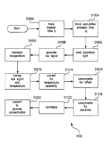
storing the time at
which the sensor was implanted (e.g., in nonvolatile storage medium 660) and
comparing the
stored time with the current time, which may, for example, be received from
the external reader
101 (e.g., with an measurement command from the external reader 101). In other
alternative
embodiments, the sensor 100 may store the time at which the sensor was
implanted, i.e., the
implant time t, (e.g., in nonvolatile storage medium 660), which may then be
read by an external
unit (e.g., sensor reader 101) for calculation of the implant time t,. As
explained in detail below,
the tracked implant time t, may be used in compensating for distortion in the
raw signal,
normalizing the raw signal, and/or converting the normalized signal Sn to a
glucose
concentration.
[0062] The process 200 may include a step S204 of tracking the cumulative
amount of
time t, that the light source 108 has emitted the excitation light 329.
Because the indicator
molecules 104 are irradiated with the excitation light 329, the cumulative
emission time te may
be equivalent to the photobleaching time tpb=
[0063] In some embodiments, the circuitry of sensor 100 includes an
emission timer
circuit that is advanced while the light source 108 emits excitation light
329. For example, in
one non-limiting embodiment, the emission timer circuit may be a counter that
increments with
each passing of a unit of time (e.g., one or more milliseconds, one more
seconds, one or more
minutes, one or more hours, or one or more days, etc.) while the light source
108 emits excitation
light 329. However, this is not required. For example, in some alternative
embodiments, the
light source 108 may emit excitation light 329 for a set amount of time for
each measurement,
24
CA 02916641 2015-12-22
WO 2015/005953 PCT/US2014/026004
and the counter may increment once for each measurement taken by the sensor
100. As
explained in detail below, the tracked cumulative emission time t, may be used
in compensating
for offset in the raw signal, compensating for distortion in the raw signal,
normalizing the raw
signal, and/or converting the normalized signal Sn to a glucose concentration.
[0064] The process 200 may include a step S206 of emitting excitation light
329. The
excitation light 329 may be emitted by light source 108. In some embodiments,
step S206 may
be carried out in response to a measurement command from the external sensor
reader 101 (e.g.,
under the control of a measurement controller). Execution of step S206 may
cause incrementing
of the tracked cumulative emission time te, which may be equivalent to the
photobleaching time
tpb=
[0065] The process 200 may include a step S208 of generating a raw signal
indicative of
the amount of light received by a photodetector (e.g., first photodetector
224). In some
embodiments, the raw signal may be generated by the first (signal)
photodetector 224. In some
non-limiting embodiments, the raw signal may be digitized by the ADC 664.
[0066] As shown in equation 3, the raw signal may contain an offset Z and
distortion
'distortion.
Signal = I + Z distortion (3)
where Signal is the raw signal generated by the photodetector, I is the
glucose-modulated
fluorescence from the indicator molecules 104, Z is an offset, and 'distortion
is distortion produced
by the indicator molecules 104 (e. g. , distortion produced by photo, thermal,
and/or oxidative
decay species of). In order to accurately calculate the glucose-modulated
fluorescence I emitted
by the indicator molecules 104, the raw signal may be purified by removing the
offset Z and the
distortion 'distortion from the raw signal. In addition, for accurate
calculation of the fluorescence
CA 02916641 2015-12-22
WO 2015/005953 PCT/US2014/026004
from the glucose indicator I, the raw signal may be corrected for temperature
sensitivity.
Accordingly, the process 200 may include steps S210, S212, S214, and/or S216
of measuring
temperature, correcting for temperature sensitivity, compensating for offset
Z, and compensating
for distortion 'distortion, respectively.
[0067] In step S210, the temperature T of the optical sensor 100 may be
measured. In
some embodiments, the temperature may be measured by the temperature sensor
670. As
explained below, in some embodiments, the measured temperature T may be used
for correcting
the raw signal for temperature sensitivity.
[0068] In step S212, the circuitry of sensor 100 may temperature correct
the raw signal
based on the temperature T of the sensor 100, which may be measured in step
S210. In
particular, in some non-limiting embodiments, the measurement controller 532
may perform the
temperature correction. As noted above, the fluorescent amplitude of the light
331 emitted by
the indicator molecules 104, as well as some elements of the circuitry within
the sensor 100 (e.g.,
light source 108), may be temperature sensitive. In one non-limiting
embodiment, the circuitry
(e.g., measurement controller 532) may correct for the temperature sensitivity
as shown in
equation 4:
[Signal] T Signal(l -4- (7' ¨ 37)c z) (4)
wherein the Signal is the raw signal generated by the photodetector (e.g.,
photodetector 224),
[Signal]T is the temperature corrected raw signal, and cz is the temperature
sensitivity of the
optical sensor. In one non-limiting embodiment, the temperature sensitivity
may simply be the
temperature sensitivity of the light source 108.
[0069] In step S214, the circuitry of sensor 100 may compensate for the
offset Z present
in the raw signal. In some embodiments, the offset Z may be hardware based.
For example, in
26
CA 02916641 2015-12-22
WO 2015/005953 PCT/US2014/026004
some embodiments, the offset Z may be related at least in part to the peak
wavelength of the
excitation light 329 emitted by the particular light source 108 used in sensor
100 and/or the
tolerance of the particular optical band-pass filter 112 used in sensor 100.
[0070] The offset Z present in the raw signal may result from excitation
light 329 emitted
from light source 108 that reaches the photodetector (e.g., first (signal)
photodetector 224). The
excitation light 329 that reaches the photodetector is convoluted in the total
light that reaches
photodetector, and, thus, produces an offset in the raw signal generated by
the photodetector.
[0071] As illustrated in FIG. 3, the excitation light 329 emitted from
light source 108 that
reaches the photodetector may include (i) a reflection light component 335
that is reflected from
the graft 106 (e.g., gel) before reaching the photodetector and (ii) a bleed
light component 337
that reaches the photodetector without encountering the graft 106. The
reflection light
component 335 may produce a reflection component Zgel of the offset Z, and the
bleed light
component 337 may produce a bleed component Zweed of the offset Z.
[0072] In some embodiments, the offset Z may be measured during the
manufacturing of
the sensor 100. However, the offset Z may increase due to photobleaching of
the indicator
molecules 104. In particular, as indicator molecules 104 become photo-
bleached, the overall
absorbance of the graft/gel 106 decreases, which increases the reflectance of
the graft/gel 106,
the amount of excitation light 329 reflected from the graft/gel 106, and the
intensity of the
reflection light component 335. Accordingly, in some embodiments, in order to
compensate for
the offset in the raw signal, the circuitry of the sensor 100 may dynamically
track the offset (e.g.,
by using the tracked cumulative emission time te).
[0073] In some embodiments, the circuitry of sensor 100 (e.g., measurement
controller
532) may compensate for the offset Z present in the raw signal by calculating
the offset Z and
27
CA 02916641 2015-12-22
WO 2015/005953 PCT/US2014/026004
removing (e.g., subtracting) the offset Z from the raw signal. For example, in
embodiments
where the raw signal is temperature corrected, the calculated offset Z may be
removed from the
raw signal by subtracting the calculated offset Z from the temperature
corrected raw signal
[Signal] r.
[0074] In one non-limiting embodiment, the circuitry of the sensor 100
(e.g.,
measurement controller 532) may calculate the offset Z as shown in equation 5:
Z Zgel + Oz ¨ e¨kPbtPb))+Z
bleed (5)
where Zgei is the component of the offset Z produced by the reflection light
component 335 (i.e.,
the excitation light 329 spillover component that is reflected from the graft
106 (e.g., gel) and
received by the photodetector), I4h is the percent increase of Zga when the
indicator is fully photo-
bleached, ko is the rate of photobleaching, to is the photobleaching time, and
Zweed is the
component of the offset Z produced by the bleed light component 337 (i.e., the
portion of the
excitation light 329 received by the photodetector that reaches the
photodetector without
encountering the graft 106). In some embodiments, the circuitry (e.g.,
measurement controller
532) may use the tracked cumulative emission time t, for the photobleaching
time to.
[0075] In step S216, the circuitry of sensor 100 may compensate for the
distortion
Ithstortion present in the raw signal. In particular, in some embodiments, the
measurement
controller 532 may perform the distortion compensation. The distortion Id
Istortion may be
chemistry (photochemistry) and kinetics based. The distortion /distortion may
be any non-glucose-
modulated light in the emission light 331 arriving at the photodetector from
the indicator
molecules 104. For example, photo, thermal, and oxidative decay species of the
indicator
molecules 104 may emit fluorescent light that is not modulated by glucose. In
fact, most of the
28
CA 02916641 2015-12-22
WO 2015/005953 PCT/US2014/026004
distortion /dolor/ton may be due to various matrix species kinetically related
to the parent indicator
BA (i.e., the active indicator species) as shown in FIG. 4.
[0076] In some embodiments, the glucose indicator molecule BA, within an in-
vivo
environment, may undergo a steady loss of signal amplitude over time. The
glucose indicator
molecule BA may be temperature sensitive. In some embodiments, oxidation,
thermal
degradation, and photobleaching may be the dominant mechanisms of the signal
degradation. In
some embodiments, the oxidation, thermal degradation, and photobleaching may
all be chronic
and predictable under a first order decay function on the loss of signal
amplitude. This decay
may establish the end of useful life for the overall sensor product. In some
embodiments, the
glucose indicator BA may be degraded by the three decay mechanisms (i.e.,
oxidation, thermal
degradation, and photobleaching).
[0077] In regard to oxidative decay species Ox, in some non-limiting
embodiments,
under in-vivo conditions, oxidation pressure from ambient and normal reactive
oxidation species
(ROS), the glucose indicator BA may progressively undergo a highly specific
oxidative de-
boronation. This reaction may remove the boronate recognition moiety of the
indicator molecule
BA. The resulting deboronated indicator (i.e., oxidized indicator Ox) may be
fluorescent (e.g., at
a lower quantum efficiency than the glucose indicator BA) and may not
modulate. Moreover,
the oxidized species Ox may be temperature sensitive and may decay due to
photo activation,
photobleaching, ancUor thermal degradation.
[0078] In regard to photo-activated decay species PA, when the oxidized
indicator Ox is
photo activated, it may produce a major product (i.e., photo-activated
oxidated species PA).
Photo-activated oxidated species PA may be fluorescent (e.g., at a higher
quantum efficiency
than oxidized species Ox) and may not modulate. Similar to the oxidized
species Ox, the photo-
29
CA 02916641 2015-12-22
WO 2015/005953 PCT/US2014/026004
activated oxidated species PA may be temperature sensitive and may decay due
to
photobleaching and/or thermal degradation.
[0079] In regard to thermal degradation product species Th, the glucose
indicator BA, the
oxidized indicator Ox, and the photo-activated decay species PA, may all
thermally degrade.
Similar to the oxidized species Ox and the photo-activated oxidated species
PA, the resulting
thermally degraded indicator Th may be fluorescent (e.g., at a lower quantum
efficiency than the
glucose indicator BA) and does not modulate. The thermal degradation product
species Th may
be temperature sensitive and may decay due to photobleaching.
[0080] The oxidated species Ox, photo-activated oxidated species PA, and
thermal
degradation product species Th illustrated in FIG. 4 are fluorescent
derivatives of the base
glucose-indicator BA. However, only the base glucose-indicator BA of the
indicator molecules
104 is a glucose modulated species. Therefore, to obtain the most accurate
measurement of
glucose concentration based on the emission light 331 received by the
photodetector, the
fluorescence /produced by the base glucose-indicator BA, which carries glucose
concentration
information, may be de-convoluted from the emission light 331, which also
include fluorescence
from the oxidated species Ox, photo-activated oxidated species PA, and thermal
degradation
product species Th. In other words, the oxidated species Ox, photo-activated
oxidated species
PA, and thermal degradation product species Th are distortion-producing
species, and the non-
glucose-modulated light /distortion from these species may be removed from the
raw signal.
Accordingly, the circuitry of the sensor 100 may track each of the distortion-
producing species
and remove them from the final signal that is converted to a glucose
concentration measurement.
CA 02916641 2015-12-22
WO 2015/005953 PCT/US2014/026004
[0081] As shown in FIG. 4, the matrix species also include completely
oxidated (i.e.,
lights out) species LO. This species LO, which is a derivative of the base
glucose-indicator BA,
has been photobleached and may not emit fluorescence.
[0082] The fluorescence ['distortion] from all the distortion-producing
species is:
[ distortion] [Ox] + [7. hi + [PA]
(8)
where [Ox], [PA], and [Th] are fluorescence from the oxidated species Ox,
photo-activated
oxidated species PA, and thermal degradation product species Th, respectively.
[0083] When the sensor is new (e.g., at manufacturing), the distortion
producing
subspecies (e.g., Ox, Th, and PA) of the indicator molecules 104 have not yet
formed and may
contribute nothing significant to the initial raw signal at turn-on. However,
the distortion 'distortion
may increase from the time the sensor 100 is inserted in vivo. In particular,
once the sensor 100
is inserted in vivo, the distortion producing subspecies (e.g., Ox, Th, and
PA) may form
progressively. Accordingly, in some embodiments, the circuitry of the sensor
100 may
kinetically track the distortion-producing species (e.g., by using the tracked
implant time ti).
[0084] In some embodiments, the circuitry of sensor 100 (e.g., measurement
controller
532) may compensate for the distortion 'distortion present in the raw signal
by calculating the
fluorescence emitted from one or more of the distortion producing species
(e.g., Ox, Th, and PA)
and removing (e.g., subtracting) the non-glucose modulated fluorescence
'distortion from the raw
signal. For example, in embodiments where the raw signal is temperature
corrected, the
calculated non-glucose modulated fluorescence /distortion may be removed from
the raw signal by
subtracting the calculated distortion 'distortion from the temperature
corrected raw signal [Signal]
[0085] In one non-limiting embodiment, the circuitry of the sensor 100
(e.g.,
measurement controller 532) may calculate the fluorescence emitted from one or
more of the
31
CA 02916641 2015-12-22
WO 2015/005953 PCT/US2014/026004
distortion producing species (e.g., oxidated species Ox, photo-activated
oxidated species PA, and
thermal degradation product species Th) as shown in equations 9-11:
b
[OX]= I0,QC%FOX (1- e¨k xt")e¨k,hithe¨kpb-phe¨k r Pa P [1¨(T ¨37)cox]
(9)
) I
[7' h] = 'O ,QC %Frii ¨ e¨khth e¨kpbt b " P 1- (77 ¨37)cThi
(10)
[PA]= io,Qc%FpA (1¨ e-koziox)e-kmtm e¨k pbt pb (
1¨ ¨37)cpAi
(11)
where lax is the fluorescence intensity of the base glucose indicator at zero
glucose
concentration h obtained from manufacturing quality control (QC); %Fox, %Fil,
and %FpA are
the relative quantum efficiencies of Ox, Th, and PA, respectively, to the base
glucose indicator
BA; kox,kih, and kph, are rates for oxidation, thermal degradation, and
photobleaching,
respectively; t0x, trb, and tpb are oxidation time, thermal degradation time,
and photobleaching
time, respectively; and co., cm, and cpA are the temperature correction
coefficients of Ox, Th and
PA, respectively. In some embodiments, the circuitry of the sensor 100 (e.g.,
measurement
controller 532) may use the tracked cumulative emission time te for the
photobleaching time tpb.
In some embodiments, the circuitry of the sensor 100 may use the tracked
implant time ti for the
oxidation time tox and thermal degradation time rth=
[0086] The process 200 may include a step S218 of normalizing the raw
signal, which in
some embodiments may have be temperature corrected, offset compensated, and/or
distortion
compensated, into a normalized signal Sn. In some embodiments, the normalized
signal Sn may
be directly proportional to glucose concentration.
32
CA 02916641 2015-12-22
WO 2015/005953 PCT/US2014/026004
[0087] In its simplest form, the normalized signal Sn may be represented
by the
following equation:
Sn = ¨
/0
(12)
where I is the glucose-modulated fluorescence from the indicator molecules 104
and lo is
baseline glucose-modulated fluorescence at zero glucose concentration.
[0088] As explained above, only the glucose-modulated fluorescence I
carries glucose
concentration information, but the raw signal generated by the photodetector
affected by
temperature sensitivity and additionally contains an offset Z and a non-
glucose modulated signal
'distortion. The raw signal may be corrected for temperature sensitivity and
the offset Z and a non-
glucose modulated signal 'distortion may be removed, and, accordingly, the
normalized signal Sn is
may be represented by the following equation:
Sn = [Signal l, ¨ Z dislonion
I (13)
where [SignaliT is the temperature corrected raw signal.
[0089] The circuitry of the sensor 100 (e.g., measurement controller 532)
may remove
noise from the raw signal and normalize it so that the normalized signal Sn
may have a constant
value at infinite glucose concentration. In other words, the normalized signal
at infinite glucose
concentration (Snff,) may not change even the indicator molecules 104 are
photobleached,
oxidate, and thermally degrade. If the noise were not removed, the noise may
compress the
modulation shown in FIG. 5 (i.e., the Y-axis displacement from zero to
infinite glucose), and the
extent to which the modulation were compressed may change based on the extent
to which the
indicator molecules 104 were photobleached, oxidated, and/or thermally
degraded.
33
CA 02916641 2015-12-22
WO 2015/005953 PCT/US2014/026004
[0090] In some embodiments, the circuitry of sensor 100 (e.g., measurement
controller
532) may normalize the glucose-modulated fluorescence I by calculating the
baseline glucose-
modulated fluorescence at zero glucose concentration (i.e., Io) and dividing
the glucose-
modulated fluorescence I by the calculated I.
[0091] In one non-limiting embodiment, the circuitry of the sensor 100 may
calculate the
baseline glucose-modulated fluorescence at zero glucose concentration lo
according to the
following equation:
I ¨ ¨ I e-kort,x e-kthith e-k p b Pb [1_ ¨ 37)C ]
0 0,QC J (14)
where 10,Qc is the /0 obtained from manufacturing quality control (QC); e e-
kthith e-koipb is the
glucose indicator decay due to the superimposition of oxidation, thermal
degradation, and
photobleaching; kox, km, and kb are rates for oxidation, thermal degradation
and photobleaching,
respectively; tox, tth, and tpb are oxidation time, thermal degradation time,
and photobleaching
time, respectively; c1 is the temperature correction coefficient of the
glucose indicator; and T is
the temperature of the optical sensor 100, which may be measured by the
temperature sensor 670
in step S210. In some embodiments, the circuitry of the sensor 100 may use the
tracked
cumulative emission time te for the photobleaching time tpb. In some
embodiments, the circuitry
of the sensor 100 (e.g., measurement controller 532) may use the tracked
implant time t for the
oxidation time tox and thermal degradation time trh. The circuitry of the
sensor 100 may be
configured to kinetically track the first order decay loss of signal that
occurs over time (e.g., by
using the tracked cumulative emission time te and tracked implant time t).
[0092] The process 200 may include a step S220 of converting the normalized
signal Sn
to a glucose concentration. The conversion of the normalized signal Sn into a
glucose
concentration may be based on the relationship between percent modulation and
glucose as
34
CA 02916641 2015-12-22
WO 2015/005953
PCT/US2014/026004
shown in FIG. 5. As described above, the percent modulation No versus glucose
concentration
may be constant throughout the life of the glucose sensor 100. The end of life
of the glucose
sensor 100 may arise when the signal to noise ratio declines over time to a
point where the error
specification can no longer be maintained.
[0093] In some embodiments, the circuitry may use an interpretive algorithm
to convert
the normalized signal Sn into glucose concentration. The interpretive
algorithm may be derived
through a standard curve based on the following reaction:
A + B BA (15)
where A is glucose indicator, B is glucose, and BA is glucose-indicator
complex. The
fluorescence of the indicator increases upon binding glucose.
[0094] The equilibrium expression for the dissociation defining Snmax
(i.e., the
normalized signal Ns at infinite glucose concentration) is
K ¨[A1B]
d [AB] (16)
[0095] The glucose concentration [A] is
[A]. K d[AB]
[B] (17)
where Kd is constant, and [AB] and [B] terms must be determined from
measurement. The
following derivation illustrates how the glucose concentration [A] may be
calculated at any one
measurement (e.g., for any normalized signal Sn) based on the relationship
shown in equations
16 and 17.
[0096] The total fluorescence F emitted by the indicator molecules 104 is:
F =FB+FAB (18)
CA 02916641 2015-12-22
WO 2015/005953 PCT/US2014/026004
where FB is the fluorescence from the unbound indicator, and FAD is the
fluorescence from the
glucose indicator complex.
[0097] According to Beer's law:
F I eebc0
(19)
where F is fluorescence of the species, /, is excitation light, e is molar
extinction coefficient, b is
path length, c is concentration of the fluorescer, and 0 is quantum
efficiency.
[0098] By substituting specifically for the concentration terms for each of
the glucose
indicator A and the glucose-indicator complex AB, the fluorescence F is:
F = I oeb[B]q5 B + 1 oeb[AB]AB (20)
[00991 By defining:
B = 0 B ([B]+ [ABD (21)
q AB = ABM+ [AB D (22)
[B]
= [B]+[AB] (23)
= [AB]
f AB r r
01+ OBI (24)
equation (20) becomes:
F = I ,eb(f Bq B f AB( I AB) (25)
[00100] The fluorescent signal value at zero glucose concentration Fõ,,õ,
which is the
lowest fluorescent signal value from the sensor, is:
Fmin = I eebq B (26)
36
CA 02916641 2015-12-22
WO 2015/005953 PCT/US2014/026004
[00101] The opposite boundary condition occurs when glucose concentration
is very high,
almost all (e.g., 99.99%) of fluorescence signal is from the glucose indicator
complex AB, and
almost none (e.g., approaching zero) of the fluorescence signal is from
unbound indicator B. The
fluorescent signal value at glucose saturation Fn., which is the highest
possible value of
fluorescence, is:
Fmax = I eebqAB (27)
[00102] By incorporating the equations for Fõ,,õ and Fm (i.e., equations 26
and 27) into
equation 25, equation 25 becomes
F = FminfB Fm.fAB = FmmfB + F.(1¨ fB)
(28)
[00103] Therefore,
./8 = Fmax ¨ F
rmax ¨ Fnu.n (29)
and
F ¨ Fmin
AB =
F max ¨ Fmin (30)
[00104] The glucose concentration [A] is:
[A]. Kd[AB] ¨
K f AB _ k."-
[B] d ''d FFmin
fB Fmax F
(31)
[00105] By substituting the normalized fluorescence Sn determined by the
circuitry of the
sensor 100 for the fluorescence F, the glucose concentration [A] becomes:
[A]=Kd
Sn¨ Snmm
Sn. ¨ Sn (32)
37
CA 02916641 2015-12-22
WO 2015/005953 PCT/US2014/026004
where the dissociation constant IQ and normalized signal at glucose saturation
Snmax may be
determined during manufacturing, the normalized signal Sn is generated by the
circuitry of the
sensor 100 by processing the raw signal generated by the photodetector of the
sensor 100, and
Snmin (i.e., 'olio) is equal to one.
[00106] The process 200 may include the step S222 of conveying the glucose
concentration to the external sensor reader 101. In some embodiments, the
glucose
concentration may be conveyed using the inductive element 114 of the sensor
100.
[00107] According to some embodiments of the invention, during sensor
manufacturing,
one or more sensors 100 may be cycled through a computer automated quality
control
measurement system. This system may measure parameters (e.g., cz, Kd, Sn,
Zgei, Zbieed). The
cycle may include operating newly manufactured sensor 100 at two different
temperatures (e.g,
32 C and 37 C) at three different glucose concentrations (e.g., OmM, 4.0mM,
and 18.0mM
glucose). The automated system may track the performance of each sensor 100
under these
changing conditions and make specific measurements for each sequential
temperature and
concentration test. In some embodiments, other parameters (e.g., Kpb, Kpa, KM)
4, cf, cm, Cox, CPA,
%Fox,%FpA and %Fm) may be developed from designed and controlled in vitro
experiments,
and still other parameters (e.g., Kox) may be developed from in vivo tests.
One or more
parameter values may be determined for each manufactured sensor 100 and used
by the circuitry
of the sensor 100 in processing a raw signal and converting the normalized
signal Sn to a glucose
concentration (e.g., according to the corresponding serial number of the
sensor 100).
[00108] In a non-limiting example of sensors that may be used to determine
a
concentration of glucose in a medium, experimental results were obtained using
eighteen sensors
incorporating one or more aspects of the present invention and implanted into
type-I diabetic
38
CA 02916641 2015-12-22
WO 2015/005953 PCT/US2014/026004
subjects. Data was collected during 6 in-clinic sessions to determine the
sensor performance and
the accuracy of the algorithm in vivo. The sensors were removed 28 days after
insertion. The
Mean Absolute Relative Difference (MARD) for all the 18 sensors from day 3
data collection
through day 28 is 13.7%. Day 0 data collection was excluded as, in some
embodiments, the
sensor may not be fully responsive to glucose during a heal-up period. A total
of 3,466 paired
data points were obtained to evaluate sensor performance, and blood glucose
measured by YSI
machine was used as a reference. FIG. 7 is a Clarke error grid showing the
3,466 paired data
points with 3328 data points (96.02%) in either the A range (i.e., values
within 20% of the
reference sensor) or the B range (i.e., values outside of 20% range but that
may not lead to
inappropriate treatment). FIG. 8 illustrates experimental results of a sensor
embodying aspects
of the present invention during six read sessions. FIG. 8 shows the
performance of one of the
implanted sensors during the six read sessions and shows that the sensor
tracks the blood glucose
well. The MARD for this sensor is 13%. Other embodiments of the sensor may be
used to
produce different results.
[00109] In some embodiments, as described above, the circuitry of the
sensor 100 (which
may, for example, include measurement controller 532) may eliminate noise
(e.g., offset and
distortions) present in the raw signal generated by the photodetector 224 and
convert the purified
raw signal into a glucose concentration, and the sensor 100 may convey the
glucose
concentration to the sensor reader 101. However, this is not required, and, in
alternative
embodiments, the sensor 100 may convey the raw signal generated by the
photodetector 224 to
the sensor reader 101, and circuitry of the sensor reader 101 (which may, for
example, include
PIC microcontroller 920) may eliminate noise present in the raw signal
generated by the
photodetector 224 and convert the purified raw signal into a glucose
concentration. For example,
39
CA 02916641 2015-12-22
WO 2015/005953 PCT/US2014/026004
in some embodiments, the circuitry of the sensor reader 101 may (i) purify the
raw signal, (ii)
normalize the purified signal to produce a normalized signal Sn that is
directly proportional to
glucose concentration, and (iii) convert the normalized signal Sn into a
glucose concentration.
[00110] FIG. 10 illustrates an exemplary raw signal purification and
conversion process
1000 that may be performed by a system including the sensor 100, which may be,
for example,
implanted within a living animal (e.g., a living human), and a sensor reader
101, which may be
external to the living animal but in the proximity of the sensor 100 (e.g., on
an armband or
wristband attached to the living animal), in accordance with an embodiment of
the present
invention. The process 1000 may include a step S1002 of tracking the amount of
time t, that has
elapsed since the optical sensor 100 was implanted in the living animal. As
noted above,
because oxidation and thermal degradation begins when the sensor 100 is
implanted, the implant
time t, may be equivalent to the oxidation time fox and the thermal
degradation time tth.
[00111] In some embodiments, the circuitry of sensor reader 101 may include
an implant
timer circuit that is started when the sensor 100 is implanted. For example,
in one non-limiting
embodiment, the implant timer circuit may be a counter that increments with
each passing of a
unit of time (e.g., one or more milliseconds, one more seconds, one or more
minutes, one or
more hours, or one or more days, etc.). However, this is not required, and, in
some alternative
embodiments, the circuitry of the sensor reader 101 may track the implant time
ti by storing the
time at which the sensor 100 was implanted (e.g., in memory 922) and comparing
the stored time
with the current time. In other alternative embodiments, the sensor 100 may
receive the time at
which the sensor was implanted, i.e., the implant time ti, from the sensor
reader 101 (e.g., when
the sensor 100 and sensor reader 101 are first linked together) and store the
received implant
time t, (e.g., in nonvolatile storage medium 660). The sensor reader 101 may
receive the time at
CA 02916641 2015-12-22
WO 2015/005953 PCT/US2014/026004
which sensor 100 was implanted from the sensor 100 for calculation of the
implant time t1. The
tracked implant time t, may be used in compensating for distortion in the raw
signal, normalizing
the raw signal, and/or converting the normalized signal Sn to a glucose
concentration.
[00112] The process 1000 may include a step S1004 of tracking the
cumulative amount of
time te that the light source 108 has emitted the excitation light 329.
Because the indicator
molecules 104 are irradiated with the excitation light 329, the cumulative
emission time te may
be equivalent to the photobleaching time tpb=
[00113] In some embodiments, the circuitry of sensor 100 may include an
emission timer
circuit that is advanced while the light source 108 emits excitation light
329. For example, in
one non-limiting embodiment, the emission timer circuit may be a counter that
increments with
each passing of a unit of time (e.g., one or more milliseconds, one more
seconds, one or more
minutes, one or more hours, or one or more days, etc.) while the light source
108 emits excitation
light 329. The count may be conveyed by the sensor 100 to the sensor reader
101. However,
this is not required. For example, in some alternative embodiments, the light
source 108 may
emit excitation light 329 for a set amount of time for each measurement, and
the counter may
increment once for each measurement taken by the sensor 100. Here again, the
count may be
conveyed by the sensor 100 to the sensor reader 101. In another alternative
embodiment, the
light source 108 may emit excitation light 329 for a set amount of time for
each measurement,
and the circuitry of the sensor reader 101 may include an emission timer
circuit that is
incremented once for each measurement command issued by the sensor reader 101
to the sensor
100 or for each measurement received by the sensor reader 101 from the sensor
100. The
tracked cumulative emission time to may be used in compensating for offset in
the raw signal,
41
CA 02916641 2015-12-22
WO 2015/005953 PCT/US2014/026004
compensating for distortion in the raw signal, normalizing the raw signal,
and/or converting the
normalized signal Sn to a glucose concentration.
[00114] The process 1000 may include a step S1006 of emitting excitation
light 329, a
step S208 of generating a raw signal indicative of the amount of light
received by a
photodetector, and/or a step S1010 of measuring the temperature T of the
optical sensor 100,
which may correspond to steps S206, S208, and S210, respectively, of the
process 200 described
above with reference to FIG. 2.
[00115] The process 1000 may include a step S1012 of conveying the raw
signal
indicative of the amount of light received by a photodetector, which may be a
digitized raw
signal, and/or the measured temperature. In some embodiments, the raw signal
and/or measured
temperature may be conveyed using the inductive element 114 of the sensor 100.
The sensor
reader 101 may receive the conveyed raw signal and/or measured temperature
(e.g., using the
inductive element 103 of the sensor reader 101).
[00116] The process 1000 may include a step S1014 of temperature correcting
the raw
signal based on the measured temperature of the sensor 100, a step S1016 of
compensating for
the offset Z present in the raw signal, a step S1018 of compensating for the
distortion 'distortion
present in the raw signal, a step S1020 of normalizing the raw signal, and a
step S1022 of
converting the normalized signal Sn to a glucose concentration. These steps
may correspond to
steps S212, S214, S216, S218, and S220, respectively, of the process 200
described above with
reference to FIG. 2, except that steps S1014, S1016, S1018, S1020, and S1022
may be
performed the circuitry of the sensor reader 101 (e.g., by the PIC
microcontroller 920) instead of
by the circuitry of the sensor 100 (e.g., by measurement controller 532).
42
CA 02916641 2015-12-22
WO 2015/005953 PCT/US2014/026004
[00117] In some embodiments, the sensor reader 101 may store (e.g., in
memory 922)
parameters specific to the sensor 100 and use the parameters during
performance of steps S1014,
S1016, S1018, S1020, and/or S1022. In some non-limiting embodiments, the
sensor reader 101
may download some or all of the parameters specific to the sensor 100 from a
web server. In
some non-limiting embodiments, the sensor reader 101 may receive some or all
of the
parameters specific to the sensor 100 from the sensor 100, which may store the
parameters (e.g.,
in nonvolatile storage medium 660) and convey the parameters to the sensor
reader 101 (e.g.,
using inductive element 114). In some embodiments, the parameters specific to
the sensor 100
may include static parameters and/or dynamic parameters. For instance, in some
non-limiting
embodiments, the parameters specific to the sensor 100 may include static
sensor parameters
(e.g., Kpb, Kpa, Kth, , cfi cm, cox, CPA, %Fox, %FpA and/or %Frh) developed
from controlled in
vitro experiments and/or static sensor parameters (e.g., Kox) developed from
in vivo tests. In
some non-limiting embodiments, the sensor reader 101 may store parameters for
only one sensor
100 at a time and be paired to a particular sensor 100 after receiving the
sensor's parameters
(e.g., by downloading them from a web server or receiving them from the sensor
100).
However, in alternative embodiments, the sensor reader 101 may store
parameters for more than
one sensor 100. For example, in one non-limiting embodiment, the sensor reader
101 may store
parameters for all of the sensors 100 with which the sensor reader 101 may be
used.
[00118] In another alternative embodiment, the circuitry of the sensor 100
(which may, for
example, include measurement controller 532) may eliminate noise (e.g.,
temperature sensitivity,
offset, and distortions) present in the raw signal generated by the
photodetector 224, the sensor
100 may convey the purified raw signal to the sensor reader 101, and the
sensor reader 101 may
convert the purified raw signal into a glucose concentration.
43
CA 02916641 2015-12-22
WO 2015/005953 PCT/US2014/026004
[00119] Embodiments of the present invention have been fully described
above with
reference to the drawing figures. Although the invention has been described
based upon these
preferred embodiments, it would be apparent to those of skill in the art that
certain modifications,
variations, and alternative constructions could be made to the described
embodiments within the
spirit and scope of the invention. For example, the circuitry of the sensor
100 and/or the sensor
reader 101 may be implemented in hardware, software, or a combination of
hardware and
software. The software may be implemented as computer executable instructions
that, when
executed by a processor, cause the processor to perform one or more functions.
44