Note: Descriptions are shown in the official language in which they were submitted.
CA 02916852 2015-12-23
WO 2015/001413
PCT/1B2014/001251
Solar cell assembly
FIELD OF THE INVENTION
The present invention relates to solar cell assemblies and to solar cell
modules
including such solar cell assemblies.
TECHNICAL BACKGROUND
Solar cells are used to convert sunlight into electricity using a photovoltaic
effect. As
shown in Fig. la, solar cell modules 100 on the basis of crystalline silicon
solar cells
may typically include 6 x 10 solar cells 104 of dimensions 15.6 x 15.6 cm2
which
may be arranged in six parallel interconnected solar cell strings. Each string
may
include ten or twelve mono- or multi-crystalline solar cells that are
connected in series
by copper ribbons 106. The strings in turn may be again connected in series by
so-
called cross-connectors 105 so that all cells in the module are connected in
series.
Solar cell modules with for example 4 x 9, 6 x 8 or 6 x 12 solar cells in the
same type
of configuration are also common.
CA 02916852 2015-12-23
WO 2015/001413
PCT/1B2014/001251
2
Under normal operation conditions, all solar cells may be illuminated and
operate at
their maximum power point of about 0.5 V. The total module voltage thereby
adds up
to about 30 V for a solar cell module of 6 x 10 solar cells. Under certain
circumstances, however, partial shading of the module can occur. When a solar
cell is
shaded, the generated electrical current decreases proportionally with the
illumination
level. Due to the series connection, the cell with the lowest current
determines the
overall current in the module. In a situation with only one cell being shaded,
this
would lead to a complete loss of power of the whole module.
To avoid such complete power loss, so-called by-pass diodes 101 may be
incorporated
into the module. The by-pass diodes are connected in parallel with a certain
number
of solar cells. In case of shading, only the cells that are in parallel with
the same by-
pass diode as the shaded cell may be affected by the power loss. The number of
by-
pass diodes per module is a compromise between the number of cells that should
be
affected by partial shading and the cost for incorporating the by-pass diodes.
Typically, two strings including 20 cells maximum are connected to one by-pass
diode. The by-pass diodes may be located in a junction box 102 that serves as
a
fixture for the cables used to connect the module to neighboring modules. Fig.
lb
shows the electrical schematics of a typical module 100 with three by-pass
diodes 101
that are mounted in the junction box 102. The strings are connected to the
junction
box by the cross-connectors 103 and are connected in series with each other by
the
cross-connectors 105 on the opposite side.
In a partial-shading situation, where only one cell 104 is completely shaded,
the by-
pass diode short-circuits all cells that are connected in parallel to the
diode. In that
situation, the illuminated cells still operate between their maximum power
point and
their open-circuit voltage at about 0.5-0.6 V each, whereas the shaded cell
does not
CA 02916852 2015-12-23
WO 2015/001413
PCT/1B2014/001251
3
generate any voltage. In contrast, the combined voltage of the illuminated
cells of 19
times about 0.5-0.6 V leads to a voltage of up to about 11.4 V being applied
to the
shaded cell in reverse bias direction.
Due to the diode-characteristic of the solar cells, there is only a negligible
reverse
saturation current flowing when a reverse bias voltage is applied. However,
the solar
cell can only withstand a certain maximum reverse bias before it comes to
avalanche
breakdown of the diode which may lead to rapid heat generation and ultimately
to the
destruction of the solar cell. Even before destruction, local shunts or "hot-
spots" may
lead to increased heat generation that can damage the module encapsulation and
even .
cause fire.
Therefore, the maXimum applied reverse bias.voltage should not exceed the
breakdown voltage of typically about 13 V. The exact breakdown voltage depends
on
the wafer material and the cell design of the solar cells. At given open-
circuit voltages
of the solar cells, the breakdown voltage limits the number of cells that can
be
connected to one by-pass diode.
The numbers above show that in the conventional module layout with cross-
connectors and junction box at the narrow side of the module, the number of
cells per
by-pass diode is already close to the maximum.
An approach to increase module,output power is to reduce the length of the
solar cells
in the direction of their interconnection with the ribbons 106, typically
achieved by
cutting the cells in half. By doing so, resistive losses, which show a
parabolic
dependence on the length of the cells, can effectively be reduced. Power
output can
be improved by around 2% with such an approach. However, the number of cells
in
each string doubles and so does the number of cells per by-pass diode.
CA 02916852 2015-12-23
WO 2015/001413
PCT/1B2014/001251
4
Another approach may be using half-cut cells and using one by-pass diode for
each
string, ie, by incorporating a connector ribbon to connect the one end of the
string
with the junction box on the opposite side. The drawback of this solution is
the power
loss of approximately 0.5 % in the connector ribbon and the substantial
additional cost
for the ribbon as well as the necessity to provide multiple back sheet layers
where the
ribbons are located to avoid shunting.
Therefore, there is a desire to have an optimal cell configuration in solar
cell modules
such that the maximum reverse breakdown voltages are not exceeded and such
that
the use of connector ribbons of excessive lengths is avoided.
SUMMARY OF THE INVENTION
A solar cell assembly is presented. The solar cell assembly includes one or
more solar
cell units coupled in series. The solar cell unit includes a first solar cell
series and 'a
second solar cell series connected in parallel. The first and second solar
cell series
include a plurality of solar cells connecting in series respectively. The
solar cell
assembly also includes a by-pass diode coupled to each solar cell unit,
wherein the by-
pass diode is coupled in parallel with the first solar cell series and second
solar cell
series respectively, i.e. the by-pass diode may be interpreted as being shared
between
the first and second solar cell series in each solar cell unit.
Objects, along with advantages and features of the present invention herein
disclosed,
will become apparent through reference to the following description and the
accompanying drawings. Furthermore, it is to be understood that the features
of the
various embodiments described herein are not mutually exclusive and can exist
in
various combinations and permutations.
CA 02916852 2015-12-23
WO 2015/001413
PCT/1B2014/001251
BRIEF DESCRIPTION OF THE DRAWINGS
In the drawings, the same reference characters generally refer to same or
similar parts
throughout the different views. Also, the drawings are only schematically and
not
necessarily to scale, emphasis instead generally being placed upon
illustrating the
principles of the invention. In the following description, various embodiments
are
described with reference to the following drawings, in which:
Figs. la-b show a layout of a solar cell module;
Figs. 2a-b show an embodiment of a solar cell assembly layout and a
corresponding
electrical schematic diagram;
Figs. 3a-b show another embodiment of a solar cell assembly layout and a
corresponding electrical schematic diagram;
Figs. 4a-b shoW yet another embodiment of a solar cell assembly layout and a
corresponding electrical schematic diagram;
Fig. 5 shows an embodiment of a junction box; and
Figs. 6a-b show an embodiment of a by-pass diode.
DESCRIPTION OF PREFERRED EMBODIMENTS
Embodiments generally relate to devices, for example, devices for converting
energy
of light into electrical energy. More particularly, the devices may be solar
cell
elements or solar cell modules including a plurality of solar cell elements.
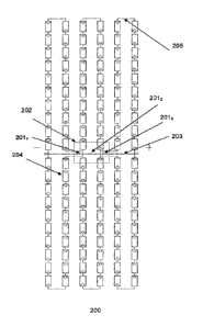
Fig. 2a shows an embodiment of a solar cell assembly layout 200 and Fig. 2b
shows a
corresponding electrical schematic diagram. In one embodiment, the solar cell
assembly is a solar cell module. In another embodiment, the solar cell
assembly is a
CA 02916852 2015-12-23
WO 2015/001413
PCT/1B2014/001251
6
portion of a solar cell module. The solar cell assembly may include solar
cells 204
which may be arranged in one or more solar cell units. As illustrated in Fig.
2a, the
solar cell assembly 200 includes three solar cell units, for example, a first
solar cell
unit 211, a second solar cell unit 212 and a third solar cell unit 213. Having
solar cell
assemblies including another number of solar cell units may also be useful.
In one embodiment, a solar cell unit includes a first solar cell series and a
second solar
cell series. For example, the first solar cell unit 211 may include a first
solar cell
series 221 and a second solar cell series 222. Within each of the solar cell
series, a
plurality of solar cells may be connected in series. For example, for a solar
cell
assembly in the form of a 6 x 10 solar cell module, the first solar cell
series may
include 10 solar cells with 15.6 x 15.6 cm2 dimensions. The solar cell series
may also
include other numbers of solar cells, for example, 12 solar cells with 15.6 x
15.6 cm2
dimensions for a 6 x 12 solar cell module may also be useful. In another
embodiment,
the solar cell unit includes solar cells cut into a plurality of sections. For
example, as
shown in Fig. 2a, the solar cells are cut into half and connected in series
with each
other within each solar cell series. By cutting the solar cells into half,
resistive losses,
which show a parabolic dependence on the length of the cells, may effectively
be
reduced. Power output may be improved by about 2%.
In one embodiment, the first and second solar cell series within the same
solar cell
unit share a same by-pass diode. The by-pass diode may include a semiconductor
material, such as silicon, with two terminals attached. The by-pass diode may
be used
to circumvent destructive effects of hot-spot heating. In one embodiment, the
bypass
diode is connected in parallel, but with opposite polarity, to a solar cell or
a group of
solar cells connected in series. Under normal operation, each solar cell in
the group
may be forward biased and the bypass diode may be reverse biased. However,
when a
CA 02916852 2015-12-23
WO 2015/001413
PCT/1B2014/001251
7
portion of the solar cell group is shaded, the bypass diode may become forward
biased
and allow the current produced by the unshaded portion to flow through the by-
pass
diode, thus avoiding the high resistance of the shaded portion and preventing
hot-spot
heating.
For example, the first and second solar cell series 221 and 222 within the
first solar
cell unit may share a first by-pass diode 2011. In one embodiment, the first
solar cell
series is connected in parallel with the second solar cell series which may
have
substantially the same open circuit voltage. Voc, as the first solar cell
series. More
particularly, the first and second solar cell series may be mirror images of
each other
with respect to the first by-pass diode. Other configurations of the first and
second
solar cell series within one solar cell unit which achieve the same Voc may
also be
useful. In one embodiment, the first by-pass diode, first solar cell series
and second
solar cell series are coupled to each other in parallel. In one embodiment,
the cathode
of the first by-pass diode may be connected to the positive nodes of both the
first and
second solar cell series, and the anode of the first by-pass diode may be
connected to
the negative nodes of both the first and second solar cell series. The
configurations of
the first and second solar cell series and by-pass diodes within other solar
cell units
may be similar to that within the first solar cell unit.
In one embodiment, the solar cell series are connected with the by-pass diodes
via
cross-connectors 203. The cross-connectors may be made of conductive materials
.
such as metals, comprising e.g. copper, aluminum, silver or alloys thereof.
For
example, the cross-connectors may be copper ribbons. Other types of conductive
materials may also be used for the cross-connectors.
CA 02916852 2015-12-23
WO 2015/001413
PCT/1B2014/001251
8
In one embodiment, the solar cells in a solar cell series are arranged in one
or more
strings connected in series. For example, for a solar cell assembly having 6 x
10 solar
cells of 15.6 x 15.6 cm2 dimensions, the first solar cell series in the first
solar cell unit
may include two strings with each string containing 5 solar cells connected in
series. =
Strings with other numbers of solar cells with other dimensions may also be
useful.
For example, as shown in Fig. 2a, for a solar cell assembly having 6 x 20 half-
cut
solar cells of 15.6 x 7.8 cm2 dimensions, the first solar cell series in the
first solar cell
unit may include two strings with each string containing 10 half-cut solar
cells
connected in series. The two strings within the first solar cell series may be
connected
in series by cross-connectors 205.
The other solar cell units within the solar cell assembly may have similar
configurations of solar cells as that in the first solar cell unit. In one
embodiment, the
solar cell units' are connected to each other in series, provided that they
generate
substantially the same output current as each other. In one embodiment, the
cross-
connectors 203 of some or all the solar cell units within the assembly are
combined as
one central cross-connector assembly and placed substantially in the centre
line of the
solar cell assembly/module as shown in Fig. 2a. Due to the symmetry of the
solar cell
assembly, it may not make a difference for the electrical device structure.
Therefore,
only a small amount of additional cross-connectors is required when compared
to the
conventional solar cell assembly/module layout, and the additional area
required for
the cross-connectors 203 and 205 is kept to a minimum. It may be important not
to
increase the area of the module during production, so that the same equipment
may be
used for producing conventional modules. In addition, module efficiency may
not be
sacrificed, which is the module power normalized to the module area and the
standard
irradiated power.
CA 02916852 2015-12-23
WO 2015/001413
PCT/1B2014/001251
9
When all solar cells, for example, in the first solar cell unit 211, operate
normally and
provide enough current to a load, the first by-pass diode 2011 coupled to the
first solar
cell unit 211 may be reverse biased, and all cells in the first solar cell
unit operate
close to a maximum power point (MPP). However, when a portion of the first
solar
cell unit becomes incapable of generating enough current for the load, for
example,
whe'n the portion of the first solar cell series is shaded from the sun or
even damaged,
the shaded or damaged portion may become reverse biased and the first by-pass
diode
2011 coupled in parallel may become forward biased to conduct currents. The
shaded
or damaged first solar cell series may not contribute to the power output of
the
assembly, while the second solar cell series which are not shaded or damaged
may
still contribute to the power output of the assembly to a small extent. This
embodiment may have better performance than the conventional configurations of
the
solar cell modules in which all solar cells connected parallel to the by-pass
diode
contribute no power when the by-pass diode is forward biased.
For example, for a solar cell assembly including 6 x 20 solar half-cut solar
cells, 10
half-cut solar cells are connected in series in one string as shown in Fig.
2a. As the
solar cell assembly is divided into three solar cell units with one by-pass
diode
coupled with one solar cell unit, this configuration allows 40 solar cells per
by-pass
diode without the maximum applied reverse bias voltage exceeding the breakdown
voltage. "Hot-spots" or destruction of solar cells may therefore be reduced.
In one embodiment, the by-pass diodes are housed in one or more junction
boxes.
Fig. 5 shows an embodiment of a junction box 550. The junction box may include
at
least one by-pass diode 501. The junction box may also include input terminal
503
for electrically coupling to respective solar cell strings and output terminal
505 for
coupling to an external device, for example, a power conditioner. In one
embodiment,
CA 02916852 2015-12-23
WO 2015/001413
PCT/1B2014/001251
.the junction box collects electrical power from both solar cell series within
some or all
solar cell units and outputs the power to the external device.
In one embodiment, as shown in Fig. 2a, all by-pass diodes in the solar cell
assembly
are mounted in a single junction box. In another embodiment, a plurality of
junction
boxes are used with each junction box containing a subset of the by-pass
diodes
coupled with the solar cell units. For example, equal number of junction boxes
as the
by-pass diodes may be used with each junction box housing one by-pass diode.
As an
illustration, three junction boxes may be used to house the three by-pass
diodes with
each junction box containing one by-pass diode. Other numbers of junction
boxes
may also be used. For example, two junction boxes may be used with a first
junction
box housing two by-pass diodes and a second junction box housing one by-pass
diode.
In one embodiment, the junction boxes are placed on the rear side of the solar
cell
assembly. The junction boxes may be disposed substantially in the centre line
of the
rear side of the solar cell assembly. For example, for a solar cell
assembly/module
including a single junction box housing all by-pass diodes therein, the
junction box
may be placed substantially in the middle of the rear side of the solar cell
assembly/module. For a solar cell assembly/module including a plurality of
junction
boxes, the junction boxes may be placed substantially in the centre line of
the rear
side of the solar cell assembly and substantially equidistant from each other
or edges
of the assembly/module. Other placements of the junction boxes which minimize
the
amount of cross-connectors may also be useful.
In yet another embodiment, a subset or all by-pass diodes in the solar cell
assembly
include integrated by-pass diodes which are integrated in a laminate of the
solar cell
CA 02916852 2015-12-23
WO 2015/001413
PCT/1B2014/001251
11
assembly/module instead of being housed in junction boxes. In one embodiment,
a
combination of junction boxes and integrated by-pass diodes are used. For
example,
for a solar cell assembly including three by-pass diodes, a combination of
junction
boxes and integrated by-pass diodes may be used. More particularly, a second
by-
pass diode may be an integrated by-pass diode integrated in the laminate of
the solar
cell assembly/module, while first and third by-pass diodes may be housed in
junction
boxes together with cross-connectors connecting to external devices or other
assemblies/modules. The second by-pass diode may be placed substantially in
the
middle of the assembly/module while the first and third by-pass diodes may be
placed
near the edges of the assembly/module.
Figs. 6a-b show an embodiment Of an integrated by-pass diode unit 650 for
being
integrated in the laminate. In one embodiment, the integrated by-pass diode
unit
includes an integrated by-pass diode 601 and two cross-connectors 605 for
coupling
to adjacent by-pass diodes or external terminals. The cross-connectors may
include
corrugation structures 655 as a stress relief to prevent the integrated by-
pass diode and
a mechanical connection between the integrated by-pass diode and the cross-
connectors from cracking due to electrical or mechanical overstresses. Other
structures for stress relief purposes may also be incorporated in the
integrated by-pass
diode unit.
It may be possible that all by-pass diodes in the solar cell assembly are
integrated by-
pass diodes as shown in Figs. 3a-b. Fig. 3a shows another embodiment of the
solar
cell assembly layout 300 and Fig. 3b shows the corresponding electrical
schematic
diagram. Features in this embodiment which are similar to that described in
Figs. 2a-
b will not be described or described in detail. In this embodiment, all by-
pass diodes
301 coupled to the solar cell units include integrated by-pass diodes which
are
CA 02916852 2015-12-23
WO 2015/001413
PCT/1B2014/001251
12
integrated into the laminate of the solar assembly/module. In such a case, two
integrated by-pass diodes near edges of the module may be connected to two
external
terminals 302 respectively to connect to an external device or other
assemblies/modules. The two external terminals may be disposed in two terminal
boxes.
This approach may have the advantage of reducing the length of the cross-
connectors
and thereby reducing the electrical losses in the cross-connectors, which
leads to an
increased module power output. On top of the higher power output, the module
area
may also be reduced which leads to an additional increase in module
efficiency.
Because the approach requires smaller amount of cross-connectors, cheaper
connector
terminals and less potting material, it may effectively reduce the module
production
cost. Since the connector terminals and cables may be located near the edges
of the
module, connecting the modules in a photovoltaic array may be facilitated. The
cables may be shorter compared to the solution with mounted junction boxes
shown in
Fig. 2a. This may result in reduced resistive losses in the cables, reduced
cost and
easier handling during installation of the modules. Instead of cable
connectors, it may
also be possible to integrate connector plugs into the sides of the module
frames to
reduce the resistive losses further.
Fig. 4a shows an embodiment of the solar cell module 400 and Fig. 4b shows the
corresponding electrical schematic diagram. Features in this embodiment which
are
similar to that described in Figs. 3a-b will not be described or described in
detail. In
one embodiment, the solar cell module includes a first solar cell assembly 431
and a
second solar cell assembly 432. The first solar cell assembly 431 includes
solar cells
of 15.6 x 3.9 cm2 dimensions. The solar cells may be obtained by cutting solar
cells
of 15.6 x 15.6 cm2 dimensions into quarters. The first solar cell assembly may
CA 02916852 2015-12-23
WO 2015/001413
PCT/1B2014/001251
13
include one or more solar cell units 412 having a first solar cell series 421
and a
second solar cell series 422. Within the solar cell series, a plurality of
solar cells may
be connected in series. For example, for a solar cell assembly with 6 x 20
solar cells
of 15.6 x 3.9 cm2 dimensions, the first solar cell series may include 20 such
solar
cells. The first solar cell series may also include other numbers of solar
cells, for
example, 24 solar cells with 15.6 x 3.9 cm2 dimensions for a solar cell
assembly with
6 x 24 solar cells of 15.6 x 3.9 cm2 dimensions. The configurations of the
solar cell
units may be similar to those described in Figs. 2a-b and Figs. 3a-b. For
example, the
first and second solar cell series with substantially the same Voc may be
connected in
parallel and share a first by-pass diode 401. More particularly, the first and
second
solar cell series may be mirror images of each other with respect to the first
by-pass
diode 401. In one embodiment, the solar cell series are connected with the
first by-
pass diodes via cross-connectors 403. The cross-connectors 403 of some or all
the
solar cell units within the first solar cell assembly may be combined as one
central
cross-connector assembly and placed substantially in the centre line of the
first solar
cell assembly. In one embodiment, connector terminals 406 are used to couple
to the
cross-connectors or central cross-connector assembly.
The configurations of the by-pass diodes and cross-connectors included in the
solar
cell assemblies in Figs. 4a-b may be similar to those described in Figs. 2a-b
and Figs.
3a-b.
In one embodiment, two solar cell assemblies are included in one solar cell
module as
illustrated in Figs. 4a-b. Other numbers of solar cell assemblies may also be
included
in the solar cell module depending on the requirements and configurations of
the solar
cells and modules. The solar cell assemblies within one solar cell mbdule may
be
connected to each other by one connector that connects the first ends and a
second
CA 02916852 2015-12-23
WO 2015/001413
PCT/1B2014/001251
14
connector that connects the second ends of the solar cell assemblies. This is
a design
that may be more tolerant to shading than conventional designs of solar cell
modules.
The invention may be embodied in other specific forms without departing from
the
scope of the invention. The foregoing embodiments, therefore, are to be
considered in
all respects illustrative rather than limiting the invention described herein.
Scope of
the invention is thus indicated by the appended claims, rather than by the
foregoing
description, and all changes that come within the meaning and range of
equivalency
of the claims are intended to be embraced therein.
Terms such as "about" in conjunction with a specific distance or size are to
be
interpreted as not to exclude insignificant deviation from the specified
distance or size
and may include for example deviations of up to 20%. Furthermore, terms such
as
"substantially parallel" or "substantially perpendicular" are to be
interpreted as not to
exclude insignificant deviation from the specified arrangement and may include
for
example deviations of up to 20 .
Finally, it should be noted that the term "comprising" does not exclude other
elements
or steps and the "a" or "an" does not exclude a plurality. Also elements
described in
association with different embodiments may be combined. It should also be
noted
that reference signs in the claims should not be construed as limiting the
scope of the
claims.