Note: Descriptions are shown in the official language in which they were submitted.
CA 02917147 2015-12-30
WAVELENGTH-TUNABLE VERTICAL CAVITY SURFACE EMITTING
LASER FOR SWEPT SOURCE OPTICAL COHERENCE TOMOGRAPHY
SYSTEM
TECHNICAL FIELD
[0001] The technology described herein generally relates to optical
coherence
tomography systems, and more particularly relates to such systems based on
vertical
cavity surface emitting laser devices.
BACKGROUND
[0003] Optical Coherence Tomography (OCT) is a technique for high-
resolution depth
profiling of a sample (biological samples such as tissues, organs, living
bodies, or industrial
samples such as polymers, thin-films). There are two types of OCT, namely, a
time-
domain OCT (TD-OCT), and a frequency-domain OCT (FD-OCT). In TD-OCT, the
broadband light source is typically a superluminescent diode, which
simultaneously emits
multiple wavelengths; by scanning the position of a reference mirror, the
frequencies of
interference components in the reflecting light from the sample are analyzed.
In FD-OCT,
a swept source type OCT (SS-OCT), which employs a wavelength tunable laser as
the
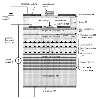
broadband source, has become more widely used. In SS-OCT, only one wavelength
is
present at any one time, and sweeping of the laser wavelength replaces the
mechanical
scanning of the reference mirror. The signal to noise ratio of SS-OCT is
fundamentally
better than that of TD-OCT.
[0004] For a tunable laser for use in SS-OCT, requirements include: single-
mode
operation, a wide tuning range, high scan rate of wavelength, and wavelength
tuning that is
a simple monotonic function of a tuning control signal.
¨ 1 ¨
CA 02917147 2015-12-30
WO 2015/003023 PCT/US2014/045170
[0005] A tunable VCSEL with a MEMS that utilizes two distributed Bragg
reflectors
(DBR) has been reported. Such a device employs a bottom mirror consisting of a
lower
DBR composed of multiple alternating layers of AlGalnAs and InP, and an active
layer
composed of InP-based multiple quantum wells (MQWs) and barriers, which are
all grown
on a InP substrate, and a MEMS tunable upper DBR. The device has a tuning
range of 55
nm at a center wavelength around 1550 nm. This tuning range is not sufficient
for a number
of applications.
[0006] FIG. 1 illustrates such a tunable VCSEL with MEMS, as known in the
art. On a
InP substrate 1, a n-doped distributed Bragg reflector (DBR) 2 consisting of
over 40 pairs
(not all shown) of alternating layers of AlGalnAs 2a (lattice-matched to InP)
and InP 2b are
epitaxially grown, followed by a n-type AlGalnAs cladding layer 3. On the top
of the
cladding layer 3, an active layer 4 consisting of multiple (six) AlGalnAs
quantum wells
("QWs") 4a and multiple (seven) AlGalnAs barriers 4b are grown, followed by a
p-type
AlGalnAs cladding layer 5. Above the p-type cladding layer 5, a p++-doped-
AlGalnAs / n++-
doped-AlGalnAs tunnel junction layer 6 is grown to allow the replacement of a
p-type InP
layer with a n-doped InP layer since the tunnel junction can convert electrons
to holes,
which is followed by a n-doped InP layer 7 and a n++-doped GalnAs contact
layer 8. VCSEL
p-electrode 9 is formed on the top of the contact layer 8 and n-electrode 10
is formed on the
substrate 1, to complete the "half VCSEL" structure. On the top of the half
VCSEL structure,
an independently manufactured upper mirror part is bonded to the half VCSEL
structure.
The independently manufactured upper mirror part is formed on a "handle" Si-
substrate 11
that bonds the two layers together. A 5i02 layer 12 is formed as an insulation
layer,
followed by a beam support layer of Si 13. A thin membrane 14 is formed by
etching the
5i02 layer 12 as a sacrificial layer. An upper dielectric DBR 15 is deposited
on one side of
the membrane 14, and an antireflection (AR) coating 16 is deposited on the
opposite side.
A MEMS electrode 17 and Au-bumps 18 are formed to supply the MEMS voltage,
which can
change the air gap between the contact layer 8 and the upper DBR 15. An
electric voltage
source 19 is connected with the MEMS electrode 17 and with the p-electrode 9.
Therefore,
the membrane 14 can be moved by the electrostatic force induced by the
electric voltage
source 19, thereby changing the cavity length formed between the upper and
bottom DBR
¨2¨
CA 02917147 2015-12-30
mirrors, which in turn changes the lasing wavelength. An electric current
source 20 is
connected for current injection to the half VCSEL part.
[0007] Details of a device such as in FIG. 1 are described in T. Yano, H.
Saitou, N.
Kanbara, R. Noda, S. Tezuka, N. Fujimura, M. Ooyama, T. Watanabe, T. Hirata,
and
Nishiyama, "Wavelength modulation over 500 kHz of micromechanically tunable
InP-based
VCSELs with Si-MEMS technology", IEEE J., Selected Topics in Quantum
Electronics, vol.
15, pp. 528-534, May/June 2009. VCSEL's with fixed lasing wavelengths of 1310
nm and
1550 nm, utilized in the prior art, are described in N. Nishiyama, C. Caneau,
B. Hall, G.
Guryanov, M. H. Hu, X. S. Liu, M.-J. Li, R. Bhat, and C. E. Zah, "Long-
wavelength vertical-
cavity surface-emitting lasers on InP with lattice matched AlGalnAs-InP DBR
grown by
MOCVD", IEEE J., Selected Topics in Quantum Electronics, vol. 11, pp. 990-998,
Sept./Oct. 2005.
[0008] In the prior art configuration of FIG. 1, a tuning range of 55 nm at
a center
wavelength around 1550 nm has been shown. The maximum tuning range is limited
by the
reflectivity bandwidth of the bottom DBR, which is determined by the ratio of
the refractive
indices of high-index and low-index materials. The reflectivity bandwidths of
a DBR
composed of alternating layers of AlGalnAs (high-index material) and InP (low-
index
material) are approximately 50 nm and 70 nm for center wavelengths of 1310 nm
and 1550
nm, respectively. However, SS-OCT requires over 100 nm tuning range.
Therefore, the
VCSEL employing a DBR composed of AlGalnAs and InP and an active layer
comprising
quantum wells is not suitable for OCT applications.
[0009] To overcome this tuning range limitation, a tunable VCSEL with MEMS
has been
suggested, that employs a bottom mirror consisting of a DBR composed of
alternating
layers of AlGaAs (high-index material) and Alx0y (low-index material) that has
a reflectivity
bandwidth over 200 nm centered near 1300 nm. This type of tunable VCSEL has
achieved
a tuning range over 100 nm by optical pumping. The details are described in V.
Jayaraman, J. Jiang, H. Li, P. J. S. Heim, G. D. Cole, B. Potsaid, J. G.
Fujimoto, and A.
Cable, "OCT imaging up to 760 kHz axial scan rate using single-mode 1310 nm
MEMS-
tunable VCSEL with >100 nm tuning range", CLEO: 2011 ¨ Laser Science to
Photonic
Applications, PDPB2, 2011. In this approach, the active region comprises InP
based
¨3¨
CA 02917147 2015-12-30
multiple quantum wells (MQWs) epitaxially grown on an InP substrate. The
bottom DBR is
epitaxially grown on a GaAs substrate. Therefore, the materials in the active
region and
the DBR part cannot be grown on a single type substrate. The two wafers must
be bonded
together, and then the InP substrate needs to be removed in order to form the
half VCSEL
part. Bonding the GaAs and InP wafers and the removing the InP wafer requires
a very
complicated process and introduces potential reliability issues.
[0010] Quantum dot (QD) lasers have been investigated with the aim of
replacing
conventional quantum-well lasers. QD lasers have unique characteristics such
as ultra-low
threshold currents and low temperature sensitivity due to the three-
dimensional quantum
size effect. Quantum dot technology has progressed significantly by the self-
assembling
growth technique of InAs QD's on large GaAs substrates. Application of QD's to
conventional edge emitting lasers (as opposed to VCSEL systems) has been
accomplished
by replacing quantum wells of the active layer by QD's. The high performance
of 1.3 pm
QD Distributed Feedback (DFB) lasers has been reported recently. These lasers
are
fabricated by molecular beam epitaxy (MBE) of 8 stacks of a high density QD
layer with p-
doped GaAs layers on a p-type GaAs substrate. The gain spectrum has been
measured: a
maximum net modal gain as high as 42 cm-1 at around 1280 nm is obtained, and
the 3 dB
gain bandwidth is approximately 65 nm. The details are described in K. Takada,
Y.
Tanaka, T. Matsumoto, M. Ekawa, H. Z. Song, Y. Nakata, M. Yamaguchi, K. Nishi,
T.
Yamamoto, M. Sugawara, and Y. Arakawa, "10.3 Gb/s operation over a wide
temperature
range in 1.3 pm quantum-dot DFB lasers with high modal gain", Optical Fiber
Communication Conference\National Fiber Optic Engineers Conference, (2010),
Technical
Digest.
[0011] A 1.3 pm VCSEL comprising QD's for fixed wavelength applications has
also
been reported recently: On a GaAs substrate, a bottom DBR composed of 33.5
pairs of n-
doped AlGaAs layer and ntdoped GaAs layer, an undoped active region composed
of
InAs/InGaAs QD's, a p-doped AIGaAs oxidation layer, and a upper DBR composed
of 22
pairs of ptdoped AlGaAs layers and ptdoped GaAs layers, are grown by MBE. The
lasing wavelength is around 1279 nm at room temperature. A small linewidth
enhancement factor of 0.48 has also been reported, which can provide a narrow
linewidth
¨4¨
CA 02917147 2015-12-30
that is critical for OCT applications. The details are described in P.-C.
Peng, G. Lin, H.-C.
Kuo, C.E. Yeh, J.-N. Liu, C.-T. Lin, J. Chen, S. Chi, J. Y. Chi, S.-C. Wang,
"Dynamic
characteristics and linewidth enhancement factor of quantum-dot vertical-
cavity surface-
emitting lasers", IEEE J. Selected Topics in Quantum Electronics, vol. 15, pp.
844-849,
May/June 2009.
[0012] The discussion of the background herein is included to explain the
context of the
technology. This is not to be taken as an admission that any of the material
referred to was
published, known, or part of the common general knowledge as at the priority
date of any
of the claims found appended hereto.
[0013] Throughout the description and claims of the specification the word
"comprise"
and variations thereof, such as "comprising" and "comprises", is not intended
to exclude
other additives, components, integers or steps.
SUMMARY
[0014] The present disclosure describes a microelectromechanical system
(MEMS)
tunable vertical cavity surface-emitting laser (VCSEL) comprising one or more
layers of
quantum dots.
[0015] The present disclosure describes a novel MEMS tunable quantum dot-based
VCSEL swept source design having a narrow dynamic line width with a wide
tuning range,
necessary for deeper tomographic imaging with higher axial resolution. One
embodiment
provides a MEMS tunable quantum dot VCSEL that solves at least two problems in
the
prior art: (1) insufficient DBR reflectivity bandwidth of InP based DBR, and
(2) complicated
wafer bonding required for two different types of wafers, (as in, for example,
an InP based
active region wafer and a GaAs based DBR wafer). In one embodiment, a GaAs
based
DBR with high reflection bandwidth and an active region of optical gain peak
wavelength
(including an exemplary embodiment centered around 1300 nm) can be epitaxially
grown
on a GaAs substrate, continuously without wafer bonding.
[0016] The MEMS tunable VCSEL includes an upper vertically movable mirror part
and
a bottom half VCSEL part. The upper mirror part includes: a membrane part
supported by
¨5¨
CA 02917147 2015-12-30
suspension beams, and an upper DBR provided on the membrane for reflecting
light. The
bottom half VCSEL part includes a bottom GaAs based DBR, an active region
consisting of
quantum dots which are epitaxially grown on top of the bottom DBR, and formed
in a
position facing the top DBR layer of the top mirror part via a gap. The cavity
length of the
cavity formed between the upper DBR and the bottom DBR can be changed by
changing
the gap distance through application of an electrostatic force to the
membrane. Therefore,
the lasing wavelength can be continuously changed with high speed. Since the
VCSEL
oscillates in a single mode, sample detection sensitivity is high in that the
internal
detectable depth is as deep as 50 mm in the SS-OCT system.
[0016a] In one embodiment there is provided a microelectromechanical system
(MEMS)
tunable vertical cavity surface-emitting laser (VCSEL) including an air gap,
an anti-
reflective (AR) coating, and one or more layers of quantum dots situated in
between an
upper and a lower distributed Bragg reflector (DBR). The VCSEL has a tunable
range of
greater than 100 nm.
[0016b] The one or more layers of quantum dots may include InAs or InGaAs
quantum
dots, and may be separated by InGaAs barrier layers.
[0016c] Each of the DBRs may include multiple pairs of alternating layers of
material.
[0016d] The one or more layers of quantum dots may be in an active region
grown
continuously on the lower DBR.
[0016e] In accordance with another embodiment there is provided an optical
coherence
tomography system including the tunable VCSEL described above.
[0016f] The alternating layers of material may include GaAs or AlGaAs.
[0016g] In another embodiment there is provided a tunable VCSEL for swept
source
optical coherence tomography including a MEMS tunable VCSEL. The MEMS tunable
VCSEL includes a bottom half VCSEL part, and an upper mirror part. The bottom
half
VCSEL part includes a bottom distributed Bragg reflector (DBR) that is
epitaxially grown on
a semiconductor substrate, and an active layer comprised of a plurality of
layers of
¨6¨
CA 02917147 2015-12-30
quantum dots that are epitaxially grown on the top of the bottom DBR. The
upper mirror
part includes a handle substrate, a vertically movable membrane supported by
beams, and
supporting the handle substrate, an upper distributed Bragg reflector provided
on the
vertically movable membrane, as an upper reflector for light, and electrodes
supplying a
voltage between the vertically movable membrane and the handle substrate to
change a
cavity length of a cavity formed between the upper distributed Bragg reflector
and the
bottom distributed Bragg reflector.
[0016h] The active layer may include multiple layers including more than one
size of
quantum dot.
[00161] The active layer may include multiple layers including more than one
composition of quantum dot.
[0016j] The active layer may include multiple layers consisting of quantum
dots having a
second quantized energy state.
[0016k] The active layer may include multiple layers consisting of InAs or
InGaAs
quantum dots.
[00161] The active layer may include multiple layers of quantum dots having a
center
wavelength in the range of 250-1950 nm.
[0016m] The active layer may include multiple layers of quantum dots having a
center
wavelength in the range of 850-1700 nm.
[0016n] The active layer may include multiple layers of quantum dots having a
center
wavelength in the range of 1100 ¨ 1350 nm.
[00160] The semiconductor substrate may include GaAs.
- 6a -
CA 02917147 2015-12-30
BRIEF DESCRIPTION OF THE DRAWINGS
[0017] FIG. 1 is a schematic of a prior art MEMS tunable VCSEL;
[0018] FIG. 2 is a schematic representation of a MEMS tunable quantum dot
VCSEL
according to one exemplary embodiment;
[0019] FIG. 3 is a schematic representation of a MEMS tunable quantum dot
VCSEL
according to a second exemplary embodiment;
[0020] FIG. 4a is a top view of an upper mirror part of a MEMS tunable
VCSEL
according to an embodiment;
[0021] FIG. 4b is a cross-section view along the A¨A line of the upper
mirror part in the
embodiment of FIG. 4a;
[0022] FIG. 5 is a schematic representation of a swept source optical
coherence
tomography system (SS-OCT) based on a MEMS tunable quantum dot VCSEL;
[0023] FIG. 6a is a schematic of a fiber based MEMS tunable quantum dot VCSEL
swept source; and
[0024] FIG. 6b is a schematic of a free space based MEMS tunable quantum
dot
VCSEL swept source.
- 6b -
CA 02917147 2015-12-30
[0025] Like reference symbols in the various drawings indicate like
elements.
DETAILED DESCRIPTION
[0026] The technology of the present disclosure is exemplified by the two
embodiments
shown in FIGS. 2 and 3, respectively. Each embodiment in FIGS. 2 and 3
comprises a pair
of DBR's, one in the lower VCSEL half, and one in the upper MEMS portion. The
two
embodiments differ in the configuration of the upper (MEMS) half of each
device. Both
upper portions have the same overall function, and contain a membrane, an air
gap and an
upper (dielectric) DBR. The laser frequency is generated from a combination of
the two
DBR's and the air gap in between them.
[0027] FIG. 2 shows a schematic of an exemplary embodiment of the MEMS tunable
quantum dot VCSEL. On GaAs substrate 321, a n-doped DBR 322 consisting of 30
to 40
pairs of alternating layers of GaAs 322a, and AIGaAs 322b lattice matched to
GaAs, is
epitaxially grown, followed by a n-doped GaAs cladding layer 323. Then, an
active layer
324 consisting of multi-layer stacks of InAs quantum dots (QD's) 324a (for
example, lateral
size of about 20 nm and a height of about 5 nm) alternating with InGaAs
barrier layers
324b, are grown, followed by a p-doped AIGaAs cladding layer 325. Other size
quantum
dots are acceptable, for example having an average diameter of 5 ¨ 8 nm,
though may be
nm in size or up to 30 nm. The dot density in each layer 324a is typically in
the range
1010 ¨ 1011 dots/cm2. This is expressed as a "surface area density", since
each layer
typically supports only a single layer of dots. There are typically 8 ¨ 20
layers per stack in
the active layer, where each layer is up to about 40 nm thick, preferably 10 ¨
30 nm thick.
Other numbers of layers are also consistent with the devices herein. The
quantum dots are
preferably made from InAs, though may be made from InGaAs, consistent with the
operation of the overall technology. Quantum dots thereby provide different
properties and
functions in the active layer, when compared to the quantum wells previously
used in the
art. The quantum dots in the active layers may consist of dots of different
sizes, as well as
different compositions. In some embodiments, the quantum dots have a second
quantized
energy state (that is beneficial because it broadens the available spectrum to
shorter
wavelengths).
- 7 -
CA 02917147 2015-12-30
[0028] Above the cladding layer 325, an AlGaAs oxidation layer 326 and a
further p-
doped AIGaAs cladding layer 325a are grown. The oxidation layer 326 is partly
oxidized
except in a center region, referred to as aperture 326a having a diameter of 3
to 8 pm, to
which an injection current (from 325a to the center region of 325) is confined
(326 inhibits
the current flow due to oxidation). On the top of cladding layer 325a, a p-
doped GaAs
contact layer 327 is grown. VCSEL p-electrode 328 and n-electrode 329
(typically made of
Ti, Pt, or Au and Cr, Ni, or Au respectively) are formed on the top of the
contact layer 327
and the bottom of substrate 321, respectively, to complete a half VCSEL
structure.
[0029] After depositing an anti-reflection (AR) coating 51 on the GaAs
contact layer 327,
the top half MEMS is formed by depositing a spacer layer 52, composed of, for
example,
amorphous Ge, which is followed by a frame structure 53, composed of, for
example,
silicon nitride (SiNx). A membrane 54 is formed by etching the spacer layer
52. In FIG. 2,
items 53 and 54 correspond to frame structure 332, and to membrane 333,
respectively, in
Fig. 4(a). An upper dielectric DBR 55, comprised of alternating layers of, for
example, TiO2
and Si02, or A1203 and a-Si (amorphous silicon), is deposited on one side of
the membrane
54. A MEMS electrode 56 is formed on frame structure 53. An electric voltage
source 57
is connected between the electrode 56 and the p-metal (typically Ti, Pt or Au)
electrode
328, to supply a MEMS voltage. Therefore, the membrane 54 can be deflected
vertically
by the electrostatic force induced by the voltage source 57. This deflection
can change the
cavity length formed between the upper DBR 55 and the bottom DBR 322, which
changes
the lasing wavelength. It is to be understood that where particular materials
are specified
for various layers and portions of the structure in FIG. 2, other materials
having equivalent
functions and properties could be used in their place, according to
considerations
understood to those of skill in the art.
[0030] FIG. 3 shows a schematic of another exemplary embodiment of the MEMS
tunable quantum dot VCSEL. On GaAs substrate 321, a n-doped DBR 322 consisting
of
30 to 40 pairs of alternating layers of GaAs 322a, and AlGaAs 322b lattice
matched to
GaAs, is epitaxially grown, followed by a n-doped GaAs cladding layer 323.
Then, an
active layer 324 consisting of multi-layer stacks of InAs quantum dots (QD's)
324a (for
example, lateral size of about 20 nm and a height of about 5 nm) alternating
with
- 8 -
CA 02917147 2015-12-30
PCT/US14/45170 04-05-2015 PCT/US2014/045170 17.06.2015
/
PCT/US14/45170
Attorney docket no.: 1465-00-002W01
REPLACEMENT SHEET
InGaAs barrier layers 324b are grown, foilowed by a p-doped AlGaAs cladding
layer 325.
Above the cladding layer 325, an AlGaAs oxidation layer 326 and a p-doped
AlGaAs layer
325a are grown. The oxidation layer 326 is partly oxidized except in a center
region,
referred to as aperture 326a, having a diameter of 3 - 8 pm, to which an
injection current
=
(from 325a to the center region of 325) is confined. The oxidation layer 326
inhibits the
current flow because the oxide is a poor conductor. On the top of the cladding
layer 325a, a
p-doped GaAs contact layer 327 is grown, and thereafter an anti-reflection
(AR) coating 336
is deposited on the GaAs contact layer 327.
[0031] VCSEL p-electrode 328 and n-electrode 329 are formed on the top of the
contact
layer 327 and the bottom of substrate 321, respectively, to complete a half
VCSEL structure.
To the extent thus far described, the structure of FIG. 3 is the same as that
in FIG. 2. In the
= embodiment of FIG. 3, on the top of the half VCSEL structure, an
independently
= manufactured top mirror part is bonded with a method such as thermo-
compression The
embodiment of FIG. 3 is therefore made differently from that of FIG. 2: in
FIG. 2, the device
can be manufactured from the bottom all the way up to the topmost layer (i.e.,
based on a
single substrate). The device of FIG. 3, by contrast, is made in two pieces.
The bottom half
of the VCSEL is deposited on the substrate, layer by layer, whereas the upper
IVIEMS
portion is made separately, and then attached to the bottom half.
[0032] FIG. 4a is a top view of a vertically movable upper mirror
part of a VCSEL
according to the embodiment of FIG. 3. FIG. 4b is a cross-sectional view along
the A¨A
line of FIG. 4a. The portion shown in FIG. 4b corresponds to the upper part of
the device of '
FIG. 3; it is shown inverted relative to FIG. 3 in order to illustrate the
manner in which it is
made (by deposition of layers on to a substrate 330 that then becomes the top
of the
device). The movable upper mirror part is formed on a handle Si-substrate 330,
as follows.
The MEMS part is made independently from the half VCSEL part, and bonded
through the
Au bumps 338 to the half VCSEL part. The Si-substrate 330 thereby functions
like a kind of
handle for bonding the two parts to one another. A SiO2 layer 331 is formed as
an insulation
layer, followed by a frame structure L. A thin circular membrane 333 is
formed, supported
by four suspension beams 334 (FIG. 4a), which are formed by etching the SiO2
layer 331 as
a sacrificial layer. An upper dielectric DBR 335, comprised of alternating
layers of, for
example, TiO2 and Si02, or A1203 and a-Si, is deposited on one side of the
membrane 333.
905907_1 - 9 ¨
=
=
AMENDED SHEET - IPEA/US
CA 02917147 2015-12-30
PCT/US14/45170 04-05-2015
PCT/US2014/045170 17.06.2015.
PCT/US14/45170
Attorney docket no.: 1465-00-002W01
REPLACEMENT SHEET
As shown in FIG. 3, a MEMS electrode 337 is formed on the substrate 330, and
gold (Au)
bumps 338 are formed on membrane 333. Typically, within the upper MEMS part,
layers
331, 332/333 and 338 are formed in sequence on the Si substrate 330.
[0033] The upper mirror part (shown in Fig 4a) is bonded to the p-
electrode 328 via Au
bumps 338 (with a method such as thermo-compression). An electric voltage
source 339 is
connected between the MEMS electrode 337 and the p-metal (typically Ti, Pt or
Au)
electrode 328, to supply a MEMS voltage. Therefore, the Membrane 333 can be
deflected
= vertically by the electrostatic force induced by the voltage source 339.
This deflection can
change the cavity length formed between the upper DBR 335 and the bottom DBR
322,
which thereby changes the lasing wavelength. An electric current source 340 is
connected
= to provide current injection to the active region 324. It is to be
understood that where
particular materials are specified for various layers and portions of the
structures in FIGS. 3,
4a and 4b, other materials having equivalent functions and properties could be
used in their
place, according to considerations understood to those of skill in the art.
[0034] FIG. 5 shows a schematic of a swept source optical coherence
tomography
system (SS-OCT) based on a MEMS tunable quantum dots VCSEL swept source
utilizing a
MEMS tunable quantum dot VCSEL such as shown in FIGs. 2, and 3, 4a and 4b. In
this
embodiment, the MEMS tunable quantum dots VCSEL swept source 100 has an
optical
output 209 that is then divided into two parts via fiber optic *coupler 101.
One division Of
wave output is directed through a circulator 102 to a sample arm 103. Another
division from
the fiber optic coupler 101 is directed through circulator 104 to reference
arm 105.
Reflected wave from sample arm 103 and reference arm 105 are recombined
through fiber
optic coupler 106, and the recombined wave is detected by balance detector 107
to give
interference signal 112. Wavelength monitoring/k-clock output 210 is divided
in two parts
through fiber optic coupler 108 and recombined through fiber optic coupler 109
that is
detected by balance detector 110 to give k-clock signal 111. A data
acquisition card (DAQ)
113 is used to collect interference signal 112 and k-clock signal 111, and a
reconstructed
depth profile is displayed through processing and display module 114.
Components such
905907_1 =
¨ 10 ¨
AMENDED SHEET - IPEA/US
CA 02917147 2015-12-30
as couplers, balance detectors, and circulators, are typically off-the-shelf
components that
can be used with the technology described herein with little modification.
[0035] Regarding the MEMS tunable quantum dots VCSEL swept source 100 shown in
FIG. 5, there are two exemplary embodiments (fiber based and free space
based). FIG. 6a
shows a schematic of an exemplary fiber based MEMS tunable quantum dots VCSEL
swept source (100a). This embodiment comprises quantum dot tunable VCSEL 201
(such
as one shown in FIG. 2, or in FIGS. 3, 4a and 4b), isolator 202, fiber optic
coupler 203,
semiconductor optical amplifier (SOA) 206, isolator 207 and fiber optic
coupler 208.
Optical output 209a and another output for wavelength monitoring / k-clock
210a comes
from fiber optic coupler 208. An additional output from coupler 203 can be
added for post
amplification wavelength monitoring 205, and a polarization control 204 can be
used to
maximize power after amplification through SOA 206. Items 202, 203, 206, 207,
208,
209a, and 210 are off-the-shelf items that can be used without much
modification.
[0036] FIG. 6b shows a schematic of an exemplary free-space based MEMS tunable
quantum dot VCSEL swept source (100b) that produces optical output 209b. This
embodiment comprises a MEMS tunable quantum dot VCSEL 201 (such as one shown
in
FIG. 2, or in FIGS. 3, 4a and 4b), isolator 211, SOA 212, isolator 213, and a
beam splitter
214. In this embodiment, two outputs, optical output 215b and wavelength
monitoring / k-
clock 210b, are created by the beam splitter 214. Items 211, 212, 213, 214,
215b, and
210b are off-the-shelf items that can be used without much modification.
Tunable Wavelength Range
[0037] The combination of a QD active region and a MEMS tunable DBR, as
described
herein and exemplified in FIGS. 2 and 3, has not previously been reported. The
tunable
wavelength range of the swept source from such a combination is preferably
greater than
100 nm. Typically, the tunable wavelength range of a single swept source is
from 100 ¨
200 nm, i.e., may be up to 110 nm, up to 120 nm, up to 150 nm, up to 180 nm.
Variations
are achieved by altering, for example, the compositions of the quantum dots,
or by using
combinations of quantum dots of different compositions. The tunable range is
typically
centered on one of three or four different bands, including but not limited to
center
- 11 -
CA 02917147 2015-12-30
wavelengths from 250 ¨ 1950 nm for example at: 850 nm; 1,050 nm (sometimes
loosely
referred to as "1 micron"); 1,300 nm; 1,500; and 1,700 nm. The relevant
applications of
different center wavelengths depend on the tissue or other material that is
being analyzed
by the laser light produced by the device. The present embodiment is able to
achieve the
stated tuning range, as explained hereinbelow.
[0038] The peak wavelength of the optical gain of a QD is determined by the
size and
shape of the QD and its composition, as well as the barriers surrounding the
QD. Although
the shape of a real QD is not a rectangular solid, the gain peak wavelength
for a QD
formed with size axbx c along the x-, y- and z-directions respectively, can be
calculated
relatively straightforwardly as follows: the emission wavelength corresponding
to the
transition between the quantized energy levels of the conduction and valence
bands with
the same quantization number is given by equation (1):
2(,um)= 1.24 /(Eg + .E7n1 + (1)
where E'n' and E"7. are quantized energy levels in the conduction and valence
band of
the QD, respectively. The gain peak wavelength is a little shorter than the
emission
wavelength given by equation (1) due to the carrier related broadening effect.
If an infinite
barrier potential for the QD is assumed for the sake of simplicity, Ecn" and
E'w can be
expressed analytically as:
= + h2 *[(17r)2 +(mg)2 + __ (rig vi
2m a b c
(2)
h2 [11'7'12 mi r
Evrn"' = Evo
2mh L a ) b ) c j (3)
where Eco is the conduction-band edge energy, Evo is the valence band edge
energy,
m: and mh* are the effective mass of the electrons and the holes,
respectively, h is "h-bar"
(the Planck constant h divided by 24 Integers /, m, and n are quantum numbers
that
denote the labels of the quantized energy levels. The lowest energy level
corresponds to /
- 12 -
CA 02917147 2015-12-30
= m = n =1 (or I' = m' = n' = 1). The gain peak appears around the quantized
energy level.
Therefore, the gain peak wavelength is determined by the dot size, and the
dimensions a,
b and c. In this way, the gain peak wavelength can be changed by changing the
size of a
QD. A QD with larger size has a second quantized state (either of /, m, or n
(or m', n) is
larger than 1) with higher energy that has a gain peak at shorter wavelength
side. These
two gain peaks make a broad gain spectrum.
[0039] The detail of the gain spectrum of QD's is described in (S. L.
Chuang, Physics of
Photonic Devices, John Wiley & Sons 2009, pp. 376 ¨ 381As noted in equations
(1) and
(2), the energy levels are also determined by the effective masses m: and in:
of the
carriers, and the band edge energies Ed, and E,,0, which are related to the
compositions of
the QD's and the respective barriers. The size and shape of QD's in each QD
layer can be
adjusted by varying crystal growth condition and composition selection:
therefore, the gain
peak wavelength can have a distribution which will produce a broader gain
spectrum. A
gain bandwidth of 65 nm has been reported in the publication Takada, et al.,
"10.3 Gb/s
operation over a wide temperature range in 1.3 pm quantum-dot DFB lasers with
high
modal gain", Optical Fiber Communication Conference\National Fiber Optic
Engineers
Conference, Technical Digest (2010).
[0040] In other work, the gain bandwidth of QD's can further be broadened
by
combining QD's and a quantum well (QW): the quantized energy level of the QW
is
chosen to be higher than the second quantized energy level of the QD,
providing another
gain peak to broaden the gain bandwidth. Using this method, a total gain
bandwidth of
more than 200 nm has been achieved. In this work, a gain bandwidth of 160 nm
from QD's
alone was shown. The detail is described in (S. Chen, K. Zhou, Z. Zhang, J. R.
Orchard,
D. T. D. Childs, M. Hugues, O. Wada, and R. A. Hogg, "Hybrid quantum
well/quantum dot
structure for broad spectral bandwidth emitters", IEEE J. Selected Topics of
Quantum
Electron., vol. 19, No.4, July/Aug. 2013). But the structures described in the
two
references cited in this and the preceding paragraph are not sufficient to
achieve the lasing
wavelength tuning of a widely tunable laser or a swept source.
- 13 -
CA 02917147 2015-12-30
[0041] As explained hereinabove, embodiments described herein may provide a
MEMS
tunable quantum dot VCSEL (with an exemplary embodiment emitting a center
wavelength
around 1,300 nm). Some embodiments may solve at least two problems in the
prior art.
First, the problem of insufficient DBR reflectivity bandwidth of InP based
DBR's in the prior
art may be solved by using a GaAs based DBR with broader reflectivity
bandwidth.
Second, the problem of a complicated wafer bonding process that was believe to
be
necessary in the prior art to bond an InP based active region wafer to a GaAs
based DBR
wafer, may be obviated by using a quantum dot active region continuously grown
on top of
a GaAs based DBR, which is grown on a GaAs substrate.
[0042]
While specific embodiments of the invention have been described and
illustrated,
such embodiments should be considered illustrative of the invention only and
not as
limiting the invention as construed in accordance with the accompanying
claims.
- 14 -