Note: Descriptions are shown in the official language in which they were submitted.
CA 02918101 2016-01-12
LED LIGHTING DRIVE CIRCUIT
TECHNICAL FIELD
[0001] The present invention relates to the technical field of digital-
analogue hybrid integrated
circuit, and more particularly, to an LED lighting drive circuit.
BACKGROUND
[0002] High-power LED, by virtue of its advantages of high efficiency, energy
conservation,
environmental protection, long service life and high reliability, has become a
new generation of
lighting source and are gradually replacing conventional incandescent lamps
and fluorescent
lamps etc. With improvement of performances and reduction of production cost,
application
areas of high-power lighting LEDs have expanded from screen backlight sources
and brightness
insensitive landscape lightings to general white lighting. On the other hand,
drive integrated
circuits matched with high-power LED have been considerably developed due to
the increasing
popularity of the high-power LED applications. Therefore, it is particularly
critical to design an
efficient and reliable LED lighting drive circuit.
[0003] In order to improve the efficiency of the power grid, power factors of
lighting devices
have been paid more and more attention. Power factor of a lighting device is
optimal when an
input current of the lighting device varies in a sinusoidal form with voltage
of the commercial
electric supply. In addition, since a luminous intensity of an LED is
proportional to a current
passing through the LED within a certain range, in order to ensure the service
life and the
lighting effect of LED lights, the current passing through the LED is required
to be within a
1
CA 02918101 2016-01-12
certain range and be kept at a constant effective value.
[0004] A conventional LED lighting drive circuit generally employs a bulky
transformer to
transfer power, which takes much space. Moreover, it employs high-voltage
electrolytic
capacitors with polarities, and the lifetime of the elements will be
dramatically shortened after a
period of operation, resulting in poor reliability of the product.
[0005] With respect to the above defects of the conventional LED lighting
drive circuit, there is
a demand to develop an LED drive circuit without a transformer for converting
power and
high-voltage electrolytic capacitors, while having a high power factor.
SUMMARY OF THE INVENTION
[0006] In order to overcome the defects in the conventional circuit, the
present invention
provides a novel LED lighting drive circuit, which is a novel circuit
structure without a
transformer for power conversion, without a high-voltage electrolytic
capacitor while having a
high power factor, and can drive a high-voltage LED with a current of a
constant effective value.
[0007] According to one aspect of the present invention, there is provided an
LED lighting drive
circuit, configured to supply power to N groups of LED loads, the LED lighting
drive circuit
including N current paths, N groups of LEDs, and a constant current section, N
being an integer
no less than 2. The N current paths include: a voltage dividing section,
connected to a half sine
wave power supply, and configured to reduce a supply voltage of each of the N
current paths to a
voltage available for a corresponding current path; a comparator section,
including N
comparators for the N current paths, each of the comparators having an input
terminal connected
to an output terminal of the voltage dividing section, and another terminal
connected to a
reference voltage, and configured to output a control signal when a voltage
varies; a logic control
2
CA 02918101 2016-01-12
section, having N input terminals connected to N output terminals of the
comparator section and
configured to output N enabling signals according to the control signal
outputted by the
comparator section; a power drive section, having N input terminals connected
to N output
terminals of the logic control section and configured to provide N voltages
according to the N
enabling signals; and a switch section, including N switch elements, the N
switch elements
having N input terminals connected to N output terminals of the power drive
section and
configured to be switched off or on and thereby to control the N groups of
LEDs to be turned on
or off according to the N voltages provided by the power drive section,
wherein the logic control
section controls the N switch elements of the N current paths to be
successively switched off and
successively switched on through logic control, a first group of LEDs of the N
groups of LEDs
has a terminal connected to the power supply and another terminal connected to
a first current
path and a terminal of a second group of LEDs; an ith group of LEDs has a
terminal connected to
an (i- 1)th group of LEDs and an (i- 1)th current path, and another terminal
connected to an (i+i)th
group of LEDs and an ith current path; an Nth group of LEDs has a terminal
connected to an
(N-1)th group of LEDs and an (N-1)th current path, and another terminal
connected to an Nth
current path, where
and the constant current section is connected between the
power supply and the switch section such that a current passing through the N
groups of LEDs
varies in a half sine wave form with input power supply and has an effective
value being kept
constant.
[0008] According to another aspect of the present invention, wherein the
voltage dividing
section includes N voltage dividing resistors connected in series between the
power supply and a
ground, except that a first voltage dividing resistor R1 is only connected to
a comparator of the
first current path at its negative terminal close to a ground terminal, an ith
voltage dividing
3
CA 02918101 2016-01-12
resistor Ri is connected to a comparator of the (i-1)th current path at its
positive terminal close to
a power supply terminal and connected to a comparator of the lth current path
at its negative
terminal, where
[0009] According to another aspect of the present invention, wherein each of
the comparators in
the comparator section has a positive terminal connected to a negative
terminal of a voltage
dividing resistor of a corresponding current path, and a negative terminal
connected to a constant
reference voltage, when the supply voltage increases, voltages at the positive
terminals of the N
comparators successively increase to be higher than the reference voltage,
such that the N
comparators successively output a high voltage level; and when the supply
voltage decreases,
voltages at the positive terminals of the N comparators successively decrease
to be lower than
the reference voltage, such that the N comparators successively output a low
voltage level.
[0010] According to another aspect of the present invention, wherein the logic
control section
sequentially includes one NOR gate in the first current path, one NOR gate and
two inverters in
each of the lth current path, where 2
and three inverters in the Nth current path, each
NOR gate has an input terminal connected to the output terminal of a
comparator in a
corresponding current path and another input terminal connected between two
inverters close to
the output terminal of the logic control section.
[0011] According to another aspect of the present invention, wherein the
switch elements are
power MOS tubes, each of the power MOS tubes has a gate electrode connected to
an output
terminal of the power drive section to control the power MOS tube to be
switched on and off
according to an enabling signal, a drain electrode connected to the N groups
of LEDs, and a
source electrode connected to an output terminal of the constant current
section.
[0012] According to another aspect of the present invention, wherein the
constant current section
4
CA 02918101 2016-01-12
includes: voltage dividing resistors Ra and Rb, an error amplifier, a power
MOS tube and a
sampling resistor connected in series between the power supply and a ground,
the error amplifier
has a positive terminal connected between the resistors Ra and Rb, a negative
terminal connected
to a source electrode of the power MOS tube and a terminal of the sampling
resistor, and an
output terminal connected to a gate electrode of the power MOS tube; another
terminal of the
sampling resistor is connected to the ground; and a drain electrode of the
power MOS tube serves
as an output terminal connected to the switch section.
[0013] According to another aspect of the present invention, wherein
resistance of the resistor
R1 is much larger than that of the resistor Ri, where iN, and resistance of
the resistor Ra is
much larger than that of the resistor Rb.
[0014] According to another aspect of the present invention, wherein the Power
MOS tubes are
all high-voltage power tubes which can endure a voltage larger than a maximum
threshold of
each group of LEDs.
[0015] According to another aspect of the present invention, wherein the
reference voltage at the
negative terminals of the comparators is supplied by other power supply module
with a constant
voltage.
[0016] According to another aspect of the present invention, wherein the
constant current section
outputs an instantaneous current:
= VAMP
Rset
[0017] where VAmp is an instantaneous voltage at a positive terminal of the
error amplifier, and
Rõt is a resistance of the sampling resistor.
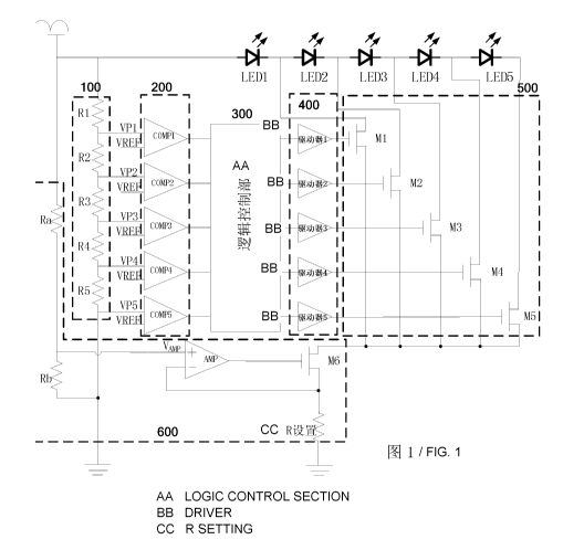
[0018] The main operation process of the LED lighting drive circuit of the
present invention is
CA 02918101 2016-01-12
that: when the supply voltage (a half sine wave from a commercial electric
supply through a
bridge rectifier) is zero, all of the power MOS tubes M1¨M5 are switched on.
As the supply
voltage gradually increases to reach the threshold voltage for turning on the
first group of
high-voltage LEDs, LED1 is turned on and the current flows to the ground
through the tube M1
and the tube M6. The voltage continues to increase, and when the voltage
reaches the threshold
voltage for turning on the second group of high-voltage LEDs, due to the
voltage dividing of the
resistors, the voltage at the terminal VP1 of the comparator COMP1 firstly
increases to be higher
than the constant reference voltage at its terminal VREF. The output voltage
level of the
comparator COMP1 jumps, through the logic control, to switch off the power MOS
tube Ml. At
this time, the power tubes M2, M3, M4 and M5 are remained as being switched
on, and the first
and second groups of high-voltage LEDs LED1 and LED2 are turned on. As the
voltage
continues to increase, and when the voltage reaches the threshold voltage for
turning on the third
group of high-voltage LEDs, due to the voltage dividing of the resistors, the
voltage at the
terminal VP2 of the comparator COMP2 increases to be higher than the constant
reference
voltage at its terminal VREF. The output voltage of the comparator COMP2
jumps, through the
logic control, to switch off the power MOS tube M2. At this time, the power
tubes M3, M4 and
M5 are remained as being switched on, and the first, second and third groups
of high-voltage
LEDs LED1, LED2 and LED3 are turned on. And so on, the voltage continues to
increase, and
the comparators COMP3 and COMP4 successively give a response to, through the
logic control,
successively switch off the MOS tubes M3 and M4, and then the third, fourth
and fifth groups of
high-voltage LEDs are successively turned on. Afterwards, the voltage starts
to decrease, the
power tubes M4, M3, M2 and M1 are successively switched on again, and the high-
voltage LED
groups are successively turned off, and such cycle repeats. Since the
variation frequency of
6
CA 02918101 2016-01-12
voltage is faster than the recognition frequency of human eyes, flickering
cannot be observed in
the whole process. Moreover, with the increase and decrease of the voltage,
the power tube M5
is always in a switch-on state.
[0019] It can be seen from the above operation of the circuit that, no voltage
transformer is
employed in the circuit. With the variation of the voltage, the high voltage
LEDs are
successively turned on, then successively turned off, and such cycle repeats.
Since the variation
frequency of the voltage is sufficiently faster than the recognition frequency
of human eyes, and
the effective value of the current is kept constant during the process, the
whole LED matrix emits
uniform and stable lights.
BRIEF DESCRIPTION OF THE DRAWINGS
[0020] Fig.1 is a circuit diagram of an LED lighting drive circuit according
to the present
invention;
[0021] Fig.2 is a preferred circuit diagram of a comparator in the LED
lighting drive circuit
according to the present invention;
[0022] Fig.3 is a preferred circuit diagram of a logic control section in the
LED lighting drive
circuit according to the present invention; and
[0023] Fig.4 is a graph of simulation current and voltage profiles of the LED
lighting drive
circuit according to the present invention.
DETAILED DESCRIPTION OF THE INVENTION
[0024] In order to make objectives, technical solutions and advantages of the
present invention
more apparent, hereinafter, the present invention will be further described in
detail with
7
CA 02918101 2016-01-12
reference to specific embodiments and accompanying drawings. It should be
understood that, the
description are merely illustrative, and by no means limiting the scope of the
present invention.
In addition, in the following, description of well-known structures and
techniques will be omitted
to avoid obscuration of the idea of the present invention.
[0025] Fig.1 is a circuit diagram of an LED lighting drive circuit according
to the present
invention.
[0026] The LED lighting drive circuit of the present invention is configured
to supply power to
N groups of LED loads, and therefore includes N current paths (N is an integer
no less than 2).
The power supply to the entire circuit is of a half sine wave from a
commercial electric supply
through a bridge rectifier. In a preferred embodiment of the present
invention, there are 5 groups
of loads for example. However, the present invention is not limited thereto,
and any N of groups
of LED loads can be applied to the LED lighting drive circuit of the present
invention, as long as
the number of current paths is increased according to a similar principle.
[0027] As shown in Fig. 1, the LED lighting drive circuit includes N current
paths and a constant
current section 600. The N current paths respectively drive N groups of LED
loads to emit lights.
Each current path includes successively: a voltage dividing section 100, a
comparator section
200, a logic control section 300, a power drive section 400 and a switch
section 500.
[0028] The voltage dividing section 100 is connected to a power supply, and
configured to
reduce the voltage of the power supply to a voltage available for a
corresponding current path.
As shown in Fig. 1, the voltage dividing section 100 includes N voltage
dividing resistors, for
example RI¨RS. These resistors are successively connected in series. Wherein
the voltage
dividing resistor R1 for a first path has a terminal connected to the power
supply, and has a
resistance much larger than the voltage dividing resistors R2¨R5 for other
paths. The voltage
8
CA 02918101 2016-01-12
dividing resistor R5 for an Nth path has a terminal connected to the ground.
Except for the
terminal of R1 which is connected to the power supply, a voltage dividing
resistor Ri for an ith
current path is connected to both of a positive terminal of a comparator COMPi
of the
corresponding path and a positive terminal of a comparator COMPi-1 of the
previous path,
where i=2, 3, 4, ..., N. In the embodiment of Fig. 1, terminals of the
resistors R2¨R5 are
respectively and successively connected to the positive terminals of the
comparators COMP1,
COMP2, COMP3, COMP4 and COMPS.
[0029] The comparator section 200 has an input terminal connected to an output
terminal of the
voltage dividing section 100, and is configured to output a corresponding
control signal to the
logic control section 300 when the voltage varies, to control the switch
section 500 to be
switched on and off, and in turn, to control LEDs in the paths to be turned on
and off. As shown
in Fig. 1, the comparator section 200 includes N comparators, for example
COMP1¨COMP5.
These comparators respectively belong to a current path of one of the LED
loads. Each of the
comparators has a positive terminal connected to a negative terminal of a
voltage dividing
resistor of the corresponding current path. Each of the comparators has a
negative terminal
connected to a constant reference voltage VREF. Optionally, the reference
voltage VREF can be
supplied by other power supply module with a constant voltage which satisfies
the input scope of
the comparator, to ensure normal operation of the comparator.
[0030] Operation principle of the comparator section 200 is as follows. The
voltage of the power
supply varies. Due to the presence of the voltage dividing resistors, when the
voltage increases,
voltages (for example, VP1, VP2, VP3 and VP4) at the positive terminals of the
comparators
successively increase, until they are higher than the reference voltage VREF
at the negative
terminals of the comparators. The comparators COMP1, COMP2, COMP3 and COMP4
9
CA 02918101 2016-01-12
successively output high voltage levels to the logic control section LOGIC
300, in turn, to
control power MOS tubes Ml, M2, M3 and M4 in the switch section 500 to be
successively
switched off, such that LED strings of a successively increased number are
turned on. When the
voltage decreases, voltages at positive terminals of comparators successively
decrease, until they
are lower than the reference voltage VREF at the negative terminals of the
comparators. The
comparators COMP1, COMP2, COMP3 and COMP4 successively output low voltage
levels to
the logic control section LOGIC 300, in turn, to control the power MOS tubes
Ml, M2, M3 and
M4 to be successively switched on, such that LED strings of a successively
decreased number
are turned on. In addition, a last comparator COMPN (for example the
comparator COMPS) of
the Nth current path has the positive terminal VP5 connected to the ground,
and its output is
maintained at a low voltage level, such that the power MOS tube M5 of this
path can be
maintained as switched on. When each of the MOS tubes MN (N<S) is switched
off, LED in the
path corresponding to M5 is turned on; and when any one of the MOS tubes MN
(N<S) is
switched on, the LED in the path corresponding to MS is turned off.
[0031] Fig.2 is a preferred circuit diagram of a comparator in the LED
lighting drive circuit
according to the present invention.
[0032] As shown in Fig. 2, a preferred comparator in the present invention can
consist of two
stages of operational amplifiers and inverters, wherein a first stage of the
two stages of
operational amplifiers is of a differential input single-terminal output
structure, signals outputted
from the operational amplifiers are outputted as logic signals after rectified
by the inverters. The
two stages of amplifiers amplify a difference between an input signal IN+ and
an input signal IN-,
and the amplified signal is rectified by the inverters to be output as a logic
signal.
[0033] The logic control section 300 is connected to an output terminal of the
comparator section
CA 02918101 2016-01-12
,
200 and includes a plurality of NOR gates and a plurality of inverters for
controlling the
successive turning on and off of the switch section 500 during the variation
of the voltage.
[0034] Fig.3 is a preferred circuit diagram of a logic control section in the
LED lighting drive
circuit according to the present invention.
[0035] As shown in Fig. 3, the logic control section 300 includes NOR gates
201-204 and
inverters 101-109. In addition, the logic control section 300 includes enable
terminals El, E2,
E3, E4 and E5. Each of the enable terminals outputs a high voltage level or a
low voltage level
depending on the variation of the voltage. After being driven by power tube
drivers 1-5, the
outputs respectively control the power MOS tubes to be switched on or off, and
in turn, to
control the LED loads in the current paths to be turned on or off.
[0036] The NOR gate 201 in the first current path has an input terminal
connected to the output
terminal of the comparator COPM1 and another input terminal connected to an
input terminal of
the inverter 102 and an output terminal of the inverter 101 in the next
current path (i.e. the
second current path). The NOR gate 201 has an output terminal connected to the
power tube
driver 1 in the corresponding current path (i.e. the first current path).
[0037] The NOR gate 202 in the second current path has an input terminal
connected to the
output terminal of the comparator COPM2 and another input terminal connected
to an input
terminal of the inverter 104 and an output terminal of the inverter 103 in the
next current path
(i.e. the third current path). The NOR gate 202 has an output terminal
connected to the first
inverter 101 in the corresponding current path (i.e. the second current path).
The second inverter
102 is connected to the power tube driver 2 in the corresponding current path.
[0038] The NOR gate 203 in the third current path has an input terminal
connected to the output
terminal of the comparator COPM3 and another input terminal connected to an
input terminal of
11
CA 02918101 2016-01-12
the inverter 106 and an output terminal of the inverter 105 in the next
current path (i.e. the fourth
current path). The NOR gate 203 has an output terminal connected to the first
inverter 103 in the
corresponding current path (i.e. the third current path). The second inverter
104 is connected to
the power tube driver 3 in the corresponding current path.
[0039] The NOR gate 204 in the fourth current path has an input terminal
connected to the
output terminal of the comparator COPM4 and another input terminal connected
to an input
terminal of the inverter 109 and an output terminal of the inverter 108 in the
next current path
(i.e. the fifth current path). The NOR gate 204 has an output terminal
connected to the power
tube driver 4 in the corresponding path (i.e. the fourth current path) via the
first inverter 105 and
the second inverter 106 in the fourth current path.
[0040] The logic control section of the Nth current path (i.e. the fifth
current path) includes three
inverters 107,108 and 109, wherein the first inverter 107 has an input
terminal connected to the
output terminal of the comparator COMPS, and an output terminal connected to
the power tube
driver 5 in the corresponding path (i.e. the fifth current path) via the
second inverter 108 and the
third inverter 109.
[0041] The power drive section 400 is connected to the output terminal of the
logic control
section 300, and configured to provide a gate voltage required by turning on
and off a power
MOS tube. As shown in Fig. 1, the power drive section 400 includes a plurality
of power tube
drivers, for example, drivers 1-5, respectively disposed in the first to fifth
current paths. Each of
the drivers 1-5 has an output terminal connected to a gate electrode of a
power MOS tube
(M 1¨M5) in the corresponding current path, to control the power MOS tube to
be turned on and
off according to the output signal of the enable terminal of the logic control
section 300.
[0042] The switch section 500 has an input control terminal connected to an
output terminal of
12
CA 02918101 2016-01-12
the power drive section 400, and is configured to control the LED loads to be
turned on and off
As shown in Fig. 1, the switch section 500 includes a plurality of power MOS
tubes, for example
M 1 ¨M5, respectively disposed in the first to fifth current paths. Each of
the power MOS tubes
has a gate electrode connected to the output terminal of the power tube driver
in the
corresponding current path, a drain electrode connected to the LED load in the
corresponding
current path and a source electrode connected to a drain of the MOS tube M6 in
the constant
current section 600. When each of the power MOS tubes is switched on, the LED
load in the
corresponding current path is turned off When the power MOS tubes are
successively switched
off, the LED loads in the corresponding current paths are successively turned
on. In the present
invention, the power MOS tubes M 1 ¨M5 are preferably high-voltage power tubes
which can
endure a voltage higher than the maximum threshold of all of the LED loads.
[0043] The LED lighting drive circuit of the present invention also includes
the constant current
section 600, configured to provide a constant current for the drive circuit.
As shown in Fig. 1, the
constant current section 600 includes voltage dividing resistors Ra and Rb, an
error amplifier
AMP, a MOS M6 and a sampling resistor Rset., wherein the resistor Ra has a
terminal connected
to the power supply (a half sine wave from a commercial electric supply
through a bridge
rectifier) and another terminal connected to a terminal of Rb and a positive
input terminal of the
error amplifier AMP. Another terminal of Rb is connected to the reference
ground. The error
amplifier AMP has a negative input terminal connected to a source electrode of
the MOS tube
M6 and a terminal of the sampling resistor Rset, and an output terminal
connected to a gate
electrode input terminal of the MOS tube M6. Another terminal of the sampling
resistor Rset is
connected to the reference ground. A drain electrode of the MOS tube M6 as an
output terminal
is connected to the switch section 500. The voltage dividing resistors Ra and
Rb are configured
13
CA 02918101 2016-01-12
to divide the sine-waved supply voltage to a voltage appropriate for the
operation of the error
amplifier AMP, and the voltage resulted from the dividing varies in a half
sine wave form with
the supply voltage. When the current is in a normal operation, the error
amplifier has its positive
input voltage equal to its negative input voltage, then a current passing
through the sampling
resistor Rset is VAmPaset. As the supply voltage varies, a current passing
through the LEDs varies
accordingly. Through the constant current section 600, the current passing
through the LED
strings varies in a half sine wave form with the input AC power supply and is
maintained at a
constant effective value. The effective value of the current can be adjusted
through the resistor
Rset
[0044] Hereinafter, the operation principle of the LED lighting drive circuit
of the present
invention will be described with reference to Figs. 1 to 3.
[0045] The supply voltage is a half sine wave from a commercial electric
supply through a
bridge rectifier. When the supply voltage is 0, each of the comparators COMP1¨
COMPS
outputs "0". Through the NOR gates and the inverters in the logic control
section 300, each of
the enable terminals El, E2, E3, E4 and E5 of the logic control section 300
outputs a high
voltage level "1". Through the driving of the power tube drivers 1-5, each of
the power MOS
tubes M1¨M5 is controlled to be switched on. However, since the supply voltage
is 0, less than
the threshold voltage for turning on the LED lights, so the LED strings are
turned off. With the
increase of the supply voltage, the light string LED1 is firstly turned on.
[0046] With the further increase of the supply voltage, due to the
characteristic of LED devices,
the light string LED1 will maintain its voltage. When the supply voltage
reaches the threshold
voltage for turning on both of the LED lights LED1 and LED2, with set
resistances of the
resistors in the voltage dividing section 100, a voltage VP1 at the positive
terminal of the
14
CA 02918101 2016-01-12
comparator COMP1 can firstly increase to be higher than the reference voltage
VREF at its
negative terminal. The comparator COMP1 outputs a high voltage level "1",
through the NOR
gate 201, then the enable terminal El in the corresponding current path
outputs a low voltage
level "0". After the driving of the power tube driver 1, the power MOS tube M1
is controlled to
be switched off. At this time, the power MOS tube M2, M3, M4 and M5 are
maintained as being
switched on and the high-voltage groups of LEDs LED1 and LED2 are turned on to
emit light.
The current through the LEDs flows to the ground through M2, M6 and Rset. The
instantaneous
current is:
= VAMP
Rset
[0047] Where VAmp is the instantaneous voltage at the positive terminal of the
error amplifier
AMP.
[0048] Afterwards, the supply voltage continues to increase to the threshold
voltage for turning
on LED1, LED2 and LED3. Due to the voltage dividing of the resistors, the
voltage at the
terminal VP2 of the comparator COMP2 increases to be higher than the reference
voltage VREF
at its negative terminal. The output of the comparator COMP2 jumps to "1",
through the NOR
gate 202 and the inverters 101 and 102, the enable terminal E2 outputs "0", to
switch off the
power MOS tube M2. The power tubes M3, M4 and M5 are maintained as being
switched on. At
this time, the high-voltage groups of LEDs LED1, LED2 and LED3 are turned on.
The current
through the LEDs flows to the ground through M3, M6 and Rset. The
instantaneous current is:
V
= AMP
Rset
[0049] Where VAMP is the instantaneous voltage at the positive terminal of the
error amplifier
AMP.
CA 02918101 2016-01-12
[0050] Afterwards, the supply voltage continues to increase, the enable
terminals E3 and E4 in
the other current paths successively output a low voltage level, to
successively switch off the
MOS tubes M3 and M4 and successively turn on LED4 and LEDS.
[0051] When the supply voltage reaches a maximum value (a peak value of a half
sine wave)
and then starts to decrease, the enable terminals E4, E3, E2 and El
successively outputs a high
voltage level to successively switch on the power MOS tubes M4, M3, M2 and Ml,
such that the
number of LED strings being turned on is successively decreased, and such
cycle repeats.
[0052] In addition, during the whole process of the variation of the supply
voltage, the enable
terminal E5 in the last path (i.e. the fifth current path) is maintained at a
high voltage level such
that the MOS tube M5 is maintained as being switched on. When each of the MOS
tubes MN
(N<5) is switched off, LED in the path corresponding to M5 is turned on; and
when any one of
the MOS tubes MN (N<5) is switched on, the LED in the path corresponding to M5
is turned off
[0053] Since the variation frequency of the voltage is faster than the
recognition frequency of
human eyes, flickering cannot be observed in the whole process. Moreover, with
the increase and
decrease of the voltage, the power tube M5 is always in a switch-on state.
[0054] It can be seen from the above operation principle that, no voltage
transformer is
employed in the circuit. With the variation of the voltage, the high voltage
LEDs are
successively turned on, then successively turned off, and such cycle repeats.
Since the variation
frequency of the voltage is sufficiently faster than the recognition frequency
of human eyes, and
the effective value of the current is kept constant during the process, the
whole LED matrix emits
uniform and stable lights.
[0055] Fig.4 is a graph of simulation current and voltage profiles of the LED
lighting drive
circuit according to the present invention. As shown in Fig. 4, the voltage is
a 220V AC wave
16
CA 02918101 2016-01-12
which is full-wave rectified with a peak value of 310V. When the voltage
reaches the threshold
of the first group of LEDs, a current will occur on the LEDs. Afterwards, the
wave of the current
varies in a half sine wave form with the supply voltage with a frequency of
100Hz. Since the
effective value of the current is kept constant during the process, it can
ensure that the LED
matrix emits uniform and stable lights. Moreover, since the input current and
voltage of the
circuit are in a half sine wave form and vary simultaneously, the circuit can
achieve a desirable
power factor.
[0056] It should be understood that, the above specific embodiments of the
present invention are
merely for illustration or explanation of the present invention, and do not
constitute restrictions.
Therefore, modifications, equivalent replacements, improvements and the like
may be made.
17