Note: Descriptions are shown in the official language in which they were submitted.
1
CONTROL ARRANGEMENT FOR INCREASING THE
AVAILABLE OUTPUT FROM A SOURCE
This invention relates to a control arrangement, and in particular to a
control arrangement
suitable for use with a photovoltaic or solar panel (referred to hereinafter
as a solar panel)
to increase the available output therefrom. Whilst
especially suitable for use in
conjunction with a solar panel, the control arrangement may be used with a
range of other
devices or power supplies.
Solar panels are in increasingly widespread use in the generation of
electricity. The
outputs therefrom may be used directly in driving other devices, or may be
used in
charging electrical storage means or in supplying power to the mains
electricity network.
As the output of a solar panel varies, non-linearly, depending upon, for
example, the
intensity of the light incident thereon, the operating temperature, and other
factors, the
direct, uncontrolled supply of the output from the solar panel to a load is
usually
inappropriate. Figure 1 illustrates, diagrammatically, a typical I-V output of
a solar panel
under a range of incident light intensities, showing the relationship between
the generated
current and the associated output voltage. The maximum power output occurs if
the
circuit, of which the solar panel forms part, is operating on the line 10 in
Figure 1. Clearly,
as the light intensity changes, the operating current and voltage required for
the maximum
output vary. In order to ensure that the solar panel and associated circuit
operate at
around the point of maximum power, a maximum power point tracking algorithm is
used.
The output of the maximum power point tracking algorithm is used in varying
the load
supplied by the solar panel, for example switching in or out resistances
thereof, in an
attempt to maintain the operation of the solar panel at around its optimum
point.
In some older systems the algorithm operates to ensure that the circuit
operates at 70% of
the open circuit voltage. This
is achieved by repeatedly and rapidly connecting
disconnecting the supply, ie the output from the solar panel, from the load.
By way of
example, the supply may be connected and disconnected in the region of 1000 to
3000
Date Recue/Date Received 2021-03-17
CA 02918184 2016-01-13
WO 2015/008035 PCT/GB2014/052104
2
times per second. By disconnecting the output for a proportion of the time in
this manner,
the duty cycle is reduced, for example to around 70% as mentioned above.
Whilst such a system may operate satisfactorily in some circumstances, when
the supply
is disconnected there is no output from the panel to the load and
consequently, even if the
panel would otherwise be operating at the maximum power point, potential power
is being
lost whilst the panel is disconnected. The arrangement is therefore less
efficient than it
could be.
It is an object of the invention to provide a control arrangement whereby the
useful output
of a panel can be enhanced and, preferably optimised.
According to the present invention there is provided a control arrangement for
use in
controlling the electrical supply from a power supply unit including an
internal capacitance
to an output, the control arrangement comprising an inductor, a switch
arranged in parallel
with internal capacitance, and a controller operable to control the operation
of the switch
such that closing of the switch results in the formation of an LCR circuit,
the internal
capacitance forming the capacitance of the LCR circuit.
In such an arrangement there is no need to provide a maximum power point
tracking
algorithm or the like, and preferably no such algorithm or the like is
present.
A pn junction diode, by its nature, forms a variable junction capacitance.
Such a diode is
typically present in a unit including a solar panel. This junction capacitance
has, in the
past, been ignored when modeling the output of a solar panel and associated
control
circuit. Where such a diode is arranged in parallel with a voltage source such
as a solar
panel, part of the supply is used, initially, in charging the junction
capacitance.
CA 02918184 2016-01-13
WO 2015/008035 PCT/GB2014/052104
3
Furthermore, where the voltage source takes the form of a solar panel, the
source itself
will in effect form a capacitance which will also become charged. As the
output of a solar
panel is not uniform but varies with, for example, incident light intensity,
temperature and
other factors, the charge on the capacitance(s) is constantly varying. The
capacitor
current associated with the internal capacitance can thus either be positive
or negative
depending upon whether, at any given point in time, the capacitance is being
charged or is
discharging. In a conventionally arranged solar panel, the direction of this
current will
depend upon, for example, whether the intensity of the illumination is
increasing or
decreasing. However, in the arrangement outlined hereinbefore, extraction of
the internal
capacitance energy is achieved through the operation of the switch in a
controlled manner,
thereby allowing the operation of the overall system with an enhanced level of
efficiency.
In the arrangement of the invention, when the switch is open, the internal
capacitance of
the unit will charge. Closing of the switch will result in discharge of the
internal
capacitance into the inductor. By appropriate control over the operation of
the switch it will
be appreciated that the output from the power supply unit which would
otherwise just go
towards charging of the internal capacitance can instead be extracted for use.
When the
switch is opened again, resulting in the internal capacitance recharging,
energy can be
extracted from the inductor and used to satisfy the demands of a load
connected thereto.
Furthermore, when the switch is closed, the output current from the power
supply unit
flows through the inductance resulting in energy storage therein. When the
switch is
opened, power is supplied to the load. As long as the output current from the
power
supply is supplied continuously to the inductance, and the inductor current
rises upon
closing of the switch and decreased upon opening of the switch, the output
voltage from
the control arrangement will be greater than then input voltage thereto.
Preferably, the controller causes the switch to move between its opened and
closed
positions at a frequency in the range of 150-700kHz, preferably 600-700kHz,
for example
at a frequency of the order of 650kHz. Variation of the size of the inductance
changes the
frequency at which the switch should be operated.
CA 02918184 2016-01-13
WO 2015/008035 PCT/GB2014/052104
4
Where the power supply unit includes an inverter, such as a string inverter or
a
microinverter used in conjunction with a solar panel, the control arrangement
may be
incorporated into the inverter or may comprise a module adapted for connection
thereto.
The invention further relates to a method for controlling the output of unit
using a control
arrangement of the form outlined hereinbefore, the method comprising the steps
of:
opening the switch, thereby allowing the internal capacitance of the unit to
become
charged;
closing the switch, thereby allowing the internal capacitance of the unit to
discharge, supplying an increased current to the inductor; and
re-opening the switch, thereby allowing the internal capacitance of the unit
to
become recharged whilst extracting energy from the inductor to satisfy the
electrical
demand of a load.
The invention will further be described, by way of example, with reference to
the
accompanying drawings, in which:
Figure 1 is a diagram illustrating the I-V output relationship for a typical
solar panel unit
under a range of incident light intensities;
Figure 2 is a diagram illustrating a control arrangement according to an
embodiment of the
invention;
CA 02918184 2016-01-13
WO 2015/008035 PCT/GB2014/052104
Figure 3 is a graph comparing the output of the control arrangement of Figure
2 with a
conventional solar panel control arrangement; and
Figure 4 is a diagram illustrating an alternative embodiment.
5
As illustrated in Figure 1 and discussed hereinbefore, the output of solar
panels varies
significantly depending upon a number of factors, not least of which is the
intensity of the
light incident upon the solar panel as any given time.
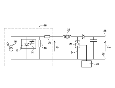
Referring to Figure 2, a circuit diagram of a control arrangement in
accordance with an
embodiment is illustrated. The circuit diagram is representative of a control
arrangement
used in controlling the output from a solar panel in order to allow the
maximum power to
be extracted therefrom. Whilst described in connection with a solar panel, it
will be
appreciated that the invention may be used in other applications in which it
is desired to
enhance the level of power that can be extracted from a unit including a
variable voltage
source and an internal capacitance.
As shown in Figure 2, a solar panel 10 has, connected across the terminals
thereof, a pn
junction diode 12. Such a diode 12 has an internal, junction capacitance
illustrated in
Figure 2 by the capacitance 14. Whilst not illustrated, the solar panel 10
will also have a
diffusion capacitance associated therewith. The panel 10 and diode 12 are
typically
supplied as a single unit, denoted by dashed lines 16 in Figure 2, with
constant
resistances 18, 20 reflecting resistances present within the unit 16, and with
the junction
capacitance 14 and diffusion capacitance constituting a variable internal
capacitance of
the unit 16. Vp thus represents the voltage output from the unit 16. It will
be appreciated
that this output is variable for the reasons discussed hereinbefore.
CA 02918184 2016-01-13
WO 2015/008035 PCT/GB2014/052104
6
The output from the unit 16 is supplied to an inductor 22, a line 24 including
a switch 26
being provided and arranged such that when the switch is open, the output of
the panel 10
serves to charge the internal capacitance of the unit 16 and also serves to
satisfy the
requirements of a load connected to output terminals 28. Vopt represents the
output
voltage from the control arrangement. The inductance of the inductor 22 is
preferably
relatively small, being selected to match the characteristics of the solar
panel 10 and the
internal capacitance thereof.
When the switch 26 is closed, the internal capacitance of the unit 16 is able
to discharge,
the closing of the switch 26 in the line 24 resulting in the formation of an
LCR circuit, the
discharge from the internal capacitance being supplied to the inductor 22,
increasing the
current supply thereto such that upon subsequent reopening of the switch 26,
energy from
the inductor 22 can be extracted and used in satisfying the load. When the
switch 26 is
closed the increased output current from the unit 16 is supplied to the
inductance 22,
resulting in energy storage therein. Subsequent opening of the switch allows
power to be
extracted from the inductance 22 and supplied to the load whilst also
resulting, once more,
in charging of the internal capacitance. Provided the output current from the
unit 16 is
supplied continuously to the inductance 22 and the inductor current rises when
the switch
26 is closed and falls when the switch 26 is opened (and the control unit 30
mentioned
below is operated in such a manner as to ensure that the is the case) then the
value of
Vapt will be greater than V. Figure 3 demonstrates this, the outputs (in Volt-
Amperes) of a
conventionally controlled panel (horizontal axis) and a panel controlled using
the
aforementioned control arrangement (vertical axis) under the same
environmental
conditions, the panels having the same operating characteristics other than in
relation to
the control thereof, being plotted against one another and clearly showing
that the Võt is
greater, often significantly greater, than Vp.
The frequency of operation of the switch 26 is chosen so as to maintain this
effect. The
frequency may thus be chosen to maintain resonance, or may be a harmonic of a
frequency that would maintain resonance. As the internal capacitance of the
unit 16 is not
fixed, it will be appreciated that the optimum switching frequency is also not
fixed.
CA 02918184 2016-01-13
WO 2015/008035 PCT/GB2014/052104
7
However, it will typically be in the region of 150 to 700 kHz, preferably
600kHz to 700kHz.
The optimum switching frequency will depend, at least to some degree, upon the
size of
the inductance.
The operation of the switch 26 is controlled by an appropriate controller 30
which serves to
controlling the timing and frequency of operation of the switch 26. As
mentioned
hereinbefore, to some degree the frequency of operation of the switch 26
should be varied
to compensate for variations in the internal capacitance of the unit 16.
However, it is
anticipated that the variation in frequency required to take into account such
variations will
be fairly small and that the variations in the switching frequency will
typically be in the
region of 50-60Hz. The controller 30 conveniently monitors, for example, the
output Vp
from the unit 16, uses this to provide an indication of the internal
capacitance of the unit 16
at that time, and controls the switching frequency in response to this in
order to maximize
or substantially maximize the power output. However, it will be appreciated
that other
techniques to determine the optimum, or a desirable, switching frequency are
possible
without departing from the scope of the invention.
The use of the control arrangement outlined hereinbefore is advantageous in
that is allow
the useful output of the solar panel unit 16 to be enhanced whilst avoiding
the need to
employ a complex maximum power point tracking algorithm, and avoiding the
inefficiencies associated therewith. The control arrangement is preferably
located close to
the unit 16 to minimize the effects of inductances associated with the
connecting cables.
It could, for example, be incorporated into an inverter such as a string
inverter or
microinverter associated with the unit 16, or as a module to be connected
thereto.
Turning to Figure 4, and alternative circuit configuration is illustrated. In
the arrangement
of Figure 4, rather than provide a single inductance 22, a pair of inductances
22a, 22b are
provided in respective legs of the circuit, each inductance 22a, 22b having a
respective
CA 02918184 2016-01-13
WO 2015/008035 PCT/GB2014/052104
8
switch 26a, 26b associated therewith, the operation of the switches 26a, 26b
being
controlled by a controller 30 as described hereinbefore.
Each inductance 22a, 22b forms the input coil of a respective bifilar inductor
32a, 32b, the
.. output coils 34a, 34b being connected to and supplying the output voltage
to the load, in
use. The input and output coils of each bifilar inductor 32a, 32b share a
common core and
so are magnetically coupled to one another. Blocking diodes 36a, 36b are
provided to
prevent the bifilar inductors 32a, 32b acting as transformers. In use, when
switch 26a is
closed, the internal capacitance 14 discharges and increases the current
supply to the
.. inductance 22a resulting in energy storage therein. Subsequent opening of
the switch 26a
results in the internal capacitance 14 charging and in energy discharge from
the
inductance 22a in the manner outlined hereinbefore. Whilst energy is being
discharged
from the inductance 22a, switch 26b can be closed to discharge the internal
capacitance
14 increasing the current supply to the inductance 22b, subsequent opening of
the switch
.. 26b again allowing the internal capacitance 14 to charge and in energy
discharge from the
inductance 22b to the load.
Accordingly, starting from a position in which both switches 26a, 26b are
open, and so the
internal capacitance 14 is charging, at a selected point in time the switch
26a is closed
.. resulting in discharge of the internal capacitance 14. Switch 26a is then
opened to
recharge the capacitance and commence discharge the inductor 22a. Switch 26b
is then
closed to discharge the internal capacitance 14 and is then reopened to
recharge the
capacitance 14 and commence energy discharge from the inductor 22b. Before
reopening
each switch 26a, 26b, it may be beneficial to include a period during which
both switches
.. 26a, 26b are closed. The timings at which the commencement of each charging
and
discharging cycle of the unit 16 occurs will depend, in part, upon the
prevailing
environmental conditions, thus the switching frequency will not normally be
fixed if the
efficiency of the control arrangement is to be maximized. An appropriate
control algorithm
may be used to control the times at which the switches 26a, 26b are opened and
closed,
.. for example to maximize the output. The algorithm may be controlled
depending upon the
output voltage from the panel 16, for example.
CA 02918184 2016-01-13
WO 2015/008035 PCT/GB2014/052104
9
It will be appreciated that by appropriate control over the times at which the
switches 26a,
26b are moved between their open and closed positions, the output of the
control
arrangement may be optimized.
The capacitance 38 and diode 40 are provided to reduce the back EMF from the
inductors
32a, 32b charging the unit 16. The capacitance 38 is smaller than the internal
capacitance of the unit 16.
It is thought that the use of the invention may allow greater flexibility over
the location and
orientation in which units 16 may be employed as the use of the invention may
allow a
useful output to be generated in situations in which no such useful output
would otherwise
be produced. Useful generation under reduced intensity lighting conditions (or
with units
not orientated optimally) or under unfavourable temperature conditions may be
possible.
Whilst specific embodiments of the invention are described hereinbefore, it
will be
appreciated that a number of modifications and alterations to the arrangement
may be
made without departing from the scope of the invention.