Note: Descriptions are shown in the official language in which they were submitted.
ELECTRON SOURCE, X-RAY SOURCE AND DEVICE USING THE X-RAY
SOURCE
FIELD OF THE INVENTION
[01] The present disclosure relates to an electron source for generating
electron beam
currents and an X-ray source for generating X-rays by using the electron
source, particularly
to an electron source for generating electron beam currents from different
locations in a
predetermined manner, an X-ray source for generating X-rays from different
locations in a
predetermined manner and a device using the X-ray source.
BACKGROUND
[02] An electron source is a device or component capable of generating
electron beam
currents, often called electron gun, cathode, emitter, etc. Electron sources
are widely used in
displays, X-ray sources, microwave tubes, etc. An X-ray source is a device
that generates X-
ray. The core part of the X-ray source is an X-ray tube. The X-ray source
comprises an
electron source, an anode and a vacuum seal housing, and usually further
comprising a power
supply, a control system and auxiliary components, such as a cooling, a shield
and so on. The
X-ray source is widely used in industrial nondestructive testing, security
check, medical
diagnosis and treatment, etc.
[03] Traditionally, an X-ray source adopts a direct cooling tungsten filament
as the
cathode. During operation, the filament through which an electric current
flows is heated to an
operating temperature of about 2000K and then generates an electron beam
current through
thermal emission. The electron beam current is accelerated by an electric
field at hundreds of
thousands of voltage between the anode and the cathode toward the anode,
strikes a target and
then generates an X-ray.
[04] Field emission can be caused by a plurality of materials, such as metal
needle,
carbon nano-tube, etc., to emit electrons at room temperature and generate
electron beam
currents. After the development of nanotechnology, especially carbon nano-
material, field
emission electron sources with nano-materials grow quickly.
CA 2919744 2017-06-08
[05] An X-ray source requires its electron source to have a large emission
current,
usually larger than lmA. For example, in existing medical CTs, oil-cooled X-
ray sources with
rotating targets can emit an electric current of up to 1300mA. As disclosed in
Patent
Reference 1, in an existing X-ray device which adopts a field emission
electron source with
nano-material as cathode, in order to obtain a large emission electric
current, a cathode
emission surface with a macro size is formed from nano-material, and a mesh
grid is arranged
above and in parallel with the emission surface to control the field emission.
In such structure,
due to machining accuracy, deformation of the mesh and installation accuracy,
there is a large
distance between the mesh grid and the cathode surface, thus the grid needs a
very high
voltage, normally larger than 1000V, to control the field emission.
[06] Usually, electron emission units using the field emission principle have
the
substantially same structure, for example, as shown in parts (A), (B) and (C)
of FIG. 3. Part
(A) of FIG. 3 shows the technical solution disclosed in Patent Reference 2,
wherein a nano-
material 31 is adhered to a structure 13 of a substrate 10. Part (B) of FIG. 3
shows the
technical solution disclosed in Patent Reference 3, wherein a nano-material 20
is directly
formed on flat surfaces of substrates 12 and 14. Part (C) of FIG. 3 shows the
technical
solution disclosed in Patent Reference 4, wherein an electron source for an X-
ray source
device comprises a nano-material surface 330 with a micro size (millimeters to
centimeters),
and its grid is a mesh grid with a micro size, and the grid surface is
parallel to the nano-
material surface.
Patent Reference 1: CN102870189B;
Patent Reference 2: US5773921;
Patent Reference 3: US5973444; and
Patent Reference 4: CN100459019.
SUMMARY OF THE INVENTION
[07] An aspect of the present invention provides a field emission electron
source that
has a novel structure, for purpose of achieving simple structure, low cost,
low control voltage
and large intensity of emission current. It is also provided an X-ray source
using the electron
source, which has a large output intensity of X-ray and a low cost, or getting
a number of X-
2
CA 2919744 2017-06-08
ray target spots at different positions, wherein the target spot have a large
beam intensity and
a small gap.
[08] An aspect of the present invention provides a field emission electron
source that
has a low control voltage and a large emission current and an X-ray source
using the electron
source. The electron source of the present invention comprises at least two
electron emission
zones, each of which comprises a plurality of micro electron emission units.
The structure of
the micro electron emission unit in the present invention enables a very low
control voltage
for field emission. The combined operation of numerous electron emission units
provides the
electron emission zone with a large emission current. The X-ray source using
the electron
source may be designed as a dual-energy X-ray source by means of the design
for the anode.
Through the design for the electron source, a distributed X-ray source with a
plurality of
target spots at different locations can be achieved. Multiple operation modes
can improve an
output intensity of X-ray at each target spot, reduce gaps between the
targets, avoid black
spots, and extend functions and applications of the distributed X-ray source
for field emission.
Moreover, by reducing control voltage, it is possible to facilitate control of
the system and
reduce production cost and malfunction, thereby extending life of the
distributed X-ray source.
[09] Furthermore, an aspect of the present invention further provides
applications of the
above distributed X-ray source into X-ray transmission imaging system and back
scattering
imaging system. Various technical solutions using the X-ray source show one or
more
advantages, including low cost, fast detection speed, high quality imaging,
etc.
[010] Furthermore, an aspect of the present invention further provides real-
time image-
guided radiotherapy system. Regarding therapy of body parts having
physiological
movements, for example lung, heart and so on, the "real-time" image-guided
radiotherapy can
decrease exposure doses and reduce exposure to normal organics, which is very
important.
Moreover, the distributed X-ray source of the present invention has a number
of target spots
and thus can obtain "three-dimensional" diagnostic images having depth
information, which
differ from normal planar images. In the image-guided radiotherapy, this can
further improve
the guiding accuracy and locating precision of the radiation beams for
radiotherapy.
[011] To achieve objects of the present invention, the following technical
solutions are
adopted.
3
CA 2919744 2017-06-08
[012] An aspect of the present invention provides an electron source,
comprising: at least
one electron emission zone, which comprises a plurality of micro electron
emission units,
wherein the micro electron emission unit comprises: a base layer, an
insulating layer on the
base layer, a grid layer on the insulating layer, an opening in the grid
layer, and an electron
emitter that is fixed at the base layer and corresponds to a position of the
opening, and
wherein all the micro electron emission units in the electron emission zone
simultaneously
emit electrons or do not emit electrons at the same time.
[013] Furthermore, in the present invention, the base layer may be used to
provide
structural support and electrical connection.
[0141 Furthermore, in the present invention, the grid layer may be made of
conductive
materials.
[015] Furthermore, in the present invention, the opening may penetrate through
the grid
layer and the insulating layer and reaches the base layer.
[016] Furthermore, in the present invention, the insulating layer may have a
thickness
less than 200 m.
[017] Furthermore, in the present invention, the opening may have a size that
is less than
the thickness of the insulating layer.
[018] Furthermore, in the present invention, the opening may have a size that
is less than
a distance from the electron emitter to the grid layer.
[019] Furthermore, in the present invention, the electron emitter may have a
height that
is less than half of a thickness of the insulating layer.
[020] Furthermore, in the present invention, the electron emitter may be
formed to
comprise nano-materials.
[021] Furthermore, in the present invention, the grid layer may be parallel to
the base
layer.
[022] Furthermore, in the present invention, the micro electron emission unit
may
occupy a spatial size at a micrometer level along an array arrangement
direction. Preferably,
the spatial size occupied by the micro electron emission unit along an array
arrangement
direction may be ranged from lp.m to 200 m.
4
CA 2919744 2017-06-08
[023] [Furthermore, in the present invention, a ratio of a length to a width
of the electron
emission zone may be larger than 2.
[024] Furthermore, in the present invention, the base layer may comprise a
substrate
layer and a conducting layer on the substrate layer, and the electron emitter
may be fixed at
the conducting layer.
[025] Furthermore, in the present invention, an emission current of each
electron
emission zone may be not smaller than 0.8mA.
[026] Furthermore, an aspect of the present invention provides an electron
source,
comprising: at least two electron emission zones, each of which comprises a
plurality of micro
electron emission units, wherein the micro electron emission unit comprises: a
base layer for
providing structural support and electrical connection, an insulating layer on
the base layer, a
grid layer on the insulating layer made of a conductive material, an opening
that penetrates
through the grid layer and the insulating layer and reaches the base layer,
and an electron
emitter fixed at the base layer within the opening, wherein all the micro
electron emission
units in the same electron emission zone are electrically connected, and
simultaneously emit
electrons or do not emit electrons at the same time, and wherein different
electron emission
zones are electrically partitioned.
[027] Furthermore, in the present invention, the insulating layer may have a
thickness
less than 200iam.
[028] Furthermore, in the present invention, the grid layer may be parallel to
the base
layer.
[029] Furthermore, in the present invention, different electron emission zones
are
electrically partitioned means that: the respective base layers of all the
electron emission
zones are separated from each other, or the respective grid layers of all the
electron emission
zones are separated from each other, or both the respective base layers and
grid layers of all
the electron emission zones are separated from each other.
[030] Furthermore, in the present invention, different electron emission zones
can be
controlled to emit electrons at a predetermined sequence, such as emitting
electrons
successively, at intervals, alternatively, partially at the same time, group
by group, or in other
emission ways.
CA 2919744 2017-06-08
L,
[031] Furthermore, in the present invention, the respective base layers of all
the micro
electron emission units in the same electron emission zone may be the same
substantive layer,
the respective grid layers of all the micro electron emission units may be the
same substantive
layer, and the respective insulating layers of all the micro electron emission
units may be the
same substantive layer.
[032] Furthermore, in the present invention, a size of the micro electron
emission unit in
the electron emission zone along an array arrangement direction can be in a
micrometer level.
[033] Furthermore, in the present invention, a spatial size occupied by the
micro electron
emission unit along an array arrangement direction may be ranged from 11.1m to
200 m.
[034] Furthermore, in the present invention, the opening may have a size that
is less than
the thickness of the insulating layer.
[035] Furthermore, in the present invention, the opening may have a size that
is less than
a distance from the electron emitter to the grid layer.
[036] Furthermore, in the present invention, the electron emitter may have a
height that
is less than half of a thickness of the insulating layer.
[037] Furthermore, in the present invention, a linear length of the electron
emitter may
be perpendicular to a surface of the base layer.
[038] Furthermore, in the present invention, the electron emitter may be
formed to
comprise nano-materials.
[039] Furthermore, in the present invention, the nano-materials may comprise
single-
walled carbon nano-tubes, double-walled carbon nano-tubes, multi-walled carbon
nano-tubes,
or any combination thereof.
[040] Furthermore, in the present invention, the base layer may comprise a
substrate
layer and a conducting layer on the substrate layer. The base layer may be
used to provide
structural support. The conducting layer may be used to form electrical
connection between
the respective base layers (fixed electrode of nano-materials) of all the
micro electron
emission units in the same electron emission zone.
[041] Furthermore, in the present invention, a ratio of a length to a width of
the electron
emission zone may be larger than 2.
6
CA 2919744 2017-06-08
[042] Furthermore, in the present invention, the respective electron emission
zones may
have a same size, and may be arranged along their short edges in a parallel,
aligned and
uniform manner.
[043] Furthermore, in the present invention, an emission current of each
electron
=
emission zone may be larger than 0.8mA.
[044] Furthermore, an aspect of the present invention provides an X-ray
source,
comprising: a vacuum chamber; an electron source disposed within the vacuum
chamber; an
anode disposed opposite to the electron source within the vacuum chamber; an
electron source
control device adapted to apply voltage between the base layer and the grid
layer of the
electron emission zone of the electron source; and a high voltage power supply
connected to
the anode and adapted to provide high voltage to the anode. The X-ray source
is characterized
in that: the electron source comprises at least one electron emission zone,
which comprises a
plurality of micro electron emission units; wherein each micro electron
emission unit occupies
a spatial size at a micrometer level along an array arrangement direction;
wherein the micro
electron emission unit comprises: a base layer for providing structural
support and electrical
connection, an insulating layer on the base layer, a grid layer on the
insulating layer made of a
conductive material, an opening that penetrates through the grid layer and the
insulating layer
and reaches the base layer, and an electron emitter fixed at the base layer
within the opening;
and wherein all the micro electron emission units in the electron emission
zone
simultaneously emit electrons or do not emit electrons at the same time.
[045] Furthermore, in the present invention, the insulating layer may have a
thickness
less than 200 Jim.
[046] Furthermore, in the present invention, the electron source control
device may
apply a control voltage for field emission that is less than 500V to the
electron source.
[047] Furthermore, an aspect of the present invention provides a distributed X-
ray source,
comprising: a vacuum chamber; an electron source disposed within the vacuum
chamber; an
anode disposed opposite to the electron source within the vacuum chamber; an
electron source
control device adapted to apply voltage between the base layer and the grid
layer of the
electron emission zone of the electron source; and a high voltage power supply
connected to
the anode and adapted to provide high voltage to the anode. The X-ray source
is characterized
7
CA 2919744 2017-06-08
)
in that: the electron source comprises at least two (a number of N) electron
emission zones,
each of which comprises a plurality of micro electron emission units; wherein
the micro
electron emission unit comprises: a base layer, an insulating layer on the
base layer, a grid
layer on the insulating layer, an opening in the grid layer, and an electron
emitter fixed at the
base layer corresponding to a position of the opening; and wherein all the
micro electron
emission units in the same electron emission zone are electrically connected,
and
simultaneously emit electrons or do not emit electrons at the same time; and
wherein different
electron emission zones are electrically partitioned.
[048] Furthermore, in the present invention, between different electron
emission zones
of the electron source, the respective base layers may be electrically
partitioned, and each
base layer may be connected to the electron source control device through a
separate lead.
[049] Furthermore, in the present invention, between different electron
emission zones
of the electron source, the respective grid layers may be electrically
partitioned, and each grid
layer may be connected to the electron source control device through a
separate lead.
[050] Furthermore, in the present invention, a surface of the anode and a
surface of the
electron source may be opposite to each other, have similar shapes and sizes,
maintained in a
parallel or substantially parallel relation, and may generate at least two
target spots at different
locations.
[051] Furthermore, in the present invention, the anode may comprise at least
two
different materials and may generate X-rays with different comprehensive
energies from
different target spots.
[052] Furthermore, in the present invention, the electron emission zones in a
number of
N may have strip shapes, and may be linearly arranged along a narrow edge
direction in a
same plane.
[053] Furthermore, in the present invention, the electron emission zones in a
number of
N may separately emit electrons from each other, and generate X-rays at a
number of N
positions on the anode which correspond to the electron emission zones,
thereby forming N
target spots.
[054] Furthermore, in the present invention, from the electron emission zones
in a
number of N, every n neighboring electron emission zones may be grouped in a
non-
CA 2919744 2017-06-08
overlapping manner. The electron emission may be executed by group. X-rays may
be
generated from the corresponding N/n positions on the anode, which form N/n
target spots.
[055] Furthermore, in the present invention, from the number of N electron
emission
zones, every n neighboring electron emission zones are grouped with "a"
(number a) of them
overlapped. The electron emission is executed by group. X-rays can be
generated from the
N ¨ a N ¨ a
corresponding - n¨a - positions on the anode, which form - - target spots.
[056] Furthermore, in the present invention, a surface of the electron
emission zone may
have an are shape in a width direction, and electrons emitted from all the
micro electron
emission units in the electron emission zone may focus toward a point along
the width
direction.
[057] Furthermore, in the present invention, the distributed X-ray source may
further
comprise focusing devices, which correspond to and have a same number with the
electron
emission zones and are provided between the electron source and the anode.
[058] Furthermore, in the present invention, the distributed X-ray source may
further
comprise a collimating device disposed within or outside of the vacuum
chamber, which is
arranged in an outputting path of X-ray for outputting X-rays in a shape of
taper, fan or pen,
or multiple parallel X-rays.
[059] Furthermore, in the present invention, the target spots of the
distributed X-ray
source may be arranged in a circle or an arc.
[060] Furthermore, in the present invention, the target spots of the
distributed X-ray
source may be arranged in an enclosed rectangle, a polyline or a section of
straight line.
[061] Furthermore, in the present invention, the target on the anode may be
transmission
target, from which the outputted X-rays have the same direction with an
electron beam current
from the electron source.
[062] Furthermore, in the present invention, the target on the anode may be
reflection
target, from which the outputted X-rays form an angle of 90 degree with
respect to an electron
beam current from the electron source.
[063] Furthermore, an aspect of the present invention provides an X-ray
transmission
imaging system using the X-ray source of the present invention, comprising: at
least one X-
9
CA 2919744 2017-06-08
ray source according to the present invention, which is adapted to generate X-
rays to cover a
detection area; at least one detector, which is disposed at a side of the
detection area opposite
to the X-ray source and is adapted to receive X-rays; and a transporting
device, which is
disposed between the X-ray source and the detector and is adapted to carry a
detected object
and move the detected object through the detection area.
[064] Furthermore, an aspect of the present invention provides a back
scattering imaging
system using the X-ray source of the present invention, comprising: at least
one X-ray source
according to the present invention, which is adapted to generate a number of
pen-shape X-ray
beams to cover a detection area; and at least one detector, which is disposed
at the same side
of the detection area with the X-ray source and is adapted to receive X-rays
reflected from a
detected object.
[065] Furthermore, in the back scattering imaging system of the present
invention, there
may be provided at least two groups of the X-ray source and the detector,
wherein the at least
two groups are disposed at different sides of a detected object.
[066] Furthermore, the back scattering imaging system of the present invention
may
further comprise a transporting device adapted to carry the detected object
and move the
detected object through the detection area.
[067] Furthermore, the back scattering imaging system of the present invention
may
further comprise a movement device, which is adapted to move the X-ray source
and the
detector through an area in which the detected object is provided.
[068] Furthermore, an aspect of the present invention provides an X-ray
detection
system, comprising: at least two distributed X-ray sources according to the
present invention;
and at least two groups of detectors corresponding to the X-ray sources. At
least one group of
the distributed X-ray source and the detector is used for transmission imaging
of a detected
object, and at least one group of the distributed X-ray source and the
detector is used for back
scattering imaging of a detected object. An image comprehensive process system
is used to
comprehensively process the transmission images and the back scattering
images, thereby
obtaining more characteristic information of the detected object.
[069] Furthermore, an aspect of the present invention provides a real-time
image-guided
radiotherapy equipment, comprising: a radiotherapy radiation source, for
generating radiation
CA 2919744 2017-06-08
beams for radiotherapy of a patient; a multi-leaf collimator, for adjusting
shapes of the
radiation beams for radiotherapy to adapt to a lesion; a movable bed, for
moving and locating
the patient to align a position of the radiation beam for radiotherapy with a
position of the
lesion; at least one diagnostic radiation source, which is an X-ray source
according to the
present invention, for generating radiation beams for diagnostic imaging to
the patient; a
planar detector, for receiving the radiation beams for diagnostic imaging; and
a control system,
for forming a diagnostic image according to the radiation beams received by
the planar
detector, locating the position of the lesion in the diagnostic image,
aligning centers of the
radiation beams for radiotherapy with a center of the lesion, and matching the
shapes of the
radiation beams for radiotherapy of the multi-leaf collimator with a shape of
the lesion. The
radiotherapy radiation source is a distributed X-ray source that has a circle
or rectangle shape
and outputs X-rays in a transverse direction, and an axis or a center line of
the distributed X-
ray source is in line with a beam axis of the radiotherapy radiation source.
That is to say, the
radiotherapy radiation source and the diagnostic radiation source are located
at a same side of
the patient
[070] According to the present invention, it is possible to provide an
electron source
which has low control voltage and large intensity of emission current and an X-
ray source
using the electron source, as well as an imaging system, an X-ray detection
system, a real-
time image-guided radiotherapy equipment and the like that use the X-ray
source.
DESCRIPTION OF THE DRAWINGS
[071] FIG. 1 is a structural schematic diagram of an electron source according
to an
embodiment of the invention.
[072] FIG. 2 is a structural schematic diagram showing a micro electron
emission unit
according to an embodiment of the invention.
[073] FIG. 3 is a schematic diagram showing in its parts (A) ¨ (C) the
structures of
several existing field emission units.
[074] FIG. 4 is a diagram that schematically shows a section view of a front
side of an
electron source according to an embodiment of the invention.
ii
CA 2919744 2017-06-08
[075] FIG. 5 is a schematic diagram showing in its parts (A) ¨ (C) several
electron
sources segmented in different ways according to an embodiment of the
invention.
[076] FIG. 6 is a schematic diagram of a detail structure of a micro electron
emission
unit according to an embodiment of the invention.
[077] FIG. 7 is a schematic diagram showing in its parts (A) ¨ (C) several
micro electron
emission units according to an embodiment of the invention, in which nano-
materials are
fixed in different ways.
[078] FIG. 8 is a structural schematic diagram of an X-ray source using an
electron
source according to an embodiment of the invention.
[079] FIG. 9 is a schematic diagram of a distributed X-ray source according to
an
embodiment of the invention, in which an anode has a plurality of target
materials.
[080] FIG. 10 is a schematic diagram showing three operation modes of a
distributed X-
ray source according to an embodiment of the invention.
[081] FIG. 11 is a schematic diagram showing a distributed X-ray source in
which an
electron source has a specific structure according to an embodiment of the
invention.
[082] FIG. 12 is a schematic diagram of a distributed X-ray source having a
focusing
device according to an embodiment of the invention.
[083] FIG. 13 is a schematic diagram showing in its parts (A) ¨ (D) several
collimation
effects of a distributed X-ray source according to an embodiment of the
invention.
[084] FIG. 14 is a schematic diagram of a distributed X-ray source in a
circular shape
according to an embodiment of the invention.
[085] FIG. 15 is a schematic diagram of a distributed X-ray source in a box
shape
according to an embodiment of the invention.
[086] FIG. 16 is a schematic diagram showing in its parts (A) ¨ (D) several
section
views of a distributed X-ray source according to an embodiment of the
invention.
[087] FIG. 17 is a schematic diagram of an X-ray transmission imaging system
using a
distributed X-ray source according to an embodiment of the invention.
[088] FIG. 18 is a schematic diagram of a back scattering imaging system using
a
distributed X-ray source according to an embodiment of the invention.
12
CA 2919744 2017-06-08
DETAILED DESCRIPTION
[089] Below, the present invention will be explained in detail with reference
to the
drawings. FIG. 1 is a schematic diagram of a structure of an electron source
according to an
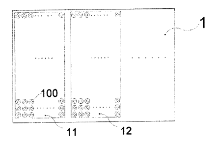
embodiment of the invention. As shown in FIG. 1, an electron source 1
comprises a plurality
of electron emission zones, such as electron emission zones 11, 12, etc.
Moreover, although
not shown, the electron source 1 may comprise only one electron emission zone.
As shown in
FIG. 1, each electron emission zone comprises a plurality of micro electron
emission units
100. Moreover, the micro electron emission units 100 in one identical electron
emission zone
are physically (electrically) connected with each other. Different electron
emission zones are
physically partitioned (i.e., different electron emission zones are
electrically isolated from
each other). Moreover, in FIG. 1, the plurality of electron emission zones 11,
12 ... are
arranged in a row along a width direction of the electron emission zones (left-
right direction
as shown in FIG. 1). However, the present invention is not limited thereto.
The electron
emission zones can also be arranged in other ways, for example arranged in
multiple rows, or
arranged in multiple rows with electron emission zones in every row staggered
with respect to
each other. Moreover, sizes and shapes of the electron emission zones and
intervals between
the electron emission zones can be arbitrarily set as needed.
[090] All the micro electron emission units 100 in one identical electron
emission zone
can simultaneously emit electrons or do not emit electrons at the same time.
The electron
emission zones can be controlled to emit electrons at a predetermined
sequence, such as, to
emit electrons successively, at intervals, alternatively, partially at the
same time, group by
group, or in other emission ways.
[091] FIG. 2 is a structural schematic diagram of a micro electron emission
unit 100
according to an embodiment of the invention. As shown in FIG. 2, the micro
electron
emission unit 100 comprises a base layer 101, an insulating layer 102 on the
base layer 101, a
grid layer 103 on the insulating layer 102, an opening 105 that penetrates
through the grid
layer 103 and the insulating layer 102 and reaches the base layer 101, and an
electron emitter
104 within the opening 105 fixed at the base layer 101. The base layer 101 is
a structural
foundation of the micro electron emission unit 100, which provides a
structural support and an
electric communication (electric connection). The insulating layer 102 is
arranged above the
13
CA 2919744 2017-06-08
base layer 101 and formed from insulating materials to insulate the grid layer
103 from the
base layer 101. Moreover, due to the supporting of the insulating layer 102,
the distances
between the grid layer and the base layer at various locations in one
identical electron
emission zone are on the whole kept equal (i.e., the surfaces at which the
grid layer and the
base layer respectively are located are parallel), such that an electric field
between the grid
layer 103 and base layer 101 is uniform. The grid layer 103 is arranged above
insulating layer
102 and formed from metal conductive material. The opening 105 penetrates
through the grid
layer 103 and the insulating layer 102. The electron emitter 104 is positioned
within the
opening 105 and connected to the base layer 101. Moreover, the opening 105 may
have any
processable shape, such as circular, square, polygon, oval and so on,
preferably circular. The
size (dimension) of the opening 105 within the grid layer 103 can be equal to
or different from
its size within the insulating layer 102. For example, as shown in FIG. 2, the
opening within
the insulating layer 102 is slightly larger than that within the grid layer
103. Moreover, the
electron emitter 104 is positioned within the opening 105 and connected to the
base layer 101.
Preferably, the electron emitter 104 is positioned at the center of the
opening. The linear
length direction of the electron emitter 104 is perpendicular to the surface
of the base layer
101. When an external power supply V applies a voltage difference between the
grid layer
103 and the base layer 101 (i.e., a field emission voltage), an electric field
is generated
between the grid layer 103 and the base layer 101. When the intensity of the
electric field
reaches a certain level, for example over 2V/m, the electron emitter 104
generates field
emission, wherein a generated electron beam current E penetrates the
insulating layer 102 and
the grid layer 103 and then exits from the opening 105.
[092] Moreover, the electron emitter 104 has a structure containing "nano-
materials".
The "nano-materials" describe, in a three dimensional space, materials of
which at least one
dimension is sized in a nanoscale (1-100 nm) or materials composed of basis
units at the
nanoscale. The "nano-materials" comprise metal or nonmetal nano-powder, nano-
fiber, nano-
film, nano-bulk and the like. Typical examples of the "nano-materials"
comprise carbon nano-
tube, zinc oxide nano-wire and so on. Preferably, the nano-materials in the
present invention
are single-walled carbon nano-tubes and double-walled carbon nano-tubes with a
diameter of
less than 10 nanometers.
14
CA 2919744 2017-06-08
[093] After studying and analyzing the Patent References 2-4, the inventor of
the
present invention realizes that, the electron emission units represented by
parts (A) and (B) of
FIG.3 generally have planar array arrangements, in which strip-shaped base
layers and grid
layers (or complex multi-level grid layers) are vertically and horizontally
(or longitudinally
and latitudinal) arranged. Each emission unit is independently controlled, and
has a very small
emission current. In applications, structural proportions of various
components are not
considered, and thus the quality of emission current is poor. In the structure
shown in the part
(B) of Fig. 3, the opening size of the grid layer is considerably larger than
the distance from
the nano-material to the grid layer, and thereby the edge of the nano-material
will experience
a strong electric field. The edge of the nano-material will first start
current emission. However,
the emitted current has large divergence angles at its edges, and thus has
poor forward
characteristics and will be easily blocked and absorbed by the grid layer. The
middle part of
the nano-material was supposed to generate emission current having good
forward
characteristics. However, since the electric field experienced by this part is
weak, there is no
or little emission current. The electron emission units represented by part
(C) of FIG. 3 are
definitely used in X-ray sources. There is a parallel planar structure between
the grid plane
and the nano-material plane, which has a large span and a small gap. Due to
restrictions in
terms of machining precision and installation accuracy, it is hard to make the
gap less than
2001am. Otherwise, two planes will not be parallel and thus the electric field
will not be
uniform; or a deformation of the grid itself or a deformation resulted from
the electric force
will substantially affect the uniformity of the electric field, even causing
short circuit between
the grid and the nano-material. Due to a large gap between the grid plane and
the nano-
material plane, such electron emission unit causes the control voltage for
field emission get
higher, which makes it more difficult to control and increase production cost.
As compared to
the existing structures shown in the parts (A), (B) and (C) of Fig. 3, the
present invention
provides a better electron emission characteristics and a larger electron beam
current E
through specific structures and ratios of various components of the micro
electron emission
unit 100 and the electron emission zones, while reducing the control voltage V
required for
field emission.
CA 2919744 2017-06-08
[094] Fig. 4 is a diagram that schematically shows a section view of a front
side of an
electron source 1 according to an embodiment of the invention. As shown in
Fig. 4, all micro
electron emission units 100 in an identical electron emission zone are
physically connected
(electrically connected). Specifically, for example, base layers 101 of
various micro electron
emission units 100 are the same substantive layer, grid layers 103 of various
micro electron
emission units 100 are the same substantive layer, and insulating layers 102
of various micro
electron emission units 100 are the same substantive layer. The term "same
substantive layer"
indicates the respective layers are located at the same spatial level,
electrically connected to
each other and structurally united together. The insulating layers 102 of
various micro
electron emission units 100 can also be composed of a plurality of insulating
pillars,
insulating blocks, insulating strips and so on that are located at the same
spatial level, so long
as the grid layer 103 and the base layer 101 can be insulated and have the
same distances
therebetween at various locations (i.e., the grid layer and the base layer are
parallel).
Moreover, the respective electron emission zones are physically partitioned.
Specifically, for
example, grid layers 103 of various electron emission zones are independent of
and separate
from each other, or base layers 101 of various electron emission zones are
independent of and
separate from each other, or both grid layers 103 and base layers 101 of
various electron
emission zones are independent of and separate from each other. Accordingly,
it is possible
that all micro electron emission units in an identical electron emission zone
can
simultaneously emit electrons or do not emit electrons at the same time, and
the respective
electron emission zones can be controlled to emit electrons at an
independently controlled
sequence or a combined controlled sequence. The simultaneous operations of a
plurality of
micro electron emission units 100 can cause an emission current of an electron
emission zone
larger than 0.8mA.
[095] Fig. 5 is a schematic diagram showing in its parts (A) ¨ (C) several
electron
sources segmented in different ways according to an embodiment of the
invention. As shown
in parts (A), (B) and (C) of Fig. 5, the physical partition between different
electron emission
zones can be achieved through various specific embodiments. For example, the
part (A) of
Fig. 5 shows that an electron emission zone 11 and an electron emission zone
12 have a
common base layer and a common insulating layer, but their grid layers are
separated with a
16
CA 2919744 2017-06-08
gap d; the part (B) of Fig. 5 shows that an electron emission zone 11 and an
electron emission
zone 12 have a common grid layer and a common insulating layer, but their base
layers are
separated with a gap d; and For example, the part (C) of Fig. 5 shows that all
of grid layers,
insulating layers and base layers of an electron emission zone 11 and an
electron emission
zone 12 are respectively separated with a gap d.
[096] Moreover, the shape of various electron emission zones can be square,
circular,
strip shape, oval, polygon, and other combined shapes and so on. The term
"rectangle"
indicates square or oblong, and the "oblong" means the ratio of its length and
width is larger
than 1 (for example, 10). Various electron emission zones of one electron
source may have
the same or different shapes. The various electron emission zones may have the
same or
different sizes. An electron emission zone can have a macro size of millimeter
level, such as
from 0.2mm to 40mm. The separation gap d between respective electron emission
zones may
be in a micrometer level, or may have a macro size of millimeter to centimeter
level. The
separation gaps d between different electron emission zones may be same or
different. In a
typical structure, each of electron emission zones has a strip shape with a
same size of lmm X
20mm, these electron emission zones are arranged in a parallel, regular and
even way along
their short edges (1mm), and the separation gap d between the various electron
emission
zones is lmm.
[097] Fig. 6 is a schematic diagram of a detail structure of a micro electron
emission unit
according to an embodiment of the invention. As shown in Fig. 6, in the
structure of the micro
electron emission unit 100, a base layer 101 provides both structural support
and electrical
connection, and can be a metal layer or can be composed of a substrate layer
106 and a
conducting layer 107. The substrate layer 106 is used to provide structural
support, such as
providing a smooth surface to which the conducting layer can be adhered. The
substrate layer
106 constitutes a structural foundation of the electron emission zone. That is
to say, the
adhesion, bonding, growth or fixation of the conducting layer 107, the
insulating layer 102,
the grid layer 103, the electron emitter 104 and so on are based on the
substrate layer 106. The
substrate layer 106 can comprise metal material, such as stainless steel, or
nonmetallic
material, such as ceramics. The conducting layer 107 is formed from materials
having good
17
CA 2919744 2017-06-08
conductivity, which can be metal or nonmetallic, such as gold, silver, copper,
molybdenum,
carbon nano film and so on.
[098] Moreover, a size S of a micro electron emission unit 100 in an electron
emission
zone along an array arrangement direction can be in a micrometer level. That
is to say, a
spatial dimension occupied by each micro electron emission unit 100 along the
array
arrangement direction is ranged from 1 m to 200pm, such as typically 50 um.
The direction
perpendicular to the array arrangement surface is defined as depth or
thickness. The thickness
of the substrate layer 106 may have a macro size of millimeter level, such as
lmm¨lOmm,
typically for example 4mm. Fig. 6 only shows a portion of the substrate layer
106 along its
thickness direction. The thickness of the conducting layer 107 may be at a
millimeter level or
a micrometer level, and has a certain relation to the material used. For easy
manufacture and
cost reduction, the thickness of the conducting layer 107 is preferably at a
micrometer level,
for example a carbon nano film with a thickness of 20 tun. The thickness of
the insulating
layer 102 may be at a micrometer level, such as from 5 Am to 400 um, typically
for example
100 um. The thickness of the grid layer 103 may be at a micrometer level, and
preferably is
close to but smaller than the thickness of the insulating layer 102, such as
from 5 m to
400 m, typically for example 30um. A dimension D of the opening 105 may be at
a
micrometer level, and may be smaller than the thickness of the insulating
layer 102, such as
m to 100um, typically for example 30 m. A height of the electron emitter 104
may be at a
micrometer level and smaller than half of the thickness of the insulating
layer 102, such as
1 um to 100 m, typically for example 20 m. A distance H from the electron
emitter 104 to
the grid layer 103 (i.e., the distance from the top of the electron emitter
104 to the lower edge
of the grid layer 103) may be at a micrometer level and smaller than the
thickness of the
insulating layer 102, i.e., smaller than 200 m, typically for example 80 m.
[099] The size S of the micro electron emission unit 100 may be at a
micrometer level
and the size D of the opening 105 may be at a micrometer level, such that a
number of single-
walled or double-walled carbon nano-tubes or a combination thereof with a
diameter of less
than 10 nanometers can be arranged within the opening 105, thereby ensuring a
certain
capability of current emission. The size of the opening 105 is less than the
thickness of the
18
CA 2919744 2017-06-08
insulating layer 102. That is to say, the opening 105 has a shape of "deep
well". The
distribution of electric field experienced by the top of the electron emitter
104 is relative
uniform, such that the emitted current from the electron emitter 104 has
relatively well
forward characteristic. The thickness of the grid layer 103 is close to but
smaller than the
thickness of the insulating layer 102, such that the electric field on the top
of the electron
emitter 104 is relative uniform and there is no significant block of an
electron beam current E
emitted by the electron emitter 104. The above structures and sizes of the
various components
improve the quality of the electron beam current E emitted by the micro
electron emission
unit 100, the intensity of the emission current and the forward
characteristics. Moreover, the
control voltage is adjusted such that the emission ability of each micro
electron emission unit
100 is larger than 100nA, such as from 100nA to 250..
[0100] Moreover, the distance H from the electron emitter 104 to the grid
layer 103 is
smaller than 20 m, such that the control voltage of the grid layer is smaller
than 500V (this is
because if a ration of a voltage between the grid layer and the electron
emitter to the distance
between the grid layer and the electron emitter is larger than 2V/Mm, the
electron emitter will
generate field emission. Actually, a nano-material tip of the electron emitter
has a great
intensity enhancement effect. That is to say, an electric field experienced by
the nano-material
tip will have a ratio larger than V/H, wherein V is the control voltage of the
grid layer, and H
is the distance between the grid layer and the electron emitter). Typically,
H=801..tm, the
control voltage V=300V. Accordingly, the electron source of the present
invention can be
easily controlled and have a low control cost.
[0101] Moreover, the size S of the micro electron emission unit 100 is at a
micrometer
level. According to above typical size ranges, the size S of the micro
electron emission unit
100 may be 50 m. An electron emission zone with an area of lmm X 20mm can
contain
8,000 micro electron emission units 100, each of which has an emission ability
of 100nA to
251.1A. The electron emission zone has a current emission ability over 0.8mA,
such as from
0.8mA to 200mA.
[0102] Moreover, the electron emitter 104 may be directly fixed on the
conducting layer
through growth, printing, bonding, sintering and so on, or may be fixed on
certain specifically
19
CA 2919744 2017-06-08
designed bulges on the conducting layer, for example as shown in parts (A),
(13) and (C) of
Fig. 7. The part (A) of Fig. 7 is a structural schematic diagram that shows a
nano-material is
fixed on a cone boss fixed. Alternatively, the boss may have a shape of
cuboid, cylinder and
so on, which are common structures in the art. The part (B) of Fig. 7 shows a
structure in
which a micro metal pillar (or metal tip) is arranged on the conducting layer
and nano-
materials are fixed on the metal pillar, thereby forming a tree shape of nano-
material. The part
(C) of Fig. 7 shows a structure in which the conducting layer is a film formed
of a nano-
material, and part of nano-material of the nano film within the opening stands
up by
subsequent process.
[0103] Fig. 8 is a structural schematic diagram of an X-ray source using an
electron
source according to an embodiment of the invention. The X-ray source shown in
Fig. 8
comprises: an electron source 1; an anode 2 arranged opposite to the electron
source 1; a
vacuum chamber 3 enclosing the electron source 1 and anode 2; an electron
source control
device 4 connected to the electron source 1; a high voltage power supply 5
connected to the
anode 2; a first connection unit 41 penetrating through a housing wall of the
vacuum chamber
3 and connected to the electron source 1 and the electron source control
device 4; and a
second connection unit 51 penetrating through a housing wall of the vacuum
chamber 3 and
connected to the anode 2 and the high voltage power supply 5.
[0104] As discussed above, the electron source 1 comprises at least one
electron emission
zone. The electron emission zone comprise a plurality of micro electron
emission units 100,
each of which occupies a spatial size at a micrometer level along the array
arrangement
direction. The micro electron emission unit 100 comprises a base layer 101, an
insulating
layer 102 on the base layer 101, a grid layer 103 on the insulating layer 102,
an opening 105
that penetrates through the grid layer 103 and the insulating layer 102 and
reaches the base
layer 101, and an electron emitter 104 within the opening 105 fixed at the
base layer 101. The
micro electron emission units 100 simultaneously emit electrons or do not emit
electrons at
the same time.
[0105] Furthermore, the operation state of the electron emission zone is
controlled by the
electron source control device connected to the electron source 1. The
electron source control
device applies two different voltages to the base layer 101 and the grid layer
103 in the
CA 2919744 2017-06-08
electron emission zone of the electron source 1 through a first connection
unit 41. An electric
field for field emission is established between the base layer 101 and the
grid layer 103, which
has a voltage difference V. The intensity of the electric field is V/H (H is a
distance between
the electron emitter 104 and the grid layer 103). When a voltage of the grid
layer 103 is higher
than a voltage of the base layer 101, V is positive. Otherwise, V is negative.
When the voltage
V of the electric field is positive, the nano-material of the electron emitter
104 is carbon
nanotube, and the intensity V/H is larger than 2V/[im (due to the intensity
enhancement effect
of the tip of the nano-material, the real electric field experienced by the
nano-material may be
larger than the value of V/H), the electron emission zone generates electron
emission. When
the voltage of the electric field is zero or negative, the electron emission
zone does not
generate electron emission. If both the voltage V and the intensity V/H
increase, the current
intensity of the electron emission will get higher. Therefore, the intensity
of the current
emitted from the electron source 1 may be adjusted through adjusting the
output voltage V of
the electron source control device 4. For example, an adjustable range of the
voltage that can
be outputted from the electron source control device 4 is from OV to 500V.
When the output
voltage is OV, the electron source 1 emits no electron. When the output
voltage reaches a
certain level, for example 200V, the electron source 1 starts emitting
electrons. When the
output voltage further increases to another level, for example 300V, the
current intensity of
electrons emitted from the electron source 1 achieves a target value. If the
current intensity
emitted from the electron source 1 is lower or higher than the target value,
turning up or down
the output voltage of the electron source control device 4 will cause the
current intensity
emitted from the electron source 1 back to the target value. This automatic
feedback
adjustment can be easily achieved in modem control systems. Normally, for
convenience of
use, the base layer 101 of the electron emission zone of the electron source 1
is connected to
ground potential, and a positive voltage is applied to the grid layer 103; or
the grid layer 103
is connected to ground potential, and a negative voltage is applied to the
base layer 101.
[0106] Moreover, the anode 2 is configured to establish a high voltage
electric field
between the anode 2 and the electron source 1 and receive an electron beam
current E which
is emitted from the electron source 1 and then accelerated by the high voltage
electric field,
thereby generating X-rays. The anode 2 is also known as target. Its material
usually is high-Z
21
CA 2919744 2017-06-08
metal materials, which is referred to as target materials. The widely used
materials comprise
tungsten, molybdenum, palladium, gold, copper, etc. Its material may be a
metal or alloy. For
cost reduction, a normal metal is usually used as a substrate, on which one or
more high-Z
materials as target materials are fixed through electroplating, sputtering,
high temperature
crimping, welding, bonding, etc.
[0107] The anode 2 is connected to an anode high voltage power supply 5
through a
second connection unit 51. The high voltage power supply 5 can generate a high
voltage of
dozens of kV to hundreds of kV (for example, 40 kV to 500 kV) which is applied
between the
anode 2 and the electron source 1. The anode 2 has a positive voltage with
respect to the
electron source 1. For example, in a typical example, main part of the
electron source 1 is
connected to ground potential, and a positive high voltage of 160 kV is
applied to the anode 2
through the high voltage power supply 5. A high voltage field is formed
between the anode 2
and the electron source 1. The electron beam current E emitted from the
electron source 1 is
accelerated by the high voltage field, moves along an electric field direction
(opposite to that
of line of electric force), and impinges on the target material of the anode
2, thereby
generating X-rays.
[0108] Moreover, the vacuum chamber 3 is an all-round hermetic hollow housing,
which
encloses the electron source 1 and the anode 2. The housing is mainly formed
of insulating
materials, such as glass, ceramics, etc. Alternatively, the housing of the
vacuum chamber 3
can be of metal material, such as stainless steel. When the housing of the
vacuum chamber 3
is made of metal materials, a sufficient distance is kept from the housing of
the vacuum
chamber 3 to the electron source 1 and anode 2 therein. This prevents
discharging and
electrical spark from occurring between the housing and the electron source 1
or the anode 2,
and does not affect an electric field distribution between the electron source
1 and the anode 2.
The first connection unit 41 is mounted at a wall of the vacuum chamber 3 to
pass electrical
cables through the wall of the vacuum chamber 3, while maintaining the sealing
of the
vacuum chamber 3. The first connection unit 41 is usually a lead terminal made
of ceramics.
The second connection unit 51 is mounted at a wall of the vacuum chamber 3 to
pass
electrical cables through the wall of the vacuum chamber 3, while maintaining
the sealing of
the vacuum chamber 3. The second connection unit 51 is usually a high voltage
lead terminal
22
CA 2919744 2017-06-08
made of ceramics. There is high vacuum within the vacuum chamber 3, which is
obtained
through drying and venting within a high temperature venting machine. The
vacuum level is
normally not lower than a level of 10-3 Pa, preferably not lower than a level
of 10-5 Pa. The
vacuum chamber 3 may comprise vacuum maintaining devices, such as ion pump and
so on.
[0109] Moreover, the electron source 1 comprises at least two electron
emission zones,
for example N electron emission zones. Each electron emission zone comprises a
plurality of
micro electron emission units 100. As described above, the micro electron
emission unit 100
comprises a base layer 101, an insulating layer 102 on the base layer 101, a
grid layer 103 on
the insulating layer 102, an opening 105 that penetrates through the grid
layer 103 and the
insulating layer 102 and reaches the base layer 101, and an electron emitter
104 within the
opening 105 fixed at the base layer 101. The micro electron emission units 100
in one
identical electron emission zone are physically connected, and different
electron emission
zones are physically partitioned.
[0110] As described above, the feature "the micro electron emission units 100
in one
identical electron emission zone are physically connected" means that their
base layers 101
are the same substantive layer, their grid layers 103 are the same substantive
layer, and their
insulating layers 102 are the same substantive layer. The feature "different
electron emission
zones are physically partitioned" may be the following circumstances. In
circumstance (A),
the base layers 101 and the insulating layers 102 of different electron
emission zones are
respectively the same layers, while the grid layers 103 of different electron
emission zones are
located on a same plane but partitioned. In this case, the base layers 101 of
the electron source
1 have a common lead which is connected to the electron source control device
4 through the
first connection unit 41. Each of the grid layers 103 of various electron
emission zones has a
separate lead which is connected to the electron source control device 4
through the first
connection unit 41. For a number of N electron emission zones, the first
connection unit 41
has at least N+1 separate leads. Moreover, the base layers 101 of the electron
source 1 are
connected to ground potential of the electron source control device 4 through
the common
lead, the multiple outputs (all of them having positive voltages) of the
electron source control
device 4 are connected to the respective grid layers 103 of various electron
emission zones
through the first connection unit 41, and thereby each electron emission zone
can be
23
CA 2919744 2017-06-08
independently controlled. In circumstance (B), the grid layers 103 and the
insulating layers
102 of different electron emission zones are respectively the same layers,
while the base
= layers 101 of different electron emission zones are located on a same
plane but partitioned.
For example, there is a gap d between neighboring electron emission zones.
When the base
layer 101 is composed of the non-conductive substrate layer 106 and the
conducting layer 107,
the partitions of the base layers 101 may be the case of partitions of the
conducting layer 107.
In this case, the grid layers 103 of the electron source 1 have a common lead
which is
connected to the electron source control device 4 through the first connection
unit 41. Each of
the base layers 101 of various electron emission zones has a separate lead
which is connected
to the electron source control device 4 through the first connection unit 41.
For a number of N
electron emission zones, the first connection unit 41 has at least N+1
separate leads. Moreover,
the grid layers 103 of the electron source 1 are connected to ground potential
of the electron
source control device 4 through the common lead, the multiple outputs (all of
them having
positive voltages) of the electron source control device 4 are connected to
the respective base
layers 101 of various electron emission zones through the first connection
unit 41, and thereby
each electron emission zone can be independently controlled. In circumstance
(C), different
electron emission zones are located on the same planes, while the grid layers
103, the
insulating layers 102 and the base layers 101 thereof are partitioned. For
example, there is a
gap d between neighboring electron emission zones. In this case, the base
layers 101 and the
grid layers 103 of the electron source 1 respectively have common leads which
are connected
to the electron source control device 4 through the first connection unit 41.
For a number of N
electron emission zones, the first connection unit 41 has at least 2N separate
leads. The
multiple outputs (wherein two of the leads compose a group, and there is a
voltage difference
between them) of the electron source control device 4 are respectively
connected to the base
layers 101 and the grid layers 103 of various electron emission zones through
the first
connection unit 41, and thereby each electron emission zone can be
independently controlled.
[0111] As shown in Fig. 8, a number of N electron emission zones 11, 12, 13
... at
different locations of the electron source 1 are arranged in a linear manner.
The electron
source 1 can emit electrons from the different locations. The anode 2 is
arranged opposite to
the electron source 1. That is, as shown in Fig. 8, the anode 2 is arranged
above the electron
24
CA 2919744 2017-06-08
source 1 and has a same or similar shape and size with those of the electron
source 1
respectively, and a surface on which target materials of the anode 2 are
provided is opposite to
the surface of the grid layers 103 of the electron source 1 in a parallel or
substantially parallel
manner. The electron beam current E generated from the electron emission zones
11, 12,
13 ... have a number of N X-ray target spots 21, 22, 23 ... at different
locations on the anode
2. In the present invention, the X-ray source which generates a plurality of X-
ray target spots
at different locations on an anode will be referred to as a distributed X-ray
source.
[0112] Fig. 9 is a schematic diagram of a distributed X-ray source according
to an
embodiment of the invention, in which an anode has a plurality of target
materials. As shown
in Fig. 9, the anode 2 of the distributed X-ray source comprises at least two
different target
materials, and thus can generate X-rays with different comprehensive energies
from different
target spot locations. X-ray is a continuous spectrum. The term "comprehensive
energy"
indicates a comprehensive effect reflected when proportions of X-rays with
various energies
vary. The electron source 1 comprises at least two electron emission zones.
The electron beam
current emitted from each electron emission zone generates X-ray target spots
at different
locations on the anode 2. Different target materials are provided at different
target spot
locations of the anode 2. Since different materials have different
characteristic spectrums, X-
rays with varying comprehensive energies can be obtained. For example,
molybdenum is
adopted as substrate of the anode 2, and on the surface of the anode 2 (which
is opposite to
the electron source 1), a tungsten target of a 200 pm thickness is deposited
at the X-ray target
spots 21, 23, 25 ... (which are opposite to the electron emission zones 11,
13, 15 ...) and a
copper target of a 200 m thickness is deposited at the X-ray target spots 22,
24, 26 ... (which
are opposite to the electron emission zones 12, 14, 16 ...) by ion sputtering.
When the X-ray
source operates at the same anode voltage, various electron emission zones
generate electron
beam currents E having same intensity and energy. However, a comprehensive
energy of an
X-ray X1 generated from the X-ray target spots 21, 23, 25 ... (tungsten
target) is larger than a
comprehensive energy of an X-ray X2 generated from the X-ray target spots 22,
24, 26 ...
(copper target).
[0113] Furthermore, Fig. 10 is a schematic diagram showing three operation
modes of a
distributed X-ray source according to an embodiment of the invention. As shown
in Fig.10,
CA 2919744 2017-06-08
the distributed X-ray source which uses the electron source 1 according to the
present
invention has multiple operation modes for achieving various beneficial
effects. A typical
= distributed X-ray source comprises an internal structure in which: the
electron emission zoncs
11, 12, 13 ... of the electron source 1 have the same strip shapes, and are
linearly arranged
along a narrow edge direction in the same plane in an even order. When the
number of the
electron emission zones is large (for example, dozens to thousands), the shape
of the electron
source 1 is also a strip shape, and the long edge direction of the electron
source 1 is
perpendicular to the long edge direction of the electron emission zone. The
associated anode 2
also has a strip shape, is aligned with the electron source 1 in an up-down
direction and is
parallel to the electron source 1. The distributed X-ray source can have
multiple operation
modes for providing various beneficial effects.
[0114] The first operation mode is mode A. A number of N electron emission
zones 11,
12, 13 ... independently emit electrons, and generate X-rays from the
corresponding N
positions on the anode 2 which form N target spots. In a first manner, the
electron emission
zones, according to their arranged locations, sequentially generate electron
beam emission for
a certain time T. That is to say, under the control of the electron source
control device 4, (1)
the electron emission zone 11 emits an electron beam, which generates X-ray
emission at the
position 21 on the anode 2, and stops the emission after a time period T; (2)
the electron
emission zone 12 emits an electron beam, which generates X-ray emission at the
position 22
on the anode 2, and stops the emission after a time period T; (3) the electron
emission zone 13
emits an electron beam, which generates X-ray emission at the position 23 on
the anode 2,
and stops the emission after a time period T; ... and so on. When all the
electron emission
zones have finished the first electron emission, another cycle starts with the
above step (1). In
a second manner, the electron emission zones that are partly partitioned
sequentially generate
electron beam emission for a certain time T. That is to say, under the control
of the electron
source control device 4, (1) the electron emission zone 11 emits an electron
beam, which
generates X-ray emission at the position 21 on the anode 2, and stops the
emission after a time
period T; (2) the electron emission zone 13 emits an electron beam, which
generates X-ray
emission at the position 23 on the anode 2, and stops the emission after a
time period T; (3)
the electron emission zone 15 emits an electron beam, which generates X-ray
emission at the
26
CA 2919744 2017-06-08
position 25 on the anode 2, and stops the emission after a time period T;...
and so on until the
terminal end of the electron source has been reached. Then, this part of the
electron emission
zones may emit once again, or other part of the electron emission zones (12,
14, 16 ...) may
emit concurrently. This process circulates. In a third manner, some of the
electron emission
zones are grouped together. The various groups sequentially generate electron
beam emission
for a certain time T. That is to say, under the control of the electron source
control device 4,
(1) the electron emission zones 11, 14 and 17 emits electron beams, which
generates X-ray
emission at the positions 21, 24 and 27 on the anode 2, and stops the emission
after a time
period T; (2) the electron emission zones 12, 15 and 18 emits electron beams,
which generates
X-ray emission at the positions 12, 15 and 18 on the anode 2, and stops the
emission after a
time period T; (3) the electron emission zones 13, 16 and 19 emits electron
beams, which
generates X-ray emission at the positions 23, 26 and 29 on the anode 2, and
stops the emission
after a time period T; ... and so on until all the groups finished electron
emission. This
process circulates. In the mode A, each electron emission zone is
independently controlled
and generates a separate target spot that corresponds to the electron emission
zone. Each
electron emission zone has a large width, for example a width of 2mm, and has
a large
emission current, for example larger than 1.6mA. Neighboring electron emission
zones have a
large gap, for example d=200, which corresponds to targets that have large
gaps (for example,
centre distance may be 2+2=4mm) and definite positions. Therefore, it can be
easily
controlled and used.
[0115] The second mode is mode B. From a number of N electron emission zones
11, 12,
13 ..., every n neighboring electron emission zones are grouped in a non-
overlapping manner.
The electron emission is executed by group. X-rays can be generated from the
corresponding
N/n positions on the anode 2, which form N/n target spots. For example, the
electron emission
zones (11, 12, 13) form group (1), the electron emission zones (14, 15, 16)
form group (2), the
electron emission zones (17, 18, 19) form group (3) ... and so on. The newly
formed N/3
(N/n=N/3) groups (1), (2), (3) ... can operate according to any of the
operation manners of
mode A. The mode B can provide several beneficial effects. On one side, the
combination of
the electron emission zones increases the intensity of the emission current,
and the intensity of
X-ray at each target spot is increased simultaneously. The number n may be set
according to
27
CA 2919744 2017-06-08
_ .
specific applications of the distributed X-ray source to obtain a desired
emission intensity of
electron beam. On the other side, the width of each electron emission zone may
be further
reduced, and more electron emission zones may be grouped together. When a
certain electron
emission zone malfunctions (for example, a certain micro electron emission
unit shorts) and
then is eliminated from the group, the group can still operate with the
emission current
reduced by 1/n. Such reduction can be compensated through parameter
adjustment. Therefore,
the distributed X-ray source as a whole still has N/n target spots, and there
is no "black spot"
(similar to black line on monitors) caused by malfunction of some electron
emission zone.
Avoidance of "black spot", on one side, can prevent blindness of X-ray target
spots and thus
reduce occurrence of malfunction. On the other side, if a few electron
emission zones
malfunction due to premature "failure", the means for avoiding "black spot"
actually extends
the life of the distributed X-ray source. Moreover, the group number n in this
mode can be a
fixed or unfixed value. For example, the number of electron emission zones in
a group may be
3, 5 and so on. The symbol "N/n" merely indicates that the group number and
the target spot
number is obtained through dividing the number N of the electron emission
zones by the
group factor n.
[0116] The third mode is mode C. From a number of N electron emission zones
11, 12,
13 ..., every n neighboring electron emission zones are grouped with "a"
(number a) of them
overlapped. The electron emission is executed by group. X-rays can be
generated from the
N - a N - a-
-
corresponding - " - a - positions on the anode, which form 1 nu _ target
spots. The
[N ¨ a N ¨ a
symbol ' indicates to round the result of n ¨ a to an integer. For example,
when n=3
and a=2, the electron emission zones (11, 12, 13) form group (1), the electron
emission zones
(14, 15, 16) form group (2), the electron emission zones (17, 18, 19) form
group (3) ... and so
on. Accordingly, there are formed N-2 groups (1), (2), (3)... which can
operate according to
any of the operation manners of mode A. The mode C can provide several
beneficial effects.
On one side, the mode C has the same advantages as the mode B, i.e.,
increasing of the
intensity of the emission electron beam current and avoidance of "black spot"
of the target
spots due to malfunction of some electron emission zones. On the other side,
as compared to
28
CA 2919744 2017-06-08
the mode B, the mode C has more target spots and smaller center distance
between the target
sports (neighboring target spots, corresponding to the groups of the electron
emission zones,
are partly overlapped). This is beneficial to the application of the
distributed X-ray source,
since both the number of the target spots and the number of the views are
increased, which
can substantially improve the image quality of the imaging system of the
distributed X-ray
source. As with the mode B, the factors n and "a" can be unfixed values. The
symbol
N ¨ al
G4 n¨a j"
merely indicates a calculation method, which means the number of the target
spots
in mode C is smaller than that in mode A but larger than that in mode B, which
provides an
advantage that its electron emission current is larger than that of the mode A
and the "black
spot" can be avoided.
[0117] The symbol N is a positive integer (N 3), the symbol n is a positive
integer
( N > n 2), and the symbol "a" is a positive integer ( n > a
[0118] Furthermore, the operation modes of the X-ray source of the present
invention are
not limited to the above three modes. Any mode is available, as long as the
electron emission
zones of the electron source 1 can emit electrons in a predetermined sequence
or a preset
number of neighboring electron emission zones of the electron source 1 can
emit electrons in
a predetermined sequence.
[0119] Furthermore, the above arrangement of the electron emission zones of
the electron
source 1 is only an exemplary specific structure. However, the arrangement of
the electron
emission zones may be arrangements of other shapes, irregular arrangements,
non-even
arrangements, multi-dimensional arrangements (for example, an array of 4 x
100), non-
coplanar arrangements, etc. All of them are embodiments of the electron source
1 of the
present invention. The associated anode 2 has a structure and shape that match
with the
arrangement of the electron emission zones. For example, patent documents such
as
CN203377194U, CN203563254U, CN203590580U and CN203537653U have disclosed
many arrangements. The electron emission zones of the present invention can
also be
arranged according to the manners disclosed in the above patent documents.
29
CA 2919744 2017-06-08
[0120] Fig. 11 is a schematic diagram showing a distributed X-ray source
according to an
embodiment of the invention, in which an electron source has a specific
structure. As shown
in Fig. 11, the electron emission zones of the electron source 1 have macro
widths, for
example from 2mm to 40mm, which is in a similar order of magnitude to the
distance from
the electron source 1 to the anode 2. For example, the ratio of the distance
between the
electron source 1 and the anode 2 to the width of the electron emission zone
is less than 10.
The surface of the electron emission zones has an arc shape in the width
direction (the left-
right direction in Fig. 11). Therefore, the electrons emitted from various
micro electron
emission units 100 in the electron emission zone have a better focusing
effect. The surface arc
of the electron emission zone may be provided to centre the target position on
the associated
anode 2. For example, the electron beam current E emitted from the electron
emission zone 11
generates the target spot 21 on the anode 2, and the surface of the electron
emission zone 11
(or the section thereof) is shown in the width direction as an arc the center
of which is located
at the target spot 21.
[0121] Fig. 12 is a schematic diagram of a distributed X-ray source having a
focusing
device according to an embodiment of the invention. As shown in Fig. 12, the
distributed X-
ray source further comprises a plurality of focusing devices 6 between the
electron source 1
and the anode 2, which are arranged to correspond to the electron emission
zones. The
focusing device 6 may be such as an electrode, a solenoid that can generate
magnetic field, or
the like. When the focusing device 6 is an electrode, it can be connected to
an external power
supply (or control system, not shown) through a focusing cable and connecting
means (not
shown) to obtain a pre-applied voltage (electric potential), such that the
electrons generated
from the micro electron emission units 100, when passing through the focusing
device 6, will
be focused toward the center. When the focusing device 6 is an electrode, it
may be an
electrode insulated from other components. When the various micro electron
emission units
100 emit electrons, a portion of electrons generated from the micro electron
emission units
100 at edges of the electron emission zone will be captured by the focusing
electrode to form
an electrostatic accumulation, thereby an electrostatic field will generate a
pushing force to
focus the subsequent electrons that pass through the focusing device 6 toward
the center.
When the focusing device 6 is a solenoid, it can be connected to an external
power supply (or
CA 2919744 2017-06-08
control system, not shown) through a focusing cable and connecting means (not
shown).
Accordingly, when a predetermined electric current flows through the solenoid
and then a
focusing magnetic field with a predefined intensity is generated above the
emission zone, the
electrons generated from the micro electron emission units 100, when passing
through the
focusing device 6, will be focused toward the center. In the present
invention, the focusing
devices are characterized in that they are arranged with respect to the
electron emission zones
in a one-to-one correspondence, and enclose all the micro electron emission
units 100 in the
electron emission zone from above. The focusing cable, connecting means,
external power
supply (or control system) not shown in Fig. 11 are customary means in the
art.
[0122] Fig. 13 is a schematic diagram showing in its parts (A) (D) several
collimation
effects of a distributed X-ray source according to an embodiment of the
invention. As shown
in Fig. 13, the distributed X-ray source further comprises a collimating
device 7, which is
disposed in an output path of X-ray for outputting X-rays in a shape of taper,
fan or pen, or
multiple parallel X-rays. The collimating device 7 may be an inner collimator
mounted within
the distributed X-ray source, or an outer collimator mounted outside of the
distributed X-ray
source. The materials of the collimating device 7 are generally high density
metal materials,
for example one or more of tungsten, molybdenum, depleted uranium, lead,
steel, etc. For
ease of description, a coordinate system is defined, in which a length
direction of the
distributed X-ray source (a target arrangement direction) is X direction, a
width direction of
the distributed X-ray source is Y direction, and an X-ray outputting direction
is Z direction.
As shown in the part (A) of Fig. 13, the collimating device 7 is provided in
the front of the
distributed X-ray source (along the X-ray outputting direction). In the
collimating device 7,
there are provided collimating slits with large widths. The arrangement length
of the
collimating slit approximates to the target distribution length of the
distributed X-ray source.
The collimating device 7 outputs taper X-ray beams each of which has a very
large angle in
the X direction and a large angle in the Y direction (the part (A) of Fig. 13
only shows a taper
X-ray beam generated from a center target spot). As shown in the part (B) of
Fig. 13, the
collimating device 7 is provided in the front of the distributed X-ray source.
There are very
narrow X-ray collimating slits in the collimating device 7. The arrangement
length of the
collimating slit approximates to the target distribution length of the
distributed X-ray source.
31
CA 2919744 2017-06-08
The collimating device 7 outputs X-ray beams each of which has a fan shape in
the X-Z plane
and a very small thickness in the Y direction (the part (B) of Fig. 13 only
shows a fan-shaped
X-ray beam generated from a center target spot). As shown in the part (C) of
Fig. 13, the
collimating device 7 is provided in the front of the distributed X-ray source.
The X-ray
collimating slits in the collimating device 7 are a series of slits that are
arranged in
corresponding to the target spot arrangement and each has a width (in the Y
direction). The
arrangement length of the collimating slit approximates to the target
distribution length of the
distributed X-ray source. The collimating device 7 outputs an array of X-ray
beams each of
which has a divergence angle in the Y direction and a thickness in the X
direction, wherein
the X-ray beams are seen as multiple parallel X-ray beams in the X-Z plane. As
shown in the
part (D) of Fig. 13, the collimating device 7 is provided in the front of the
distributed X-ray
source. The X-ray collimating slits in the collimating device 7 are a series
of small apertures
that are arranged in corresponding to the target spot arrangement. The
arrangement length of
the collimating slit approximates to the target distribution length of the
distributed X-ray
source. The collimating device 7 outputs an array of X-ray spot-beams in the X-
Y plane, each
of which is a pen-shaped X-ray beam that is coaxial with the Z-direction. All
the collimating
devices 7 shown in the parts (A), (B), (C) and (D) of Fig. 13 are provided
outside of the X-ray
source, and are used to modify the shapes of the X-ray beams in the outputting
path for X-ray.
However, the collimating device 7 can also be mounted within the X-ray source,
i.e., between
the anode 2 and the vacuum chamber 3. The collimating device 7 may be mounted
closer to
the anode 2 or the wall of the vacuum chamber 3. In this case, the collimating
device 7 is also
used to modify the shapes of the X-ray beams in the outputting path for X-ray.
When the
collimating device is mounted within the X-ray source, a reduction in size and
weight can be
achieved, and sometimes a better collimating effect is also obtained.
[0123] Fig. 14 is a schematic diagram of a distributed X-ray source in a
circular shape
according to an embodiment of the invention. As shown in Fig. 14, the target
spots of the
distributed X-ray source are arranged in a circle or a section of an arc. Fig.
14 shows a case
where the shape of the distributed X-ray source is a circle. Various electron
emission zones of
the electron source 1 are arranged in a circle, and the associated anodes 2
are also arranged in
a circle. The vacuum chamber 3 is provided as a circular ring that encloses
the electron source
32
CA 2919744 2017-06-08
1 and the anodes 2, the center of which is denoted as "0". The generated X-
rays point to the
center 0 or an axis in which the center 0 is positioned. The shapes of the
distributed X-ray
source can also be oval, three-quarter circle, semicircle, quarter circle, an
arc subtending other
angles, etc.
[0124] Fig. 15 is a schematic diagram of a distributed X-ray source in a box
shape
according to an embodiment of the invention. As shown in Fig. 15, the target
spots of the
distributed X-ray source are arranged in an enclosed rectangle, a polyline or
a section of a
straight line. Fig. 15 shows a case where the shape of the distributed X-ray
source is a
rectangular frame. Various electron emission zones of the electron source 1
are arranged in a
rectangular frame, and the associated anodes 2 are also arranged in a
rectangular frame. The
vacuum chamber 3 is provided as a rectangular frame that encloses the electron
source 1 and
the anodes 2. The generated X-rays point to the inside of the rectangular
frame. The shapes of
the distributed X-ray source can also be U-shape (three-quarter rectangle), L-
shape (half a
rectangle), straight line (quarter rectangle), equilateral polygon, other non-
right-angle
polylines, etc.
[0125] Fig. 16 is a schematic diagram showing in its parts (A) ¨ (D) several
section views
of a distributed X-ray source according to an embodiment of the invention. As
shown in Fig.
16, the targets on the anode 2 of the distributed X-ray source may be
transmission target or
reflection target.
[0126] The part (A) of Fig. 16 shows a case where the anode targets of the
distributed X-
ray source are transmission targets. That is to say, in this case, the
outputting direction of the
X-ray is substantially same with the incoming direction of the electron beam
current E. In
connection with Fig. 14, the part (A) of Fig. 16 may be interpreted that:
various electron
emission zones of the electron source 1 are arranged in an outer circle, and
the surfaces of the
electron emission zones are parallel to the axis of the circle; various target
spots of the anodes
2 are arranged in an inner circle, which is concentric with the outer circle;
the vacuum
chamber 3 is a hollow circular ring that encloses the electron source 1 and
the anode 2; there
is provided a thin thickness at the target locations of the anode 2, for
example less than lmm;
and the directions of the electron beam current E and the X-ray both point to
the center 0 of
the circle. In connection with Fig. 15, the part (A) of Fig. 16 may be
interpreted that: various
33
CA 2919744 2017-06-08
=
electron emission zones are arranged in an outer rectangle, and the surfaces
of the electron
emission zones are parallel to a center axis of the rectangle; various target
spots of the anodes
2 are arranged in an inner rectangle, the center of which coincides with that
of the outer
rectangle; the vacuum chamber 3 is a hollow rectangular ring that encloses the
electron source
1 and the anode 2; there is provided a thin thickness at the target locations
of the anode 2, for
example less than lmm; and the directions of the electron beam current E and
the X-ray both
point to the inside of the rectangles.
[0127] The part (B) of Fig. 16 shows a case where the anode targets of the
distributed X-
ray source are reflection targets. That is to say, in this case, an angle of
90 degrees is formed
between the outputting direction of the X-ray and the incoming direction of
the electron beam
current E (the angle of 90 degrees herein includes an angle of about 90
degree, wherein the
angle range may be from 70 to 120 degree, preferably from 80 to 100 degree).
In connection
with Fig. 14, the part (B) of Fig. 16 may be interpreted that: various
electron emission zones
of the electron source 1 are arranged in a circle, and the surfaces of the
electron emission
zones are perpendicular to an axis 0 of the circle; various target spots of
the anodes 2 are
arranged in another circle, wherein the two circles have the same size and
their centers are
located at the circle axis, and planes at which the above two circles are
provided are parallel
to each other; or furthermore, the anode 2 has an inclined angle (for example,
10 degree) with
respect to the electron source 1 such that a surface in which the various
target spots of the
anode 2 are arranged is a conical surface, an axis of which coincides with the
circle axis. The
vacuum chamber 3 is a hollow circular ring that encloses the electron source 1
and the anode
2. The direction of the electron beam current E is parallel to the circle
axis, and the direction
of the X-ray points to the center 0 of the circle. In connection with Fig. 15,
the part (B) of Fig.
16 may be interpreted that: various electron emission zones are arranged in a
rectangle, and
the surfaces of the electron emission zones are parallel to a center axis 0 of
the rectangle;
various target spots of the anodes 2 are arranged in another rectangle,
wherein the two
rectangles have the same size and planes at which the two rectangles are
provided are parallel
to each other; or furthermore, the anode 2 has an inclined angle (for example,
10 degree) with
respect to the electron source 1 such that a surface in which the various
target spots of the
anode 2 are arranged is a pyramid surface, a center line of which coincides
with that of the
34
CA 2919744 2017-06-08
S
rectangles. The vacuum chamber 3 is a hollow rectangular ring that encloses
the electron
source 1 and the anode 2. The direction of the electron beam current E is
parallel to the center
line of the rectangle, and the direction of the X-ray points to the inside of
the rectangle.
[0128] Furthermore, a light source shown in the part (C) of Fig. 16 is also a
transmission
target. As compared to the part (A) of Fig. 16, the difference is only in the
arrangements of
the electron source 1 and the anode 2 in the circle (or rectangle), i.e.,
replacing outer-inner
circles (or outer-inner rectangles) by front-back circles (or front-back
rectangles). The
directions of the electron beam current E and the X-ray both are parallel to
the axis of circle
(or the center line of rectangle). That is to say, the distributed X-rays are
emitted in a
transverse direction of the circle (or a transverse direction of the
rectangle).
[0129] Furthermore, a light source shown in the part (D) of Fig. 16 is also a
reflection
target. As compared to the part (B) of Fig. 16, the difference is only in the
arrangements of the
electron source 1 and the anode 2 in the circle (or rectangle), i.e.,
replacing outer-inner circles
(or outer-inner rectangles) by front-back circles (or front-back rectangles).
The direction of
the electron beam current E is perpendicular to the center line of the circle
(or the center line
of the rectangle), and the direction of the X-ray is parallel to the axis of
circle (or the center
line of rectangle). That is to say, the distributed X-rays are emitted in a
transverse direction of
the circle (or a transverse direction of the rectangle).
[0130] Strictly speaking, only the part (A) of Fig. 16 corresponds to Fig. 14
and Fig.15,
while the part (B) of Fig. 16 corresponds to Fig. 14. By making reference to
the description of
Fig. 15, it is convenient to explain the part (B) of Fig. 16.
[0131] Moreover, the shape of the distributed X-ray source may be a
combination of the
above described curves and strait lines, or spiral and the like, any of which
is processable for
modern processing technology.
[0132] Fig. 17 is a schematic diagram of an X-ray transmission imaging system
using a
distributed X-ray source according to an embodiment of the invention. Fig. 17
shows the
transmission imaging system using the distributed X-ray source of the present
invention
comprises at least one X-ray source 81 according to the present invention, for
generating X-
rays able to cover a detection area; at least one detector 82 disposed at
other side of the
detection area and opposite to the X-ray source 81, for receiving the X-rays;
and a
CA 2919744 2017-06-08
transporting device 84 disposed between the X-ray source 81 and the detector
82, for carrying
a detected object 83 through the detection area.
[0133] A first specific embodiment comprises: one X-ray source, which has one
electron
emission zone and forms one X-ray target spot; and a plurality of detectors,
which form a
linear array or a planar array (or a planar detector). This embodiment has a
configuration
similar to existing X-ray transmission imaging system. This embodiment
provides a simple
structure, a small size and a low cost. However, the field emission X-ray
source of the present
invention has advantages of lower control voltage and fast start-up speed.
[0134] A second specific embodiment comprises: one X-ray source, which has two
electron emission zones, wherein two X-ray target spots have different target
materials and
can alternately generate two X-ray beams with different energies; and a
plurality of detectors,
which form a linear array or a planar array (or a planar detector), or serving
as dual energy
detectors. This embodiment provides a simple structure, a small size and a low
cost, and can
achieve dual energy imaging, which improves ability to identify materials of
detected objects.
[0135] A third specific embodiment comprises: one distributed X-ray source,
which has a
plurality of X-ray target spots; and a plurality of detectors, which form a
linear array or a
planar array (or a planar detector). These detectors perform transmission
imaging to the
detected object at different angles (locations), thereby obtaining a
transmission image
comprising multilevel information in a depth direction. Compared to a multi-
view system
using a number of normal X-ray source, this embodiment provides a simple
structure, a small
size and a low cost.
[0136] A fourth specific embodiment comprises: one distributed X-ray source,
which has
a plurality of X-ray target spots; and one or several detectors, which obtains
transmission
images through a "reverse" imaging principle. This embodiment is characterized
in reduction
of detector number and cost.
[0137] A fifth specific embodiment comprises: one or more distributed X-ray
sources and
one or more associated detector arrays, wherein all X-ray target spots are
arranged to surround
the detected object and the surrounding angle is larger than 180 degree. This
embodiment
provides a large surrounding angle arrangement of static X-ray source to
obtain a complete
36
CA 2919744 2017-06-08
3D transmission image of the detected object, thereby enabling a fast
detection speed and a
high efficiency.
[0138] A sixth specific embodiment comprises: a plurality of distributed X-ray
sources
and a plurality of associated detector arrays, which are arranged in a
plurality of planes along
a delivery direction of the detected object. This embodiment is characterized
in improving the
detection speed multiply, or forming multi-energy 3D transmission images in
different planes
with X-rays of different energies, or progressively improving quality of
detection images. For
example, a first plane roughly detects suspicious areas, a second plane
performs a careful
detection to the suspicious areas through different parameters, thereby high
resolution and
sharpness images can be obtained.
[0139] Fig. 18 is a schematic diagram of a back scattering imaging system
using a
distributed X-ray source according to an embodiment of the invention. Fig. 18
shows the back
scattering imaging system using the distributed X-ray source of the present
invention
comprises: at least one distributed X-ray source 81 according to the present
invention, for
generating a number of pen-shaped X-ray beams to cover a detection area; and
at least one
detector 82 disposed at the same side of the detection area and opposite to
the X-ray source 81,
for receiving the X-rays that are reflected from a detected object.
[0140] A first specific embodiment further comprises: a transporting device 84
for
carrying the detected object 83 through the detection area to accomplish an
overall imaging of
the detected object.
[0141] A second specific embodiment further comprises: a movement device for
moving
the distributed X-ray source 81 and the detected object 82 such that the
detection area can
scan the detected object to accomplish an overall imaging of the detected
object.
[0142] A third specific embodiment comprises: at least two groups of the
distributed X-
ray sources 81 and the detectors 82, disposed at different sides of the
detected object. By
moving the detected object through the transporting device or moving the X-ray
source
through a movement device, an "all round" imaging of the detected object is
accomplished.
[0143] Moreover, an X-ray detection system is provided, which comprises: at
least two
distributed X-ray sources of the present invention; at least two groups of
detectors that
correspond to the X-ray sources; and an image comprehensive process system. At
least one
37
CA 2919744 2017-06-08
=
group of the distributed X-ray source and the detector is used to perform a
transmission
imaging to a detected object. At least one group of the distributed X-ray
source and the
detector is used to perform a back scattering imaging to the detected object.
The image
comprehensive process system is used to comprehensively process the
transmission images
and the back scattering images, thereby obtaining more characteristic
information of the
detected object.
[0144] Furthermore, it should be particularly noted that, the above X-ray
transmission
imaging system and back scattering imaging system may be common arrangement on
ground,
or may be integrated into movable devices, for example vehicles, to constitute
a movable
transmission imaging system and a movable back scattering imaging system.
[0145] Furthermore, it should be particularly noted that, the above
transmission imaging
system and back scattering imaging system have general meanings. By adding
auxiliary
components or not, the above systems can be used to detect such as small
vehicles, freights,
luggage, baggage, mechanical components, industry products, personnel, body
parts and so on.
[0146] Furthermore, a real-time image-guided radiotherapy equipment is
provided, which
comprises: a radiotherapy radiation source, for generating radiation beams for
radiotherapy of
a patient; a multi-leaf collimator for adjusting shapes of the radiation beams
for radiotherapy
to adapt to a lesion; a movable bed for moving and locating the patient such
that the position
of the radiation beam for radiotherapy aligns with the position of the lesion;
at least one
distributed X-ray source of the present invention for generating radiation
beams for
performing a diagnostic imaging to the patient; a planar detector for
receiving the radiation
beams for diagnostic imaging; a control system, for forming a diagnostic image
according to
the radiation beams received by the planar detector, locating the position of
the lesion in the
diagnostic image, aligning centers of the radiation beams for radiotherapy
with the center of
the lesion, and matching the shapes of the radiation beams for radiotherapy of
the multi-leaf
collimator with the shape of the lesion. The distributed X-ray source is a
distributed X-ray
source that has a circle or rectangle shape and outputs X-rays in a transverse
direction (the
cases shown in the parts (C) and (D) of Fig. 16). The axis or center line of
the distributed X-
ray source is in line with the beam axis of the radiotherapy radiation source.
That is to say, the
radiotherapy radiation source and the diagnostic radiation source are located
at the same side
38
CA 2919744 2017-06-08
of the patient. The planar detector is located at the other side of the
patient with respect to the
diagnostic radiation source. It is possible to perform an image-guided
radiotherapy to the
patient and obtain the diagnostic image at the same time, without rotating
cantilevers of the
radiotherapy equipment. This is a "real-time" image-guided radiotherapy.
Regarding therapy
of body parts having physiological movements, for example lung, heart and so
on, the "real-
time" image-guided radiotherapy can decrease exposure doses and reduce
exposure to normal
organics, which is very important. Moreover, the distributed X-ray source of
the present
invention has a number of target spots and thus can obtain "three-dimensional"
diagnostic
images having depth information, which differ from normal planar images. In
the image-
guided radiotherapy, this can further improve the guiding accuracy and
locating precision of
the radiation beams for radiotherapy.
[0147] As described above, the present invention is illustrated, but not
limited to this. It
should be understood that various combinations and alterations within the
spirit of the present
invention, and any device, equipment or system that adopts the electron source
of the present
invention or the X-ray source of the present invention are within the scope of
the present
invention.
[0148] Reference Sign List:
1: Electron Source;
11, 12, 13: Electron Emission Zones at Electron Source;
100: Micro Electron Emission Unit;
101: Base Layer;
102: Insulating Layer;
103: Grid Layer;
104: Electron Emitter;
105: Opening;
106: Substrate Layer;
107: Conducting Layer;
2: Anode;
21, 22, 23: X-ray Target Spots at Anode;
39
CA 2919744 2017-06-08
- =
3: Vacuum Chamber;
4: Electron Source Control Device;
41: First Connection Unit;
5: High Voltage Power Supply;
51: Second Connection Unit;
6: Focusing Device;
7: Collimating Device;
81: X-ray Source;
82: Detector;
83: Detected Object;
84: Transporting device;
S: Size of Micro Electron Emission Unit;
D: Size of Opening;
II: Distance from Electron Emitter to Grid Layer;
h: Height of Electron Emitter;
d: Interval between Electron Emission Zones;
V: Field Emission Voltage;
E: Electron Beam Current:
X: X-ray;
0: Center, Centerline or Axis of X-ray Source
CA 2919744 2017-06-08