Note: Descriptions are shown in the official language in which they were submitted.
CA 02919985 2016-01-29
WO 2015/017730 PCT/US2014/049297
APERTURE SCANNING FOURIER PTYCHOGRAPHIC IMAGING
CROSS-REFERENCES TO RELATED APPLICATIONS
[0001] This application claims benefit of U.S. Provisional Patent Application
No.
61/860,786, titled "Generalized Ptychographic Imaging with Optical Transfer
Function Modulation" and filed on July 31, 2013 and U.S. Provisional Patent
Application No. 61/868,967, titled "Alternative Optical Implementations for
Fourier
Ptychographic Microscopy" and filed on August 22, 2013, both of which are
hereby
incorporated by reference in their entirety and for all purposes.
BACKGROUND OF THE INVENTION
[0002] Certain embodiments described herein generally relate to imaging
techniques, and more specifically to methods, devices, and systems for Fourier
ptychographic imaging. Certain embodiments may be used in applications such
as, for
example, microscopy and/or photography.
[0003] Imaging lenses ranging from microscope objectives to satellite-based
cameras are physically limited in the total number of features they can
resolve. These
limitations are a function of the point-spread function (PSF) size of the
imaging
system and the inherent aberrations across its image plane field of view
(FOV).
Referred to as the space-bandwidth product, the physical limitation scales
with the
dimensions of the lens but is usually on the order of 10 megapixels regardless
of the
magnification factor or numerical aperture (NA). A discussion of space-
bandwidth
product of conventional imaging systems can be found in Lohmann, A. W.,
Dorsch,
R. G., Mendlovic, D., Zalevsky, Z. & Ferreira, C., "Space¨bandwidth product of
optical signals and systems," J. Opt. Soc. Am. A. 13, pages 470-473 (1996),
which is
hereby incorporated by reference for this discussion. While conventional
imaging
systems may be able to resolve up to 10 megapixels, there is typically a
tradeoff
between PSF and FOV. For example, certain conventional microscope objectives
can
offer a sharp PSF (e.g., 0.5 [Lm) across a narrow FOV (e.g., lmm), while
others
imaging systems with wide-angle lenses can offer a wide FOV (e.g., lOmm) at
the
expense of a blurry PSF (e.g., 5 [Lm).
1
CA 02919985 2016-01-29
WO 2015/017730 PCT/US2014/049297
[0004] Certain interferometric synthetic aperture techniques that try to
increase
spatial-bandwidth product are described in Di, J. et at., "High resolution
digital
holographic microscopy with a wide field of view based on a synthetic aperture
technique and use of linear CCD scanning," Appl. Opt. 47, pp. 5654-5659
(2008);
Hillman, T. R., Gutzler, T., Alexandrov, S. A., and Sampson, D. D., "High-
resolution,
wide-field object reconstruction with synthetic aperture Fourier holographic
optical
microscopy," Opt. Express 17, pp. 7873-7892 (2009); Granero, L., Mid), V.,
Zalevsky, Z., and Garcia, J., "Synthetic aperture superresolved microscopy in
digital
lensless Fourier holography by time and angular multiplexing of the object
information," Appl. Opt. 49, pp. 845-857 (2010); Kim, M. et at., "High-speed
synthetic aperture microscopy for live cell imaging," Opt. Lett. 36, pp. 148-
150
(2011); Turpin, T., Gesell, L., Lapides, J., and Price, C., "Theory of the
synthetic
aperture microscope," pp. 230-240; Schwarz, C. J., Kuznetsova, Y., and Brueck,
S.,
"Imaging interferometric microscopy," Optics letters 28, pp. 1424-1426 (2003);
Feng,
P., Wen, X., and Lu, R., "Long-working-distance synthetic aperture Fresnel off-
axis
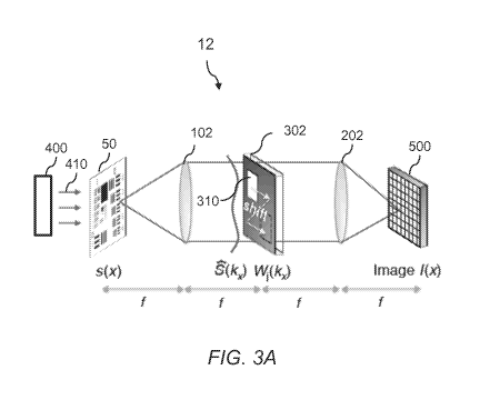
digital holography," Optics Express 17, pp. 5473-5480 (2009); Mico, V.,
Zalevsky,
Z., Garcia-Martinez, P., and Garcia, J., "Synthetic aperture superresolution
with
multiple off-axis holograms," JOSA A 23, pp.3162-3170 (2006); Yuan, C., Zhai,
H.,
and Liu, H., "Angular multiplexing in pulsed digital holography for aperture
synthesis," Optics Letters 33, pp. 2356-2358 (2008); Mico, V., Zalevsky, Z.,
and
Garcia, J., "Synthetic aperture microscopy using off-axis illumination and
polarization
coding," Optics Communications, pp. 276, 209-217 (2007); Alexandrov, S., and
Sampson, D., "Spatial information transmission beyond a system's diffraction
limit
using optical spectral encoding of the spatial frequency," Journal of Optics
A: Pure
and Applied Optics 10, 025304 (2008); Tippie, A.E., Kumar, A., and Fienup,
J.R.,
"High-resolution synthetic-aperture digital holography with digital phase and
pupil
correction," Opt. Express 19, pp. 12027-12038 (2011); Gutzler, T., Hillman,
T.R.,
Alexandrov, S.A., and Sampson, D.D., "Coherent aperture-synthesis, wide-field,
high-resolution holographic microscopy of biological tissue," Opt. Lett. 35,
pp. 1136-
1138 (2010); and Alexandrov, S.A., Hillman, T.R., Gutzler, T., and Sampson,
D.D.,
"Synthetic aperture Fourier holographic optical microscopy," Phil. Trans. R.
Soc.
Lond. A 339, pp. 521-553 (1992), all of which are hereby incorporated by
reference
for the discussion of attempts to increase spatial bandwidth. Most of the
above-
2
CA 02919985 2016-01-29
WO 2015/017730 PCT/US2014/049297
described interferometric synthetic aperture techniques include setups that
record both
intensity and phase information using interferometric holography such as off-
line
holography and phase-shifting holography. Interferometric holography has its
limitations. For example, interferometric holography recordings typically use
highly
coherent light sources. As such, the constructed images typically suffer from
coherent
noise sources such as speckle noise, fixed pattern noise (induced by
diffraction from
dust particles and other optical imperfections in the beam path), and multiple
interferences between different optical interfaces. Thus the image quality is
typically
worse than from a conventional microscope. On the other hand, using off-axis
holography sacrifices spatial-bandwidth product (i.e., reduces total pixel
number) of
the image sensor. A discussion of certain off-axis holography methods can be
found
in Schnars,U. and Jiiptner,W.P.O., "Digital recording and numerical
reconstruction of
holograms," Measurement Science and Technology, 13, R85 (2002), which is
hereby
incorporated by reference for this discussion. In addition, interferometric
imaging
techniques may subject to uncontrollable phase fluctuations between different
measurements. Hence, accurate a priori knowledge of the sample location may be
needed to set a reference point in the image recovery process. Another
limitation is
that many of these interferometric imaging systems require mechanical scanning
to
rotate the sample and thus precise optical alignments, mechanical control at a
sub-
micron level, and associated maintenances are required by these systems. In
terms of
spatial-bandwidth product, these interferometric imaging systems may present
little to
no advantage as compared with a conventional microscope.
[0005] Previous lensless microscopy such as digital in-line holography and
contact-
imaging microscopy also present drawbacks. For example, conventional digital
in-
line holography does not work well with contiguous samples and contact-imaging
microscopy requires a sample to be in close proximity to the sensor. A
discussion of
certain digital in-line holography devices can be found in Denis, L., Lorenz,
D.,
Thiebaut, E., Fournier, C. and Trede, D., "Inline hologram reconstruction with
sparsity constraints," Opt. Lett. 34, pp. 3475-3477 (2009); Xu, W., Jericho,
M.,
Meinertzhagen, I., and Kreuzer, H., "Digital in-line holography for biological
applications," Proc. Natl Acad. Sci. USA 98, pp. 11301-11305 (2001); and
Greenbaum, A. et al., "Increased space¨bandwidth product in pixel super-
resolved
3
CA 02919985 2016-01-29
WO 2015/017730 PCT/US2014/049297
lensfree on-chip microscopy," Sci. Rep. 3, page 1717 (2013), which are hereby
incorporated by reference for this discussion. A discussion of certain contact-
imaging
microscopy can be found in Zheng, G., Lee, S. A., Antebi, Y., Elowitz, M. B.
and
Yang, C., "The ePetri dish, an on-chip cell imaging platform based on subpixel
perspective sweeping microscopy (SPSM)," Proc. Natl Acad. Sci. USA 108, pp.
16889-16894 (2011); and Zheng, G., Lee, S. A., Yang, S. & Yang, C., "Sub-pixel
resolving optofluidic microscope for on-chip cell imaging," Lab Chip 10, pages
3125-3129 (2010), which are hereby incorporated by reference for this
discussion.
[0006] A high spatial-bandwidth product is very desirable in microscopy for
biomedical applications such as digital pathology, haematology, phytotomy,
immunohistochemistry, and neuroanatomy. For example, there is a strong need in
biomedicine and neuroscience to digitally image large numbers of histology
slides for
evaluation. This need has prompted the development of sophisticated mechanical
scanning and lensless microscopy systems. These systems increase spatial-
bandwidth product using complex mechanisms with high precision to control
actuation, optical alignment, and motion tracking. These complex mechanisms
tend
to be expensive to fabricate and difficult to use and maintain.
BRIEF SUMMARY OF THE INVENTION
[0007] Aspects of this disclosure concern imaging techniques, and more
specifically
methods, devices, and systems for Fourier ptychographic imaging, which may be
used
in applications such as, for example, microscopy and photography.
[0008] Certain aspects pertain to aperture-scanning Fourier ptychographic
imaging
devices comprising optical elements, an aperture scanner that can generate an
aperture
at a plurality of locations at an intermediate plane of the optical elements,
and a
detector that can acquire lower resolution intensity images for different
aperture
locations, and wherein a higher resolution complex image may be constructed by
iteratively updating regions in Fourier space with the acquired lower
resolution
images.
[0009] In some aspects, an aperture-scanning Fourier ptychographic imaging
device
comprises a first optical element configured to receive light from a sample
and a
second optical element. The device further comprises an aperture scanner
configured
4
CA 02919985 2016-01-29
WO 2015/017730 PCT/US2014/049297
to generate an aperture at a plurality of aperture locations in an
intermediate plane, the
aperture configured to pass incident light at the aperture from the first
optical element
to the second optical element. The device further comprises a radiation
detector
configured to receive light from the second optical element and to acquire a
plurality
of intensity images associated with different aperture locations. The device
further
comprises a processor configured to construct a complex image of the sample by
iteratively updating regions in Fourier space with the acquired intensity
images.
[0010] In some aspects, a aperture-scanning Fourier ptychographic imaging
method
comprises illuminating a sample, receiving incident light at a first optical
element
from the sample, generating an aperture at a plurality of locations at an
intermediate
plane, passing incident light at the aperture from the first optical element
to a second
optical element. The method further comprises acquiring a plurality of
intensity
images using a detector receiving light from the second optical element and
constructing a complex image of the sample by iteratively updating regions in
Fourier
space with the plurality of intensity images.
[0011] These and other features are described in more detail below with
reference
to the associated drawings.
BRIEF DESCRIPTION OF THE DRAWINGS
[0012] Figure 1 illustrates a schematic drawing of components of a Fourier
ptychographic imaging system with optical transfer function modulation at the
intermediate plane.
[0013] Figures 2A and 2B are schematic drawings of components of an aperture-
scanning Fourier ptychographic imaging system.
[0014] Figure 3A is a schematic drawing of components of an aperture-scanning
Fourier ptychographic imaging system.
[0015] Figure 3B is a schematic drawing of cross-sectional view of a display
of a
spatial light modulator that can be implemented in certain aperture-scanning
Fourier
ptychographic imaging systems.
5
CA 02919985 2016-01-29
WO 2015/017730 PCT/US2014/049297
[0016] Figure 4 is a schematic drawing of components of an aperture-scanning
Fourier ptychographic imaging system comprising a DMD array.
[0017] Figure 5 is a schematic drawing of components of an aperture-scanning
Fourier ptychographic imaging system comprising a DMD array.
[0018] Figure 6 is a schematic drawing of a view of components of an aperture-
scanning Fourier ptychographic imaging system comprising an LCOS array.
[0019] Figure 7 is a schematic diagram of components of an aperture-scanning
Fourier ptychography imaging system.
[0020] Figure 8 is a flowchart of an aperture-scanning Fourier ptychography
imaging method performed by an aperture-scanning Fourier ptychography imaging
system.
[0021] Figure 9 is an aperture-scanning Fourier ptychography imaging method
with
digital wavefront correction.
[0022] Figure 9A is a flowchart of an example of sub-steps of one or more
steps of
the method of Figure 8.
[0023] Figure 9B is a flowchart of another example of sub-steps of one or more
steps of the method of Figure 8.
[0024] Figure 10 is a flowchart of an aperture scanning Fourier ptychographic
method with tile imaging, according to certain aspects.
[0025] Figure 11 is a block diagram of subsystems that may be present in
aperture-
scanning Fourier ptychography imaging system.
DETAILED DESCRIPTION OF THE INVENTION
[0026] Embodiments of the present invention will be described below with
reference to the accompanying drawings. The features illustrated in the
drawings may
not be to scale.
[0027] I. Introduction
[0028] Fourier ptychography imaging implements a phase retrieval technique
that
uses angular diversity to recover complex sample images. The recovery process
6
CA 02919985 2016-01-29
WO 2015/017730 PCT/US2014/049297
comprises alternating enforcement of known sample information in the spatial
domain
and a fixed constraint in the Fourier domain. The phase retrieval recovery may
be
implemented using any variant of an alternating projections algorithm, a
convex
reformulation of the problem, or any non-convex variant in-between. Instead of
shifting a sample laterally (i.e. applying translational diversity), Fourier
ptychography
imaging uses a scanning spectrum constraint in the Fourier domain to expand
the
Fourier passband beyond that of a single captured image to recover an improved-
resolution complex sample image.
[0029] Certain variable-angle illumination Fourier ptychography imaging
systems
use a variable illumination source (e.g., an LED array) to illuminate a sample
being
imaged from different illumination angles successively. An optical element
such as a
low numerical aperture objective lens filters light from the sample. A
radiation
detector receives the filtered light from the optical element and captures a
intensity
image of the sample at each illumination angle. Multiple resolution images may
be
iteratively stitched together in the Fourier domain to recover a higher
resolution image
of the image. Details of some variable-angle illumination Fourier ptychography
systems, devices, and methods can be found in U.S. Patent Application Serial
Number
14/065,280, titled "Fourier Ptychographic Imaging Systems, Devices, and
Methods"
and filed on October 28, 2013 and in U.S. Patent Application Serial Number
14/065,305, titled "Fourier Ptychographic X-ray Imaging Systems, Devices, and
Methods," which are hereby incorporated by reference for these details.
[0030] In some aspects, certain Fourier ptychography imaging systems described
herein comprise an aperture scanner that can generate an aperture at a
plurality of N
aperture locations at an intermediate plane of the optical arrangment. For
example,
the aperture may be genrated at a Fourier plane conjugate the sample plane. In
some
cases, a radiation detector receives light from the sample as modulated by the
aperture
at different locations, and acquires a plurality of M intensity images
corresponding to
the different aperture location. The M intensity images can be synthesized in
the
frequency domain to recover a complex, improved resolution image of the
sample. In
one aspect, optical aberrations and misalignments in the optical system(s) may
be
estimated and corrected through simulated annealing.
7
CA 02919985 2016-01-29
WO 2015/017730 PCT/US2014/049297
[0031] In certain aspects, an aperture-scanning Fourier ptychography imaging
system comprises an aperture scanner that can generate an aperture at a
plurality of N
aperture locations at different times in an intermediate plane (e.g., Fourier
plane) of an
optical arrangement. In other aspects, an aperture-scanning Fourier
ptychography
imaging system comprises an aperture scanner that can generate a plurality of
apertures that are shifted as a whole to a plurality of N locations at
different times in
an intermediate plane of the optical arrangement. Such a plurality of
apertures may
be in pattern form (e.g., checkered pattern) or in an random order.
[0032] As used herein, an aperture can refer to an area in a plane that alows
incident
light to pass to the next optical element in the optical arrangement. In some
cases, an
area surrounding the aperture at that plane may block/reflect or otherwise
prevent
incident light from passing to the next optical element. In certain aspects,
the aperture
may be an optically transparent or substantially optically transparent area.
In these
aspects, the surrounding area may reflect or absorb the incident light. For
example,
the aperture may be a light transmissive region (e.g., hole) in an opaque
plate. In
other aspects, the aperture may a reflective area (e.g., one or more
micromirrors or
one or more reflective pixels in a display) that reflects incident light to
the next
optical element. In these aspects, the surrounding area may either absorb
incident
light or reflect incident light away from the next optical element. In one
example, the
aperture may be comprised of one or more micromirrors oriented at an angle
that
reflects incident light to the next optical element. In this example, one or
more
micromirrors in the surrounding area may be oriented at a different angle that
reflects
light away from the next optical element. In some cases, an aperture location
may
correspond to a centroid of the area of the aperture.
[0033] In certain aspects, aperture-scanning Fourier ptychography imaging
systems
may comprise mechanically-based aperture scanners and/or display-based
aperture
scanners. Certain mechancially-based aperture scanners can mechanically shift
an
aperture to different aperture locations. In one case, a mechancially-based
aperture
scanner comprises an X-Y translational stage that can translate/rotate a
structure (e.g.,
plate of opaque material having an aperture in the form of a light
transmissive region
such as a hole in the plate) having the aperture to shift the aperture to the
plurality of
aperture locations in the intermediate plane. Certain display-based aperture
scanners
8
CA 02919985 2016-01-29
WO 2015/017730 PCT/US2014/049297
can digitally generate an aperture at different locations, for example, by
displaying an
aperture and surrounding area on a display. Some examples of display-based
aperture
scanners include a spatial light modulator (SLM) that generates an aperture
and
surrounding area on an SLM display. The SLM display may be, for example, a
liquid
crystal on silicon (LCoS) display or a digital micromirror device (DMD).
[0034] Certain aperture-scanning Fourier ptychographic systems and methods
described herein may provide one or more technical advantages. One advantage
of
certain systems is that they can be used for imaging of thick and/or non-
transmissive
samples. Another advantage of certains systems is that they can be adapted for
luminescence (e.g., fluorescence, phosphorescence, chemluminescence,
bioluminescence, etc.) imaging.
[0035] Certain aperture-scanning Fourier ptychographic systems described
herein
can be adapted for luminescence (e.g., fluorescence, phosphorescence,
chemluminescence, bioluminescence, etc.) imaging. For example, certain systems
may be adpated to collect emissions directed back toward the illumination
source.
[0036] In trans-illumination imaging configurations, a light detector may
acquire
light data about light transmitted through the sample. For example, the
illumination
source may direct illumination toward the light detector where the sample is
located
between the light detector and the illumination source. In these trans-
illumination
imaging configurations, light reflected back toward the illumination source or
emitted
by the sample in the direction of the illumination source may not be received
by the
light detector.
[0037] In fluorescence imaging and other luminescence imaging applications,
fluorophores in the sample are excited by excitation illumination of a certain
wavelength(s) from the ilumination source and emit light of a different
wavelength(s)
(emissions). These emissions tend to have a weak signal compared to the
excitation
light so that collection efficiency may be important.
[0038] In some aspects, certain aperture-scanning Fourier ptychographic
systems
may be configured so that the light detector can receive emissions from the
sample
and/or light reflected from the sample back toward the illumination source.
These
systems have optical arrangements that can accomodate an illumination source
that
9
CA 02919985 2016-01-29
WO 2015/017730 PCT/US2014/049297
directs excitation illumination to the sample and away from next element in
the
system. In this way, propagation of the excitation illumination through the
system
may be substantially avoided.
[0039] In some aspects, certain aperture-scanning Fourier ptychographic
imaging
systems can be used to image thick and/or non-transparent samples. In these
systems,
a single arbitrarily patterned coherent illumination beam may be used to
illuminate the
sample from any direction. For these systems, there is a one-to-one
relationship
between each of the intensity images and different passbands of the 2D sample
spectrum for both thick and non-transparent samples. Thus, the recovery
process can
accurately impose the panning spectrum contraint to recover a higher-
resolution (i.e.
improved resolution) complex image of thick and/or non-transparent samples.
[0040] H. Optical Transfer Function Modulation in Ptvchozraphic Fourier
Imaginz
[0041] In imaging systems, a sample may be illuminated by a light field and
the
optical field Ei(x, y) emerging from the sample surface may be generally
described
as: Ei(x, y) = Ai(x,y)e'l(x'Y). Certain ptychographic Fourier imaging systems
can be
used to characterize Ei(x,y) and determine an aberration-free set of amplitude
and
phase data about the sample. In certain aspects, a ptychographic Fourier
imaging
system can be used to determine a phase and amplitude distribution of the
optical field
Ei(x, y) to simultaneously correct for optical aberrations and/or
misalignments in the
system as the sample is imaged.
[0042] An optical field Ei(x, y) may be transmitted through an optical system
to
generate an optical field E2(x, y) = 0(Ei(x, y)) where 00 represents the
optical
transfer function performed on the light field by the optical system. 00 can
be
represented by any number of different operations. For example, 00 can be
represented as a Fourier transform (e.g., if the system is a simple lens with
a sample at
its focus plane and projection screen at infinity); it can be a unitary
transformation
(e.g., if the system is a perfect 4f system); or it can be a complex function.
Optical
aberrations are expressible within the optical transfer function. For example,
a
physical optical system may not perform a perfect Fourier transform, but its
aberrations can be mathematically described as the ways it distorts the
transform
CA 02919985 2016-01-29
WO 2015/017730 PCT/US2014/049297
function. 00 function may be fully characterizable by any number of
characterization means. Typically, the E2(x,y) may be measured or put through
additional optical systems prior to subsequent measurements. Suppose E2(x,y)
is
measured by some means such as, for example, a light detector (e.g. digital
camera).
The intensity values measured may be expressed as: 1E2(x,y)12. With only this
amplitude measurement, it may not be possible to apply an inverse function to
get
Ei(x,y). On the other hand, if both amplitude and phase knowledge of E2(x,y)
are
known and the function 00 is known, then Ei(x,y) can be obtained by taking the
inverse 00 function of E2(x,y). That is, Ei(x,y) = 0-1(E2(x,y)).
[0043] In certain aspects, Fourier ptychographic imaging systems with
modulation
at the intermediate plane can be used determine both amplitude and phase data
of an
optical field Ei(x, y) at the sample plane. In some cases, modulation may be
implemented by an aperture scanner.
[0044] Figure 1 illustrates a schematic drawing of certain components of a
Fourier
ptychographic imaging system 10 with optical transfer function modulation at
an
intermediate plane, according to embodiments. In one example, the optical
function
modulation may be implemented with an aperture scanner generating an aperture
at N
different locations at the intermediate plane such as, for example, a Fourier
plane of
the sample plane of the optical system. In one case, the aperture scanning
Fourier
ptychographic imaging system 10 may be able to determine amplitude and phase
data
of the optical field El (x,y) at a spatial resolution near or at the optical
limit dictated by
the numerical aperture (NA) of the system 10.
[0045] In Figure 1, the aperture-scanning Fourier ptychographic imaging system
10
comprises a first optical system 100 with an optical transfer function of OA()
and a
second optical system 200 with an optical transfer function of OB(). According
to the
schematically represented light fields in Figure 1, the optical field Ei(x, y)
from the
sample is received by the first optical system 100. The resulting light field
function is
given by EiA(x,y) = 0A(E1(x,y)). In some cases, rough estimates of the optical
transfer functions OA() and OB() of the first and second optical systems 100,
200
respectively may be used as an initial starting point in a joint optimization
procedure
to determine a more accurate complex optical transfer function estimate, in
conjunction with the running of the Fourier ptychography recovery algorithm,
such as
11
CA 02919985 2016-01-29
WO 2015/017730 PCT/US2014/049297
described in Xiaoze Ou, Guoan Zheng and Changhuei Yang, Embedded pupil
function recovery for Fourier ptychographic microscopy," Optics Express 22
(5), pp.
4960-4972 (2014), which is hereby incorporated by reference for this
description.
[0046] If this system did not have modulation at the intermediate pane, the
light
field from the first optical system 100 would propagate to the second optical
system
200, which would result in a final light field function of Ei(x, y) =
OB(0A(E1(x,
y))). The intensity distribution, I(x, y) =1E1AB(x, y)12 of the final light
field can be
measured spatially at the detector plane. In this case, the measured intensity
distribution I(x, y) may not provide enough information to determine Ei(x, y)
or
EiA(x, y) since the phase information is not measured by the light detector
(only the
amplitude).
[0047] In Figure 1, the aperture function or other known modulating function
with
an optical transfer function of 000 is applied at the intermediate plane. In
this case,
the light field modulated at the intermediate plane propagates to second
optical system
200, which results in a final light field function of ElA, 0C1(X,Y) =
0C1(0A(E1(x,y))).
[0048] The aperture-scanning Fourier ptychographic imaging system 10 can use a
Fourier ptychographic method to determine both amplitude and phase data of
Ei(x, y).
First, a guess of Ei(x, y) is made designated as Eiguess(x, y). Next, the
aperture
function or other known modulating function is applied at the intermediate
plane of
EiA(x, y). This aperture function may be an optical transfer function
designated as
000, and the new ElA, OC1(X5Y) = 00(04E0530. The new E1, Oci(X5y) =
OB(Oc1(0A(E i(X5 y)))). The 1E1AB, 0C1(x,y)12 is determined by acquiring the
intensity
distribution at the detector plane. Next, ElA, CI, gUeSS(X5Y) =
OB(0C1(04E1 guess (x,y)))) and E1, Oci,guess(x,y)12 are computationally
determined
and E1, 0C1(X5 y)12 is compared to 1E1AB, Oci,guess(x, y)12. If the comparison
shows a
difference (i.e., they are not equal to each other), a new Eiguess(x, y) is
generated by
modifying the current Eiguess(x, y) based on known restrictions on E1A5 ()MX,
y) and
1E1, Oci(X5 y)12. One strategy for modifying the guess is provided below. This
process of modification of Eiguess(x, y) is iterated by applying the aperture
or other
known function at a different location at the plane of EiA(x,y) (e.g., at
OciO, 0c20,
0c30,...) until we have reached convergence where lEiAB50c.(x, y)12 is equal
(or
12
CA 02919985 2016-01-29
WO 2015/017730 PCT/US2014/049297
substantively equal based on error function measures) to lEiAB,Ocn,guess(x,
y)12 for all
Oa) functions where n = 1,2,3....
[0049] M. Aperture-Scanninz Ptychozraphic Fourier Itnazinz
[0050] Certain aspects described herein pertain to aperture-scanning Fourier
ptychographic imaging systems, devices and methods. The Fourier ptychographic
imaging systems comprise an aperture scanner. In certain aspects, the aperture
scanner can generate an aperture at a plurality of N aperture locations at
different
times in an intermediate plane of an optical arrangement. In other aspects,
the
aperture scanner can generate a plurality of apertures that are shifted as a
whole to a
plurality ofN locations at different times in an intermediate plane of the
optical
arrangement. The intermediate plane may be, for example, a Fourier plane
conjugate
the sample plane. The Fourier ptychographic imaging systems further comprise a
light detector at a detector plane that is configured to acquire a plurality
of M intensity
images of the sample.
[0051] An aperture scanner can refer to one or more devices configured to
generate
the aperture (or plurality of apertures) at a plurality of N locations at an
intermediate
plane. In certain cases, each intensity image of the plurality of M intensity
images
acquired by the light detector corresponds to a different aperture location of
the
plurality ofN aperture locations. The number of aperture locations Nand/or
number
of intensity images M may be in the range of 1 to several thousand. In one
case, N
and/or M may be a value in a range from 1 to 1000. In another case, Nand/or M
may
be a value in a range from 1 to 2000. In another case, N and/or M may be a
value in a
range from 1 to 3000. In some examples, N= M.
[0052] Although the apertures described herein with reference to certain
illustrations are rectangular in shape having dimensions of width / and height
h, other
shapes such as a circular shape with radius r, triangular, etc., may be used.
In
addition, the aperture at different locations of the plurality ofN aperture
locations is
described in examples as being of constant shape and size. It would be
understood
however that the aperture can be of varying sizes and shapes at different
aperture
locations. In one case, the area of the aperture has a size of 0.5 mm x 0.5
mm. In
another case, the area of the aperture has a size of 5 mm x 5 mm.
13
CA 02919985 2016-01-29
WO 2015/017730 PCT/US2014/049297
[0053] The plurality of N aperture locations may be described in the form of a
one-
dimensional array, a two-dimensional matrix, a hexagonal array, etc. In some
cases,
the plurality of aperture locations may be a two-dimensional matrix in the
form of a
rectilinear grid (e.g., square grid), a curvilinear grid, etc. If the
plurality of N aperture
locations is in a rectilinear grid arrangement having dimensions m x n, then
the
aperture locations may be designated as (Xi, i= 1
to m, j=1 to n and the number of
aperture locations, N = m x n. If such a rectilinear grid has square
dimensions of n x
n, then the aperture locations may be designated as (Xi, i= 1
to n, j=1 to n and N =
n2.
[0054] The N aperture locations can be generated in any order (e.g.,
sequential,
random, row by row, column by column, etc.) over time during the image
acquisition
process. For example, a sequential column by column order through a
rectilinear grid
maybe: (Xi,Y1), (Xi,Y2), (Xi,Y3),.= (X2,Y1), (Xi,Y2), (Xi5Y3)5.= (X25Y-
05.=
(Xm,Y.) at sample times t,=1 to M, where M = mxn. Alternatively, a random
order
may be used.
[0055] In certain aspects, the plurality of N aperture locations includes an
overlapping area between two or more of its neighboring apertures (i.e.
apertures at
adjacent aperture locations). In one example, the overlapping area may be
about 70%
of the aperture area. In another example, the overlapping area may be about
75% of
the aperture area. In another example, the overlapping area may be between
about 2
and 90% of the aperture area. In some cases, particular values of m and n may
be
used so that neighboring apertures overlap by a predefined amount (e.g., 70%,
75%,
etc.).
[0056] In some aspects, mechancially-based aperture scanners can mechanically
shift an aperture to different aperture locations. For example, a mechanically-
based
aperture scanner may comprise an X-Y stage configured to physically translate
and/or
rotate a structure having an aperture (e.g., plate of opaque material having
an aperture
in the form of a light transmissive region such as a hole in the plate) to
generate the
aperture at the different aperture locations. In one example, a plate with an
aperture
may be affixed to the X-Y stage and the X-Y stage may then translate and/or
rotate
the plate in the intermediate plane to locate the aperture at the appropriate
aperture
locations at the corresponding acquisition times. In one case, the plate may
have a
14
CA 02919985 2016-01-29
WO 2015/017730 PCT/US2014/049297
surface with the aperture located orthogonal to the surface. The X-Y stage may
translate/rotate the plate so that the surface remains in the intermediate
plane.
[0057] In some aspects, display-based aperture scanners can digitally display
an
aperture at different aperture locations. An example of a display-based
aperture
scanner is a spatial light modulator or SLM. A "spatial light modulator" or
"SLM"
can refer to a device(s) that can generate an aperture on its display. In some
cases, an
SLM uses an electrical and/or optical signal from an SLM light source to
modulate
phase, cp, and/or amplitude of light. In some cases, the SLM light source may
be a
collimated light source such as a laser (e.g., Excelsior 0 532 SM). In other
cases, the
SLM light source may not be collimated light. For example, the light may be
spatially filtered light from a light emitting diode (spatial coherence length
of
approximately 1 mm, spectral bandwidth of 20 nm), or light from a laser source
(e.g.,
532 nm quasi-monochromatic laser light, spatial coherence length of multiple
meters).
The SLM light source may be a component of the aperture-scanning Fourier
ptychographic imaging system or may be a separate component. Certain SLMs may
be commercially available. In certain aspects, an SLM comprises an SLM display
having a plurality of SLM display elements. Each SLM display element can be
set to
function as an aperture (aperture setting) or to function as the area
surrounding the
aperture (field setting). In some configurations, an SLM display element in an
aperture setting is transparent or nearly transparent to pass incident light
and a display
element in a field setting may block/reflect or nearly bock/reflect incident
light. In
other configurations, certain SLM display elements may be reflective. In these
cases,
a display element in the aperture setting is oriented at a (first) angle to
reflect incident
light to the next optical element in the optical arrangement and a display
element in a
field setting is oriented at a different (second) angle that reflects incident
light away
from the next optical element. In these configurations, the SLM display can
generate
an aperture at one or more SLM display elements by setting these display
elements in
an aperture setting and/or setting the surrounding display elements in a field
setting.
At different acquisition times, tõ different sets of one or more display
elements are at
appropriate settings to generate the aperture at the corresponding aperture
location. In
some cases, the SLM display may have a refresh rate in the range of 30 per
second to
100 per second.
CA 02919985 2016-01-29
WO 2015/017730 PCT/US2014/049297
[0058] In aperture-scanning Fourier ptychographic imaging systems comprising
an
aperture scanner in the form of an SLM, different types of SLM displays may be
used
such as, for example, a reflective liquid-crystal on silicon (LCoS) display, a
digital
micromirror device (DMD), etc. A reflective liquid-crystal on silicon (LCoS)
display
is a reflective display having a plurality of reflective display elements. An
example of
a commercially available LCoS display is the reflective HOLOEYE 0 SLM, Pluto,
phase only LCoS, 8 i_tni pixel size, 1080x1920 pixels display. A DMD can refer
to an
optical semiconductor chip having on its surface multiple microscopic
micromirrors.
In certain aspects, each micromirror can be individually rotated to an angle,
a. In this
way, each micromirror can be transitioned to either an aperture setting at
angle, a, or
to a field setting at no rotation, or visa versa Although these micromirrors
are usually
arranged in a rectangular array (dimensions o x p), other arrangements may be
used.
In certain aspects, each micromirror of the DMD may correspond to one or more
light
detector pixels. In one case, one or more of the micromirrors in the aperture
setting
may be oriented so that an optical axis orthogonal to the surface of the
micromirror is
oriented at an angle, a, from the Fourier plane. An example of this case is
shown in
Figures 4 and S.
[0059] In aperture-scanning Fourier ptychographic imaging systems comprising
an
aperture scanner in the form of an SLM, the SLM display may be located so that
its
display plane at the intermediate plane (e.g., Fourier plane). In some cases,
the SLM
display may be in the form of a two-dimensional matrix of display elements
(e.g.
pixels) at the display plane. The two-dimensional matrix has dimensions of
Pixi x
Pix2, where Pixi is the number of pixels in a first direction and Pix2 is the
number of
pixels in a second direction orthogonal to the first direction. In one
example, the
SLM display is a 1920-by-1080 pixel display where Pixi is 1920 and Pix2 is
1080. In
certain aspects, the display elements of the SLM are programmed to have
particular
settings at different acquisition times according to illumination
instructions.
[0060] A sample being imaged by aperture-scanning Fourier ptychographic
imaging
systems may be comprised of one or more objects or one or more portions of an
object. Each object may be a biological entity or an inorganic entity.
Examples of
biological entities include whole cells, cell components, microorganisms such
as
16
CA 02919985 2016-01-29
WO 2015/017730 PCT/US2014/049297
bacteria or viruses, cell components such as proteins, thin tissue sections,
etc. In
some cases, the sample may be provided in a medium such as a liquid.
[0061] In luminescence imaging examples, a reagent (e.g.,
fluorescence/phosphorescence dye) may be mixed with the sample to mark or tag
portions under investigation with fluorophore. A fluorophore can refer to a
component of a molecule that causes the molecule to fluoresce or phosphoresce.
A
fluorophore can absorb energy from excitation light of a specific
wavelength(s) and
re-emit the energy at a different wavelength(s). In luminescence imaging
examples,
the illumination source illuminates the sample with excitation light of
predetermined
wavelength(s) (e.g., blue light) to activate the fluorophore in the sample. In
response,
the fluorophore release emissions of a different wavelength(s) (e.g., red
light).
[0062] In certain aspects, an illumination source(s) provides illumination to
the
sample being imaged by an aperture-scanning Fourier ptychographic imaging
system.
The illumination source may be a component of or separate from the aperture-
scanning Fourier ptychographic imaging system. Although the illumination
source is
described in some cases as being located to direct illumination toward the
first optical
element in the optical arrangement, the illumination source may be located in
other
locations to direct illumination away from the first optical element. For
example, in a
luminescence imaging example, the illumination source(s) may provide
excitation
light that is directed away from the first optical system in the optical
arrangement. In
many cases, excitation illumination has a stronger signal than emissions from
the
sample. By directing the excitation illumination away from the first optical
system,
this configuration will aid in collecting a weaker emissions signal by the
light
detector. Although a single illumination source is described in many cases, it
would
be understood that multiple illumination sources may be used.
[0063] In certain cases, the aperture-scanning Fourier ptychographic imaging
techniques pertain to a sample illuminated by a single arbitrarily patterned
coherent
illumination beam from any direction. In many cases, the angle of illumination
does
not vary during the image acquisition process. In some cases, the illumination
may be
monochromatic. In another case, the illumination source may provide
illumination of
different wavelengths (e.g., wavelengths associated with RGB) at different
acquisition
times as discussed below. Although the illumination source(s) may be coherent
17
CA 02919985 2016-01-29
WO 2015/017730 PCT/US2014/049297
source(s), incoherent source(s) may also be used and computational corrections
may
be applied. Some examples of a source of visible light include an LCD pixel
and a
pixel of an LED display. In cases that use other forms of radiation, other
sources of
radiation may be used. For example, in embodiments that use X-ray radiation,
the
radiation source may comprise an X-ray tube and a metal target. As another
example,
in cases that use microwave radiation, the radiation source may comprise a
vacuum
tube. As another example, in cases that use acoustic radiation, the radiation
source
may be an acoustic actuator. As another example, in cases that use Terahertz
radiation, the radiation source may be a Gunn diode. One skilled in the art
would
contemplate other sources of radiation.
[0064] In color imaging implementations, the illumination source may provide
RGB illumination of three wavelengths Xl, X2, and X3 corresponding to red,
green,
blue colors, respectively. In one case that uses Terahertz radiation, the
frequencies of
the radiation provided by the illumination source may be in the range of 0.3
to 3 THz.
In one case that uses microwave radiation, the frequencies of the radiation
provided
by the variable illuminator may be in the range of 100 MHz to 300 GHz. In one
case
that uses X-ray radiation, the wavelengths of the radiation provided by the
variable
illuminator may be in the range of 0.01m to lOnm. In one case that uses
acoustic
radiation, the frequencies of the radiation provided by the variable
illuminator may be
in the range of 10Hz to 100MHz.
[0065] In certain aspects, a "radiation detector" or "light detector" or
"detector" is
configured to acquire an intensity image of the sample by measuring/recording
an
intensity distribution of incident radiation at a detector plane at a
particular sample
(acquisition) time. During an image acquisition process, for example, the
radiation
detector may acquire a plurality of M intensity images at M sample times,
t,ito Ai. If
visible light radiation is being measured, the radiation detector may be in
the form of
a charge coupled device (CCD), a CMOS imaging sensor, an avalanche photo-diode
(APD) array, a photo-diode (PD) array, a photomultiplier tube (PMT) array, or
like
device. If using THz radiation is detected, the radiation detector may be, for
example,
an imaging bolometer. If using microwave radiation is used, the radiation
detector
may be, for example, an antenna. If us X-ray radiation is used, the radiation
detector
may be, for example, an x-ray sensitive CCD. If using acoustic radiation is
used, the
18
CA 02919985 2016-01-29
WO 2015/017730 PCT/US2014/049297
radiation detector may be, for example, a piezoelectric transducer array.
These
examples of radiation detectors and others are commercially available. In some
cases,
the radiation detector may be a color detector e.g. an RGB detector. In other
cases,
the radiation detector need not be a color detector. In certain cases, the
radiation
detector may be a monochromatic detector.
[0066] A "sample" or "acquisition" time can refer to a time that the light
detector
captures an intensity image of the sample. During certain image acquisition
processes
described here, the radiation detector captures a plurality of M intensity
images (e.g.,
M= 1, 2, 5, 10, 20, 30, 50, 100, 1000, 10000, etc.). At each sample time, tõ
that an
intensity image is captured, the aperture is at a different scanning location
of the
plurality of N aperture locations. In certain cases, the sampling rates may
range from
0.1 to 1000 frames per second.
[0067] In certain aspects, the radiation detector may have discrete radiation
detecting elements (e.g., pixels). The radiation detecting elements may be of
any
suitable size (e.g., 1-10 microns) and any suitable shape (e.g., circular,
rectangular,
square, etc.). For example, a CMOS or CCD element may be 1-10 microns and an
APD or PMT light detecting element may be as large as 1-4 mm. In one example,
the
radiation detecting element is a square pixel having a size of 5.5um.
[0068] The radiation detector generates image data comprising the plurality of
M
intensity images. The radiation detector may also generate other image data
such as
the sample times and other related data.
[0069] Fourier space can refer to a mathematical space spanned by wavevectors
and ky, being the coordinate space in which the two-dimensional Fourier
transforms of
the spatial images created by the aperture-scanning Fourier ptychographic
imaging
system reside. Fourier space may also refer to the mathematical space spanned
by
wavevectors kx. and ky in which the two-dimensional Fourier transforms of the
spatial
images collected by the radiation sensor reside.
[0070] Each of the plurality of M intensity images captured by the radiation
detector
is associated with a region in Fourier space. In Fourier space, neighboring
regions
may share an overlapping area over which they sample the same Fourier domain
data.
This overlapping area in Fourier space corresponds to the overlapping area of
19
CA 02919985 2016-01-29
WO 2015/017730 PCT/US2014/049297
neighboring apertures in the intermediate plane. In certain aspects, the
plurality of N
aperture locations is designed so that the overlapping area of neighboring
aperture
locations will generate a certain amount of overlapping area in the Fourier
domain
data. In one case, the plurality of aperture locations are designed to
generate an
overlapping area in the Fourier domain data in the range of about 2% to about
99.5%
of the area of one of the regions. In another embodiment, the overlapping area
between neighboring regions may have an area that is in the range of 65% to
75% the
area of one of the regions. In another embodiment, the overlapping area
between
neighboring regions may have an area that is about 65% of the area of one of
the
regions.
[0071] Figures 2A and 2B are schematic drawings of components of an aperture-
scanning Fourier ptychographic imaging system 11, according to embodiments. In
this illustration, the optical elements are in a 4f optical arrangement and
aperture
scanning is at a Fourier plane of the sample. The aperture-scanning Fourier
ptychographic imaging system 11 comprises a first optical system (e.g., lens)
101
having a first focal lengthfi (where fi =f) a second optical system (e.g.,
lens) 201
having a second focal lengthf2 (where fi V), and an aperture scanner 300. The
aperture-scanning Fourier ptychographic imaging system 11 also includes a
sample
plane, a detector plane, and a Fourier plane of the sample (not shown). During
image
acquisition, a sample being imaged is located at the sample plane. Although
not
shown, the aperture-scanning Fourier ptychographic imaging system 11 further
comprises a detector at the detector plane. Optionally, the aperture-scanning
Fourier
ptychographic imaging system 11 may further comprise an illumination source
for
illuminating the sample. Also optionally, the aperture-scanning Fourier
ptychographic imaging system 11 may further comprise one or more components of
a
computing device comprising a processor, a display in communication with the
processor, and a computer readable medium.
[0072] According to the 4f optical arrangement shown in Figures 2A and 2B, the
first optical system 101 is located at a distance from the second optical
system 201
equal to their combined focal lengths 2f The sample plane is located at an
optical
path distance of the first focal length from the first optical system 101 and
the detector
plane is located an optical path distance of a second focal length from the
second
CA 02919985 2016-01-29
WO 2015/017730 PCT/US2014/049297
optical system 201. The Fourier plane of the sample is located at distance of
a first
focal length from the first optical system 101 and located at an optical path
distance of
the second focal length from the second optical system 201.
[0073] The illustrated aperture-scanning Fourier ptychographic imaging system
11
also includes an aperture 310. The aperture-scanning Fourier ptychographic
imaging
system 11 may further comprise an aperture scanner 300 configured to provide
the
aperture 310 at a plurality of aperture locations in the Fourier plane.
[0074] In this illustrated example, the aperture is shown at two neighboring
aperture
locations at different sampling times. Figure 2A shows the aperture 310(a) at
a first
aperture location. Figure 2B shows aperture 310(b) at a second aperture
location.
Figure 2B also shows aperture 310(a) in a dotted line to illustrate the
overlapping
region 312 between the two adjacent aperture locations.
[0075] During certain image acquisition processes, the aperture scanner of an
aperture-scanning Fourier ptychographic imaging system generates an aperture
at a
plurality of N aperture locations (Xi, Yi), i = 1 to n, j = 1 to m, M = nxm.
At
neighboring aperture locations in the plurality of aperture locations there is
an
overlapping region (e.g., 312) between neighboring aperture locations. At the
detector plane, the light detector acquires an intensity image while the
aperture is at a
corresponding aperture scanning position. During the image acquisition
process, the
light detector acquires a plurality of M intensity images corresponding to
different
aperture locations. The M intensity images (i.e. Iv, i= 1 to, o,j=1 top and M
= oxp)
are acquired at the detector plane at acquisition times, tv, i= 1 to o, j=1
top. The
number of intensity images, M, acquired by the light detector can be in the
range of 1
to a few thousand intensity images. During certain image recovery processes,
an
aperture-scanning Fourier ptychographic imaging system recovers a higher
resolution,
complex field Ei(x, y) at the sample plane from the plurality of M intensity
images.
In certain aspects, the complex field at the sample plane can then be
propagated to
various planes (e.g., planes parallel to the sample plane). These propagated
images
can be used to form a 3D image of an extended sample.
[0076] Details of certain Fourier ptychographic acquisition and recovery
processes
can be found in Section IV below. An example of an Fourier ptychographic
recovery
21
CA 02919985 2016-01-29
WO 2015/017730 PCT/US2014/049297
process can also be found in Guoan Zheng, Roarke Horstmeyer, and Changhuei
Yang,
"Wide-field, high-resolution Fourier ptychographic microscopy," Nature
Photonics 6,
pp. 739-745 (2013), which is hereby incorporated by reference in its entirety.
Certain
details of an aperture-scanning Fourier ptychographic imaging system can be
found in
Dong, Siyuan et al., "Aperture-scanning Fourier ptychography for 3D refocusing
and
super-resolution macroscopic imaging," pp. 13586-13599 (June 2, 2014), which
is
hereby incorporated by reference in its entirety.
[0077] There may be similarities between certain components of the aperture-
scanning Fourier ptychographic imaging system 11 in Figures 2A and 2B, the
aperture-scanning Fourier ptychographic imaging system 12 in Figure 3A, the
aperture-scanning Fourier ptychographic imaging system 14 in Figure 4, the
aperture-
scanning Fourier ptychographic imaging system 15 in Figure 5, the aperture-
scanning
Fourier ptychographic imaging system 16 in Figure 6, and the aperture-scanning
Fourier ptychographic imaging system 17 in Figure 7.
[0078] Figure 3A is a schematic drawing of components of an aperture-scanning
Fourier ptychographic imaging system 12, according to embodiments. The
aperture-
scanning Fourier ptychographic imaging system 12 comprises a first optical
system
(e.g., lens) 102 having a first focal lengthfi (where fi =f) a second optical
system
(e.g., lens) 202 having a second focal lengthf2 (where fi V), and an aperture
scanner
302 in the form of a spatial light modulator. The aperture scanner 302 is
configured
to shift an aperture 310 to a plurality of N locations at an intermediate
plane such as
the Fourier plane of the sample 50. Although the aperture scanner 302 is
illustrated in
the form of a spatial light modulator, it would be understood that other types
of
aperture scanners could be used. The illustration shows the system during the
image
acquisition process with a sample 50 being imaged located at a sample plane.
The
aperture-scanning Fourier ptychographic imaging system 12 further comprises a
detector 500 with a (active) detecting surface at a detector plane.
[0079] Some details of an aperture-scanning Fourier ptychographic imaging
system
using a spatial light modulator for shifting an aperture can be found in
Horstmeyer,
Roarke et al., "Overlapped Fourier coding for optical aberration removal,"
(2014),
which is hereby incorporated by reference in its entirety.
22
CA 02919985 2016-01-29
WO 2015/017730 PCT/US2014/049297
[0080] The aperture-scanning Fourier ptychographic imaging system 12 further
comprises an optional illumination source 400 that can provide illumination
410 to the
sample 50. The illumination source 400 may provide a single arbitrarily
patterned
coherent illumination beam from any direction. Although illumination source
400 is
shown in a location providing illumination 410 toward the light detector 500
in trans-
illumination configuration, the illumination source 400 may be in other
locations to
provide illumination 410 in other directions or other components (e.g.,
reflective
elements) may be used to direct illumination in other directions, such as,
away from
the next optical element, for example, the first optical system 102. Also
optionally,
the aperture-scanning Fourier ptychographic imaging system 11 may further
comprise
one or more components of a computing device comprising a processor, a display
in
communication with the processor, and a computer readable medium.
[0081] In Figure 3A, the aperture-scanning Fourier ptychographic imaging
system
12 is in a 4f optical arrangement with the first optical system 102 located at
a distance
from the second optical system 202 equal to their combined focal lengths 2f
The
sample plane of the sample 50 is located at the first focal length VI =f) from
the first
optical system 102 and the detector plane of the detector 500 is located at an
optical
path distance of the second focal length (where f2=f) from the second optical
system
202. The Fourier plane of the sample is located at an optical path distance of
the first
focal length (wherefi =f) of the first optical system 102 away from the first
optical
system 102 and located at an optical path distance of the second focal length
(where f2
=f) of the second optical system 202 away from the second optical system 202.
[0082] Figure 3B is a schematic drawing of cross-sectional view of an SLM
display
323 of a spatial light modulator 303 that can be implemented in certain
aperture-
scanning Fourier ptychographic imaging systems described herein. The cross-
sectional view is at a display plane of the SLM display 323. Figure 3B
includes an
x'-axis and a y'-axis at the display plane. The spatial light modulator 303
described
with respect to Figure 3B may be similar in some respects to the aperture
scanner 302
described with respect to Figure 3A.
[0083] In Figure 3B, the SLM display 323 is a rectangular display with
dimensions
of width L and height H. The spatial light modulator 303 may be configured
(e.g.
programmed) to digitally generate on its display 323 the aperture 310 at a
plurality of
23
CA 02919985 2016-01-29
WO 2015/017730 PCT/US2014/049297
N locations. In this example, the plurality of N aperture locations is in the
form of a 2-
D rectilinear grid with equally¨spaced locations (i.e. equal spacing between
neighboring apertures). In other embodiments, the spacing between neighboring
aperture locations may not be equally spaced and/or the aperture may have
different
sizes at different locations.
[0084] In Figure 3B, the display 303 is shown at acquisition time, t1, when an
aperture 310(1) (shown in sold line) is generated on the SLM display 323. The
illustration also includes a neighboring aperture 310(2) (shown in dotted
line) that is
displayed at another acquisition time (e.g., t) as denoted by a dotted line to
illustrate
the spatial overlapping relationship between the neighboring apertures. As
shown,
neighboring apertures 310(1), 310(2) have an overlap 312 in the x '-direction
of a
distance c.
[0085] In some cases, the overlap 312 may be at least about 70% of the area of
the
aperture 310. In other cases, the overlap 312 may be at least about 75% of the
area of
the aperture 310. In other cases, the overlap 312 may be between 2-90% of the
area
of the aperture 310. Display instructions may be used by the SLM 303 to
generate an
aperture on the display 323 in the rectilinear grid.
[0086] The overlap 312 between neighboring (adjacent) apertures may correspond
to setting the n> L11. For example, if n= 9, setting L/1= 2.5 will generate an
overlap
between neighboring apertures of more than 75%. Both apertures 310(1) and
310(2)
have a constant rectangular shape with a width / and height of h. In other
embodiments, the aperture 310 displayed at different locations may have
different
sizes and/or shapes.
[0087] In Figure 3B, the SLM display 303 has a 2-D rectilinear grid with
square
dimensions (n x n dimensions). In this case, the N aperture locations are
described as
i= 1 to n, j=1 to n, in the display plane and the number of aperture
locations, N
=n2. Typically, the aperture 310 may be displaced from the origin of this 2-D
rectilinear grid by a two-dimensional vector c, = (c,1, cyj) for l< j<n2 . In
this
configuration, a light detector can capture at the detector plane M different
intensity
images, I, (M=k x /) at different aperture locations and corresponding
acquisition
times.
24
CA 02919985 2016-01-29
WO 2015/017730 PCT/US2014/049297
[0088] Figures 4-6 are schematic drawings illustrating examples of different
configurations of the components of the aperture-scanning Fourier
ptychographic
imaging system 12 described with reference to Figure 3A.
[0089] Figure 4 is a schematic drawing of components of an aperture-scanning
Fourier ptychographic imaging system 14, according to certain aspects. The
aperture-
scanning Fourier ptychographic imaging system 14 comprises a first optical
system
(e.g., lens) 102 having a first focal lengthfi =f, a second optical system
(e.g., lens) 202
having a second focal lengthf2=f, and a detector 500. The aperture-scanning
Fourier
ptychographic imaging system 14 further comprises an aperture scanner
comprising a
DMD array 320 having a display surface 322 and a sequence of one or more
mirrors
330 having a reflective surface 332. The surface 322 includes a y'-axis and an
x'-axis
(not shown) orthogonal to the y'-axis, both in the plane at the surface 322.
The
illustrated example is shown with a sample 50 being imaged at a sample plane.
[0090] The aperture-scanning Fourier ptychographic imaging system 14 also
comprises an optional illumination source 400 configured to provide
illumination 410
to the sample 50 during an image acquisition process as shown in the
illustration. In
this illustrated example, the illumination source 400 is shown located (e.g.,
between
first optical system 102 and the sample 50) to direct illumination 410 away
from the
first optical system 102. In the configuration, the first optical system 102
can receive
light reflected from the sample surface or emitted from the sample 50. The
illustrated
configuration can be used in luminescence imaging applications. In other
examples,
the illumination source 400 may be in other locations and/or direct
illumination in
other directions. Although a single illumination source 400 is shown in this
example,
multiple illumination sources may be used.
[0091] The aperture-scanning Fourier ptychographic imaging system 14 is in a
4f
optical arrangement with the first optical system 102 located at an optical
path
distance from the second optical system 202 equal to their combined first and
second
focal lengths 2f The sample plane is located at an optical path distance of
the first
focal lengthfi =f from the first optical system 102. In this 4f arrangement,
the
detector plane is located at an optical path length of the second focal
lengthf2=f from
the second optical system 202. The DMD array 320 is located at an optical path
length of the first focal lengthfi =f away from the first optical system 102.
The
CA 02919985 2016-01-29
WO 2015/017730 PCT/US2014/049297
sequence of one or more mirrors 330 is located at an optical path length, b,
from the
DMD array 320 and at an optical path length, a, from the second optical system
202.
The combined optical path distance between the DMD array 320 and the second
optical system 202 is a + b = f. The Fourier plane of the sample is located at
an
optical path length of the first focal lengthfi =f of the first optical system
102 away
from the first optical system 102 and located at a combined optical path
length a + b =
f from the second optical system 202. In Figure 4, a sample 50 being imaged is
shown located at the sample plane, the detector is located so that the active
detecting
surface is at the detector plane, and aperture scanner 320 is located so that
the display
surface 322 is at the Fourier plane associated with the sample plane of the
sample 50.
[0092] The DMD array 320 is configured to shift an aperture to a plurality of
N
aperture locations at the Fourier plane of the sample 50. The DMD array 320
comprises a plurality of micromirrorrs. The DMD array 320 generates an
aperture at
each aperture location at the display surface by rotating a corresponding set
of one or
more micromirrors of the DMD array 320 to reflect incident light at an angle,
a,
directed to the one or more mirrors 330. In some cases, other surrounding
micromirrors in the DMD array 320 are oriented at an angle that reflects
incident light
away from the one or more mirrors 330.
[0093] In Figure 4, the one or more mirrors 330 are configured to receive
light
reflected by the aperture generated by the DMD array 320 to second optical
system
202. In some aspects, the sequence of one or more mirrors 330 may be
configured to
correct the differences in optical path length at the different locations
along the y'-
axis to the surface of the mirrors 330. The illustration indicates an optical
path b of a
center ray between the surface 322 of the DMD array 320 and the surface 332 of
the
mirror(s) 330 and the optical path length a between the mirror(s) 330 and the
second
optical system 202. The combined optical path of the center ray between first
optical
system 102 and the second optical system is a+b= f However, the optical path
distance between the sequence of mirrors 330 and the DMD array 320 is not the
same
from edge to edge of these devices. To correct these differences, the sequence
of one
or more mirrors 330 may have locations and/or orientations that correct for
these
differences. For example, a binary grating pattern (i.e., a blazed grating)
may be
super-imposed on top of the sub-aperture pattern displayed on the DMD.
26
CA 02919985 2016-01-29
WO 2015/017730 PCT/US2014/049297
Alternatively, an algorithm similar to the simulated annealing correction
approach
discussed in Horstmeyer, Roarke et al., "Overlapped Fourier coding for optical
aberration removal," (2014) may be used to find an arbitrarily-shaped pattern
of
mirrors to offer optimized correction performance. This reference is hereby
incorporated by reference in its entirety for details of this approach.
[0094] Although not shown, the aperture-scanning Fourier ptychographic imaging
system 14 may also include one or more components of a computing device, which
comprises a processor, a display in electrical communication with the
processor, and a
computer readable medium in electrical communication with the processor.
[0095] Figure 5 is a schematic drawing of components of an aperture-scanning
Fourier ptychographic imaging system 15, according to certain aspects. The
aperture-
scanning Fourier ptychographic imaging system 15 comprises a first optical
system
(e.g., lens) 102 having a first focal length fi=f, a second optical system
(e.g., lens) 202
having a second focal lengthf2=f, and a detector 500. The aperture-scanning
Fourier
ptychographic imaging system 14 further comprises an aperture scanner in the
form of
a DMD array 320 having a display surface 322. The surface 322 includes a y'-
axis
and an x'-axis (not shown) orthogonal to the y'-axis, both in the plane at the
surface
322. The illustrated example is shown with a sample 50 being imaged at a
sample
plane.
[0096] The aperture-scanning Fourier ptychographic imaging system 15 also
comprises an optional illumination source 400 configured to provide
illumination 410
to the sample 50 during an image acquisition process as shown in the
illustration. For
example, illumination source 400 may provide a single arbitrarily patterned
coherent
illumination beam from any direction. In this illustrated example, the
illumination
source 400 is shown located (e.g., between first optical system 102 and the
sample 50)
to direct illumination 410 away from the first optical system 102. In the
configuration, the first optical system 102 can receive light reflected from
the sample
surface or emitted from the sample 50. The illustrated configuration can be
used in
luminescence imaging applications. In other examples, the illumination source
400
may be in other locations and/or direct illumination in other directions.
Although a
single illumination source 400 is shown in this example, multiple illumination
sources
may be used.
27
CA 02919985 2016-01-29
WO 2015/017730 PCT/US2014/049297
[0097] In this configuration, the angle, 0, between the center ray optical
paths
between first optical system 102 and the DMD array 320 and the second optical
system 202 and the DMD array 320 is small angle. Since the angle, 0, is small
in this
configuration, the optical path distances for these center rays can be
approximated as
parallel and of equal distances. In one case, the angle, 0, may be between
about 1
degree and about 10 degrees. In another case, the angle, 0, is about 10
degrees. In
another case, the angle, 0, is about 15 degrees.
[0098] With this above-discussed approximation, the aperture-scanning Fourier
ptychographic imaging system 14 is approximated as a 4f optical arrangement
with
the first optical system 102 located at an optical path distance from the
second optical
system 202 that is approximated as equal to the combined first and second
focal
lengths 2f The sample plane is located at the first focal length f i=f from
the first
optical system 102 and the detector plane is located at the second focal
length f s=f
from the second optical system 202. The Fourier plane of the sample is located
at an
optical path length of the first focal length f i=f of the first optical
system 102 away
from the first optical system 102 and located at an optical path length of
approximately the second focal length f2=f of the second optical system 202
away
from the second optical system 202.
[0099] In Figure 5, a sample 50 being imaged is shown located at the
sample
plane and the detector 500 is located so that the active detecting surface is
approximately at the detector plane. The DMD array 320 is located at an
optical
path length of the first focal lengthfi =f away from the first optical system
102 and
located at an optical path length of approximately the second focal second
focal
lengthf2=f from the second optical system 202.
[0100] The DMD array 320 is configured to shift an aperture to a plurality of
N
aperture locations at the Fourier plane of the sample 50. The DMD array 320
comprises a plurality of micromirrorrs. The DMD array 320 generates an
aperture at
each aperture location at the display surface by rotating a corresponding set
of one or
more micromirrors of the DMD array 320 to reflect incident light at an angle,
a,
directed to the second optical system 202. In some cases, other surrounding
micromirrors in the DMD array 320 are oriented at an angle that reflects
incident light
away from the second optical system 202.
28
CA 02919985 2016-01-29
WO 2015/017730 PCT/US2014/049297
[0101] Although not shown, the aperture-scanning Fourier ptychographic imaging
system 14 may also include one or more components of a computing device, which
comprises a processor, a display in electrical communication with the
processor, and a
computer readable medium in electrical communication with the processor.
[0102] Figure 6 is a schematic drawing of a view of components of an aperture-
scanning Fourier ptychographic imaging system 16, according to certain
aspects. The
aperture-scanning Fourier ptychographic imaging system 16 comprises a first
optical
system (e.g., lens) 102 having first optical system (e.g., lens) 102 having a
first focal
length fi =f, a second optical system (e.g., lens) 202 having a second focal
lengthf2=f,
and a detector 500. The aperture-scanning Fourier ptychographic imaging system
16
further comprises an aperture scanner. In this illustrated example, the
aperture
scanner comprises a beam splitter 340, a LCOS array 350 having a display
surface
352, and a mirror 360. The surface 352 includes ay '-axis and an x '-axis (not
shown)
orthogonal to they '-axis.
[0103] The aperture-scanning Fourier ptychographic imaging system 16 also
comprises an optional illumination source 400 configured to provide
illumination 410
to the sample 50 during an image acquisition process as shown in the
illustration. In
this illustrated example, the illumination source 400 is shown located (e.g.,
between
first optical system 102 and the sample 50) to direct illumination 410 away
from the
first optical system 102. In the configuration, the first optical system 102
can receive
light reflected from the sample surface or emitted from the sample 50. The
illustrated
configuration can be used in luminescence imaging applications. In other
examples,
the illumination source 400 may be in other locations and/or direct
illumination in
other directions. Although a single illumination source 400 is shown in this
example,
multiple illumination sources may be used.
[0104] The aperture-scanning Fourier ptychographic imaging system 16 is in a
4f
optical arrangement with the first optical system 102 located at an optical
path
distance from the second optical system 202 equal to their combined first and
second
focal lengths 2f The sample plane is located at an optical path distance of
the first
focal length fi =f from the first optical system 102. In this 4f arrangement,
the
detector plane is located at an optical path length of the second focal
lengthf2=f from
29
CA 02919985 2016-01-29
WO 2015/017730 PCT/US2014/049297
the second optical system 202. The LCOS array 350 is located at an optical
path
length of the first focal lengthfi =f away from the first optical system 102.
[0105] The beam splitter 340 is configured to pass incident light of first
wavelength(s) received from the first optical system 102 and to absorb/reflect
incident
light of second wavelength(s) received from the first optical system 102. For
example, the beam splitter 340 may be configured to pass incident light of
wavelengths associated with emissions from fluorophore in a sample illuminated
by
excitation illumination in a fluorescent imaging application. The beam
splitter 340 is
further configured to absorb incident light of the second wavelength(s)
received from
the LCOS array 350, and reflect incident light of the first wavelength(s)
received from
the LCOS array 350 to the mirror 360. Alternatively, a conventional beam
splitter
may be used with the addition of a spectral filter placed anywhere in the
optical path
between the sample and the detector, which can pass light of wavelengths
associated
with emissions from fluorophore and absorb excitation illumination in a
fluorescent
imaging application.
[0106] In Figure 6, the optical path distance between the LCOS array 350 and
the
beam splitter 340 is designated as, a. The optical path distance between the
beam
splitter 340 and the mirror 360 is b. The optical path distance between the
mirror 360
and the second optical system 202 is c. The combined optical path distance
between
the LCOS array 350 and the second optical system 202 is a + b + c= f. The
Fourier
plane of the sample in this optical arrangement is at an optical path length
of the first
focal lengthfi =f from the first optical system 102 and located at a combined
optical
path length a + b + c= f from the second optical system 202. In Figure 4, a
sample 50
being imaged is shown located at the sample plane, the detector 500 is located
so that
the active detecting surface is at the detector plane, and display surface 352
of the
LCOS array 350 is located at the Fourier plane associated with the sample
plane.
[0107] Advantages of this configuration may be that the optical path is of
equal
length between the first and second optical systems 102 and 202 and that the
optical
elements do not need to be placed at challenging angles.
[0108] The LCOS array 350 is configured to shift an aperture to a plurality of
N
aperture locations at an intermediate plane, which in this case is the Fourier
plane
CA 02919985 2016-01-29
WO 2015/017730 PCT/US2014/049297
associated with the sample plane. The LCOS array 350 comprises display
comprised
of a plurality of display elements that can be set to be reflective. The LCOS
array 350
generates an aperture at each aperture location at the display surface by
setting one or
more display elements to be reflective in order to reflect incident light back
to the
beam splitter 340. In some cases, the surrounding elements are set to be
substantially
transmissive or absorbtive.
[0109] Although certain aperture-scanning Fourier ptychographic imaging
systems
are described as configured to generate an aperture at an intermediate plane,
a
plurality of apertures may be generated instead.
[0110] Although not shown, the aperture-scanning Fourier ptychographic imaging
system 16 may also include one or more components of a computing device, which
comprises a processor, a display in electrical communication with the
processor, and a
computer readable medium in electrical communication with the processor.
[0111] /V. Aperture-scanning Fourier ptychographic imaging system
[0112] In certain aspects, an aperture scanning Fourier ptychographic system
comprises a first optical system (e.g., first lens), an aperture scanner
configured to
generate an aperture at a plurality of N aperture locations at an intermediate
plane, a
second optical system (e.g., second lens), and a radiation detector configured
to
capture a plurality of M intensity images. Optionally, the aperture scanning
Fourier
ptychographic system may further comprise an illumination source for providing
illumination and/or a processor. In some cases, the illumination source may
provide a
single arbitrarily patterned coherent illumination beam from any direction. In
certain
aspects, the first optical system, second optical system, radiation detector,
and sample
plane of the sample are arranged in a 4-f optical arrangement. During an image
acquisition process, the illumination source illuminates a sample placed at a
sample
plane. The first optical system receives light from the sample and the
aperture
scanner generates an aperture at a plurality of locations at the Fourier plane
of the
sample. There is an overlapping area between apertures at certain adjacent
locations
of the plurality of N aperture locations. The second optical system receives
light
through the aperture. The radiation detector receives light from the second
optical
system as modulated by the aperture at the different locations. The radiation
detector
31
CA 02919985 2016-01-29
WO 2015/017730
PCT/US2014/049297
captures a plurality of M intensity images corresponding to different aperture
locations of the plurality of N aperture locations. During a recovery process,
a
processor iteratively stitches together the M overlapping intensity images in
Fourier
space to recover a wide-field, complex image of the sample. In certain
aspects, the
aperture scanning Fourier ptychographic system can also digitally adjust the
complex
higher-resolution image to accommodate for defocus and correct aberrations in
its
optical elements. In certain cases, the aperture scanning Fourier
ptychographic
system can also digitally propagate the complex image to other planes, for
example,
to generate a three-dimensional image.
[0113] Although this aperture-scanning Fourier ptychographic imaging system is
described as configured to generate an aperture at an intermediate plane, this
system
in another case could generate a plurality of apertures at the intermediate
plane.
[0114] Aperture scanning Fourier ptychographic methods performed by aperture
scanning Fourier ptychographic systems described herein comprise an
acquisition
process, a recovery process, and an optional display process. During the
acquisition
process, the aperture scanner generates an aperture at a plurality of N
aperture
locations and the radiation detector captures at M sample times (tõ i=1 to M)
a
plurality of M intensity images corresponding to different aperture locations.
During
the recovery process, one or more complex images are determined using the
plurality
of M intensity images. During the optional display process, the recovered
complex
images and other output is provided on a display. In some cases, M = N.
[0115] Figure 7 is a schematic diagram of components of an aperture scanning
Fourier ptychographic system 17, according to embodiments. The aperture
scanning
Fourier ptychographic system 17 comprises an aperture scanning Fourier
ptychographic device 700 and optionally one or more components of a computing
device 800. The aperture scanning Fourier ptychographic device 700 comprises a
first optical system 730 (e.g., first objective lens) configured to receive
light from the
sample 720, an aperture scanner 740 configured to generate an aperture at a
plurality
of N aperture locations in an intermediate plane (e.g., Fourier plane of
sample 720), a
second optical system 750 (e.g., second objective lens) for receiving light
through the
aperture, and a detector 760 for capturing M intensity images based on
incident light
from the second optical system 750.
32
CA 02919985 2016-01-29
WO 2015/017730 PCT/US2014/049297
[0116] The aperture scanning Fourier ptychographic device 700 further
comprises
an optional (denoted by dotted line) illumination source 710 configured to
provide
illumination to a sample 720. In this illustration, the sample 720 is provided
to the
aperture scanning Fourier ptychographic device 700 during an acquisition
process as
denoted by the dotted line. In other cases, the sample 720 is not included. In
some
cases, the illumination source 710 may provide a single coherent illumination
beam
from any direction. The computing device 800 comprises a processor 810 (e.g.,
a
microprocessor), a computer readable medium (CRM) 820 in electrical
communication with the processor 810, and a display 830 in electrical
communication
with the processor 810. The processor 810 of the computing device 800 is also
in
electrical communication with the detector 760 of the aperture scanning
Fourier
ptychographic device 700. In certain cases, the processor 810 may also be in
electrical communication with the aperture scanner 740. In one case, for
example, the
procesor 810 may be in electricaly communication with the aperure scanner 740
and
the light detector 760 to synchronize aperture generation with image
acquisition. The
computing device 800 can be in various forms such as, for example, a
smartphone,
laptop, desktop, tablet, etc. Various forms of computing devices would be
contemplated by one skilled in the art.
[0117] During a measurement process, the aperture scanner 740 generates an
aperture at a plurality of N aperture locations, (Xi, i= 1 to m,j=1 to n,
in a plane
(e.g., Fourier plane of the optical arrangement). The first optical system 730
receives
incident light propagating from the surface of the sample 720. The second
optical
system 750 receives light as modulated by the aperture. The detector 760
receives
and measures the intensity distribution of light propagated by the second
optical
system. The detector 760 captures or acquires an intensity distribution Lj,
i=1 to o,
j=1 top at M (=oxp) sample times, t,=/ tom, to capture a plurality of M
intensity images
of the sample 720. In one aspect, each of the M intensity images corresponds
to a
different aperture location of the plurality of N aperture locations.
[0118] In certain aspects, one or more of the full field-of-view intensity
images
captured by an aperture scanning Fourier ptychographic system described herein
may
be divided into one or more tile images. In these cases, the processor may
construct a
higher resolution complex image for each tile independently, and then combine
the
33
CA 02919985 2016-01-29
WO 2015/017730 PCT/US2014/049297
tile images to generate the full field-of-view image. This ability to process
tile images
independently allows for parallel computing. In these aspects, each tile may
be
represented by a two-dimensional area. In polar spatial coordinates, each tile
may be
a circular area or an oval area. In rectilinear spatial coordinates, the full
field-of view
low resolution image may be divided up into a two-dimensional matrix of tiles
in a
rectangular area. In some embodiments, the dimensions of a two-dimensional
square
matrix of tiles may be in powers of two when expressed in number of pixels of
the
radiation sensor such as, for example, a 256 by 256 matrix, a 64 x 64 matrix,
etc.
[0119] In Figure 7, the processor 810 is in electronic communication with
detector
760 to receive signal(s) with the image data corresponding to M intensity
images.
The image data may include, for example, intensity distributions, associated
acquisition times, etc. During a recovery process, the processor 810 can
iteratively
"stitch" together the plurality of M intensity images in Fourier space to
recover a
wide-field, complex image of the sample 720 at the sample plane. In certain
aspects,
the processor 810 can also digitally refocus the complex image to accommodate
for
any defocus of the sample and/or aberrations in the system. In certain
aspects, the
processor 810 can also propagate the complex image to one or more planes. The
image data from these propagated complex images at different planes can be
used to
generate a three-dimensional image. In certain aspects, the processor 810 can
also
generate a complex image at different illumination wavelengths (RGB) to
generate a
complex color image.
[0120] The processor 810 is in electronic communication with CRM 820 (e.g.,
memory) to communicate signals with image data to store/ to/from the CRM 820.
Processor 810 is shown in electronic communication with display 830 to be able
to
send image data and instructions to display the wide-field, complex image of
the
sample and other output, for example, to a user of the aperture scanning
Fourier
ptychographic system 17. As used herein, electronic communication between
components of aperture scanning Fourier ptychographic system 17 may be in
wired or
wireless form.
[0121] The processor 810 (e.g., microprocessor) may also execute instructions
stored on the CRM 820 to perform one or more functions of aperture scanning
Fourier
ptychographic system. For example, the processor 810 may execute instructions
to
34
CA 02919985 2016-01-29
WO 2015/017730 PCT/US2014/049297
perform one or more steps of the recovery process of the aperture scanning
Fourier
ptychographic method. As another example, the processor 810 may execute
instructions for generating an aperture at the plurality of aperture
locations. As
another example, the processor 810 may execute instructions stored on the CRM
820
to perform one or more other functions of the aperture scanning Fourier
ptychographic system such as, for example, 1) interpreting image data from the
plurality of intensity images, 2) generating a higher resolution complex image
from
the image data, and 3) displaying one or more images or other output from the
aperture scanning Fourier ptychographic method on the display 830.
[0122] The CRM (e.g., memory) 820 can store instructions for performing some
of
the functions of the aperture scanning Fourier ptychographic system. The
instructions
are executable by the processor 810 or other processing components of the
aperture
scanning Fourier ptychographic system. The CRM 820 can also store the (lower
resolution) intensity and higher resolution complex images, and other data
produced
by the aperture scanning Fourier ptychographic system.
[0123] The aperture scanning Fourier ptychographic system also includes a
display
830 in electronic communication with the processor 810 to receive data (e.g.,
image
data) and provide output data (e.g., images) to an operator of the aperture
scanning
Fourier ptychographic system. The image display 830 may be a color display or
a
black and white display. In addition, the display 830 may be a two-dimensional
display or a three-dimensional display. In one embodiment, the display 830 may
be
capable of displaying multiple views.
[0124] Modifications, additions, or omissions may be made to the aperture
scanning
Fourier ptychographic system 17 or aperture scanning Fourier ptychographic
device
700 without departing from the scope of the disclosure. In addition, the
components
of aperture scanning Fourier ptychographic system 17 or the aperture scanning
Fourier ptychographic device 700 may be integrated or separated according to
particular needs. For example, the computing device 800 or components thereof
may
be integrated into the aperture scanning Fourier ptychographic device 700. In
some
embodiments, the processor 810 or other suitable processor may be part of the
aperture scanning Fourier ptychographic device 700. In some cases, the
processor
810 may be integrated into the radiation detector 760 so that the radiation
detector 760
CA 02919985 2016-01-29
WO 2015/017730 PCT/US2014/049297
performs the functions of the processor 810. As another example, the CRM 820
and/or display 830 may be omitted from the aperture scanning Fourier
ptychographic
system 17 in certain cases.
[0125] For simplicity, the first and second optical systems (e.g. first and
second
lenses) of certain aperture-scanning Fourier ptychographic imaging systems
herein are
described having the same focal length, f, in a 4f optical arrangement. It
will be
understood that the first optical system can have a different focal length
than the
second optical system. For example, the first optical system may have a first
focal
length off/ that is different that the second focal lengthf2 of the second
optical
system. In this case, the sample plane is located at a distance of first focal
length fi
from the first optical system, the detector plane will be at a distance of the
second
focal lengthf2 from the second optical system, and the Fourier plane will be
at a
distance off/ from the first optical system and a distance off2 from the
second optical
system.
[0126] In many aspects described herein, the aperture can be generated at a
plurality
of N aperture locations in a Fourier plane of the sample. However, it would be
understood that the aperture could be generated in another intermediate plane
conjugate to the sample such as, for example, the aperture plane of a compound
lens
system or the back-focal plane of a microscope objective.
[0127] In certain aspects, an aperture scanning Fourier ptychographic system
may
further comprise a receptacle for receiving the sample at a sample surface.
The
sample surface may be part of a component of or a separate component of the
aperture
scanning Fourier ptychographic system.
[0128] /V. Aperture-scanning Fourier ptychographic imaging methods
[0129] In certain aspects, an aperture scanning Fourier ptychographic method
comprises an acquisition process, a recovery process, and an optional display
process.
In the acquisition process, a plurality of M intensity lower resolution images
are
acquired, each intensity image corresponding to a different aperture location
at the
intermediate plane of the aperture scanning Fourier ptychographic system. Each
intensity image is based on an intensity (amplitude) distribution measured at
the
detector plane at a particular acquisition time, t,=ltom. The light detector
measures
36
CA 02919985 2016-01-29
WO 2015/017730 PCT/US2014/049297
incident light received from the second optical system, which receives light
from the
aperture.
[0130] In Figures 8, 9A and 9B and their associated description, subscript "h"
refers to higher resolution, complex image, subscript "1" refers to lower
resolution
intensity, subscript "f' refers to focused position, subscript "m" refers to
measured,
and subscript "s" refers to sampled.
[0131] Figure 8 is a flowchart of an aperture scanning Fourier ptychographic
method performed by an aperture scanning Fourier ptychographic system. The
aperture scanning Fourier ptychographic method comprises an acquisition
process
(steps 1100, 1200, and 1300), a recovery process (steps 1400 and 1500), an
optional
propagation step and an optional display process (step 1600).
[0132] At step 1100, the illumination source provides illumination to a sample
during M sample times t, =1...m. The first optical system receives incident
light from
the sample. In certain cases, the illumination source may provide illumination
of
different wavelengths at different sample times. For example, the illumination
source
may provide RGB illumination of three wavelengths 2i, 22, and 23 corresponding
to
red, green, blue colors, respectively, for a color imaging implementation. In
luminescence imaging examples, the illumination source may provide
illumination
that is of wavelength(s) for exciting fluorophore in the sample. In these
examples, the
illumination source may be located and directed to provide illumination
directed away
from the next element in the optical arrangement. For example, the
illumination
source may be directed away from the first optical system.
[0133] At step 1200, an aperture scanner generates an aperture (or plurality
of
apertures) at a plurality of N aperture locations, (X,, i= 1 to m, j=1 to
n, in an
intermediate (e.g., Fourier) plane of the optical arrangement. The aperture
scanner
may generate the aperture at the different locations based on instructs that
define the
order of the aperture locations. These instructions may be implemented with a
processor and may be stored on computer readable medium. The wave vector in x
and y directions can be denoted as kx, and ky,. The second optical system may
receive
incident light as modulated by the aperture. In some cases, the neighboring
apertures
in the plurality of aperture locations have an overlapping region.
37
CA 02919985 2016-01-29
WO 2015/017730 PCT/US2014/049297
[0134] The detector receives and measures the intensity distribution of light
propagated by a second optical system receiving incident light from the
aperture. At
step 1300, the radiation detector acquires a snapshot intensity distribution
measurement at each of the M sample times, t,/tom to acquire a plurality of M
intensity images Iv, i=1 to o,j=1 top where M = o x p. Each of the M intensity
images acquired by the light detector corresponds to a different aperture
location of
the plurality of N aperture locations. Each of the M intensity images acquired
by the
light detector is also associated with a region in Fourier space. In certain
aspects,
there are overlapping areas between neighboring regions in Fourier space. In
one
embodiment, there is an overlapping area between neighboring regions of 2% to
99.5% of the area of one of the regions. In another embodiment, there is an
overlapping area between neighboring regions of 65% to 75% of the area of one
of
the regions. In one embodiment, there is an overlapping area between
neighboring
regions of about 65% of the area of one of the regions.
[0135] At steps 1400 and 1500, a higher (i.e. improved) resolution, complex
image
of the sample is recovered based on the plurality of M intensity distribution
measurements, Iv, i=1 to o, j=1 captured at step 1300.
[0136] At step 1400, a higher resolution complex image: \ITei(19h is
initialized in
the spatial domain, and a Fourier transform is applied to the initial value to
obtain an
initialized Fourier transformed image Th. The initialized higher-resolution
solution
may be an initial guess. In some cases, the initial guess may be determined as
a
random complex matrix (for both intensity and phase). In other cases, the
initial
guess may be determined as an interpolation of the intensity distribution
measurement
with a random phase. An example of an initial guess is cp = 0 and Ih
interpolated
from any intensity image of the sample area. Another example of an initial
guess is a
constant value. The Fourier transform of the initial guess can be a broad
spectrum in
the Fourier domain.
[0137] At step 1500, the higher-resolution image of the sample area is
computationally constructed by iteratively combining intensity measurements in
Fourier space using a processor, which may be part of or a separate component
of the
of the an aperture scanning Fourier ptychographic system.
38
CA 02919985 2016-01-29
WO 2015/017730
PCT/US2014/049297
[0138] At an optional step 1600, a display may receive image data such as a
higher
resolution complex image data and/or other data from the processor, and
display the
data on the display.
[0139] Although an aperture scanning Fourier ptychographic system may not
directly measure phase information, the aperture scanning Fourier
ptychographic
system may determine this data during its recovery process. The phase data can
be
used to generate a complex image of the sample. In addition, certain aperture
scanning Fourier ptychographic methods can use phase information for
aberration
correction. For example, certain aperture scanning Fourier ptychographic
methods
introduces a phase map to the coherent optical transfer function to compensate
for
aberrations at the pupil plane during the iterative image recovery process.
Examples
of image recovery processes are described with reference to Figures 9A and 9B
discussed in the following sections.
39
CA 02919985 2016-01-29
WO 2015/017730 PCT/US2014/049297
[0140] A) Digital Re-Focusing and Wavefront Correction
[0141] Consider a situation where a sample being imaged is illuminated by a
light
field. The optical transmission exiting the sample surface includes both
amplitude
and phase spatial variations. In a conventional bright field microscope, this
light field
is collected and refocused to form an image of the sample at the image plane.
Conventional light sensors and the human eye can only detect amplitude
(intensity)
variations, but not the phase variations.
[0142] There are advantages to imaging platforms that can collect both the
amplitude and phase variations at the image plane and connect that data back
to the
optical transmission exiting the sample surface. For example, this set of
amplitude
and phase data can be used to perform computational refocusing, which allows
for
imaging at any given plane below the sample's surface. As another example,
this set
of amplitude and phase data can be used to correct for optical aberrations in
optical
imaging systems. Optical aberrations present physical limitations that may
prevent
certain imaging systems from performing at their theoretical resolution
dictated by
general optical principles. For example, a camera with a 50 mm lens (e.g., a
Nikon
Nikkor 50 mm f/1.2) having a field of view of over 1 cm diameter and a
numerical
aperture (NA) of about 0.4, should theoretically be capable of imaging with
sub-
micron optical resolution, but optical aberrations limit it to 10's microns
resolution.
[0143] Figure 9A is a flowchart illustrating an example of sub-steps, one or
more
of which may be included in step 1500 of the aperture scanning Fourier
ptychographic
method of Figure 8. One or more of these steps may be performed by a processor
(e.g., processor 810) of the aperture scanning Fourier ptychographic system.
The
illustrated flowchart includes optional digital wavefront correction steps
1605 and
1645. Step 1605 provides a connection between the actual sample profile and
the
captured intensity data (which may include aberrations) with multiplication of
a pupil
function: eup(k,,ky). Step 1645 inverts this connection to determine an
aberration-free
reconstructed complex image of the sample.
[0144] Sample defocus can be implemented by introducing the defocus phase
factor
to the pupil plane (i.e., a defocus aberration):
CA 02919985 2016-01-29
WO 2015/017730 PCT/US2014/049297
i
= 27/A)2¨k¨q/Zo 2
eiy9(kx,ky) e .\1(
,kx ky2 < (NA = 27F/2..)2
(Eqn. 4)
where kx and ky are the wavenumbers at the pupil plane, zo is the defocus
distance, and
NA is the numerical aperture of an optical element (e.g., first optical system
and/or
second optical system).
[0145] At step 1605, the initial complex, higher resolution Fourier
transformed
image Th is multiplied by a phase factor ei(P(kx*Y)or exp(ico(kx,ky)) in the
Fourier
domain.
[0146] At step 1610, low-pass filtering of the higher-resolution image
jei(Phin
the Fourier domain is performed to generate a lower resolution intensity image
jeuPI or ji exp(iyod for an aperture location associated with a wave vector
The Fourier transform of the higher-resolution image is /hand the Fourier
transform of
the lower resolution intensity image for a particular aperture location is I.
In the
Fourier domain, the aperture scanning Fourier ptychographic method filters the
low-
pass region from the spectrum ft, of the higher-resolution image jei(Ph. In
some
cases, this low-pass region may be a circular aperture with a radius of NA
*k0, where
ko equals 27c/2 (the wave number in vacuum), given by the coherent optical
transfer
function of an optical system (e.g., first optical system and/or second
optical system).
In Fourier space, the location of the low-pass region corresponds to a
particular
aperture location in the spatial domain.
[0147] At step 1630, the computed amplitude component of the intensity
image at the in-focus plane,.17-ei(191f , is replaced with the square root of
the intensity
intensity measurement measured by the light detector of the aperture
scanning
Fourier ptychographic system. This forms an updated lower resolution target:
.µIniel(Plf.
[0148] At step 1645, the updated lower resolution target: .µ1e1:(19If is
multiplied by
an inverse phase factor e-i(P(kx*Y) or exp(-140(kx,ky)) in Fourier domain.
41
CA 02919985 2016-01-29
WO 2015/017730 PCT/US2014/049297
[1] At step 1650, a Fourier transform is applied to the updated target
image
propagated to the sample plane: .17,euP1s, and this data is updated in the
corresponding region of higher-resolution solution \ITei(19h in the Fourier
space
corresponding to the corresponding to the incidence wave vector
[0149] At step 1660, it is determined whether steps 1605 through 1650 have
been
completed for all aperture N locations. If steps 1605 through 1650 have not
been
completed for all aperture N locations, steps 1605 through 1650 are repeated
for the
next aperture location.
[0150] In most embodiments, the neighboring regions in Fourier space, which
are
iteratively updated for each aperture location, overlap each other. In the
overlapping
area between updated overlapping regions, the aperture scanning Fourier
ptychographic system has multiple samplings over the same Fourier space. The
aperture locations determine the area of the overlapping area. In one
embodiment, the
overlapping area between neighboring regions may have an area that is between
2%
to 99.5% of the area of one of the neighboring regions. In another embodiment,
the
overlapping area between neighboring regions may have an area that is between
65%
to 75% of the area of one of the neighboring regions. In another embodiment,
the
overlapping area between neighboring regions may have an area that is about
65% of
the area of one of the neighboring regions. In certain embodiments, each
overlapping
region has the same area.
[0151] At step 1670, it is determined whether the solution for the higher-
resolution
image has converged. For example, convergence may be determined if the higher-
resolution complex image is a self-consistent solution. In one case, the
previous
higher-resolution complex image of the previous iteration or initial guess is
compared
to the present higher-resolution solution, and if the difference is less than
a certain
value, the solution may have converged to a self-consistent solution. If it is
determined that the solution has not converged, then steps 1605 through 1670
are
repeated. In one embodiment, steps 1605 through 1670 are repeated once. In
other
embodiments, steps 1605 through 1670 are repeated twice or more. If the
solution has
converged, the converged solution in Fourier space is transformed to the
spatial
domain to recover a higher-resolution image jej(19h. If it is determined that
the
42
CA 02919985 2016-01-29
WO 2015/017730
PCT/US2014/049297
solution has converged at step 1570, then the method may proceed to optional
step
1600, the method may end, or other optional additional step(s) may be
performed
such as additional defocus or aberration correction steps.
[0152] If the defocus distance is unknown, the aperture scanning Fourier
ptychographic method can digitally adjust the 'z' parameter to different
values based
on a computation of the auto-focusing index from Eqn. 4. The aperture scanning
Fourier ptychographic method can then construct the corresponding images, and
select the sharpest image. This approach can also be extended to image a tiled
sample. In this case, the aperture scanning Fourier ptychographic method can
digitally adjust the 'z' parameter to achieve acuity for each tiled region of
the whole
image and combine the in-focus regions to form a fully focused image of the
full field
of view.
[0153] In other embodiments, alternative digital multiplicative phase factors
can be
included in multiplication steps 1605 and 1645 to correct for a variety of
aberrations,
as long as the factors correctly model the employed optics.
[0154] A limitation of conventional high-NA microscopes is a limited depth-of
field. As an example, the depth-of-field of a conventional microscope with a
20X
objective lens with 0.4 NA is about 5 lam. With a conventional microscope,
resolution degrades as the sample moves away from the in-focus plane due to
its
limited depth-of-field. To achieve optimal resolution using a conventional
microscope, the operator typically needs to move the stage to mechanically
bring the
sample back into focus. In this regard, a precise mechanical stage is needed
in the
conventional microscope to bring a sample into the in-focus position with sub-
micron
accuracy.
[0155] In certain embodiments, an aperture scanning Fourier ptychographic
system
implements an aperture scanning Fourier ptychographic method in which a sample
can be refocused digitally rather than mechanically. In these cases, the
aperture
scanning Fourier ptychographic method computationally refocuses the out-of-
focus
sample during the recovery process. Using digital refocusing, the aperture
scanning
Fourier ptychographic system can expand its depth-of focus beyond the physical
limitations of its optical element.
43
CA 02919985 2016-01-29
WO 2015/017730 PCT/US2014/049297
[0156] During operation of an aperture scanning Fourier ptychographic system,
the
z-position of the sample may not be known a priori. In certain aspects, an
aperture
scanning Fourier ptychographic method may include a digital auto-focusing step
that
determines the z-position of the sample and uses this z-position to digitally
refocus.
For example, the aperture scanning Fourier ptychographic method of FIG. 8 may
further comprise a step during or before step 1520 that computes the z-
position of the
sample. The aperture scanning Fourier ptychographic system may perform digital
autofocusing by using a processor to perform steps 1520 and 1540 in FIG. 8
using the
computed z-position of the sample. To compute the z-position of the sample,
the
aperture scanning Fourier ptychographic method determines an auto-focusing
index
parameter. The auto-focusing index can be defined by the following equation:
Auto-focusing index: 1/ E abs(X. - (Eqn. 2)
Where: is the amplitude image from the low-pass filtering, and
.\/.õ is the actual intensity measurement
[0157] The summation in Eqn. 2 is for all aperture locations. After the
aperture
scanning Fourier ptychographic method computes the estimated z-position of the
sample, the aperture scanning Fourier ptychographic method can digitally
refocus to
the estimated z-position. In some cases, the recovered solution of the higher-
resolution image has been found to converge more quickly when using an
accurate z-
position.
[0158] B) Another Example of a Recovery process
[0159] Figure 9B is a flowchart describes an example of alternate sub-steps of
step
1500 of Figure 8. In this case, step 1500 comprises step 1510, step 1530, step
1550,
step 1560, step 1570, step 1580, and step 1590. Step 1500 may optionally
comprise
steps 1520 and 1540. Optional steps 1520 and 1540 may be performed if the
sample
is out-of-focus by the amount of zo. One or more of the sub-steps in Figure 9B
can
be performed by a processor.
[0160] At step 1510, low-pass filtering of the higher-resolution image
jei(Phin
the Fourier domain is performed to generate a low-resolution image jei(01 for
a
particular aperture location associated with a wave vector (k , k . The
Fourier
44
CA 02919985 2016-01-29
WO 2015/017730 PCT/US2014/049297
transform of the higher-resolution image is /hand the Fourier transform of the
low-
resolution image for a particular aperture location is J. In the Fourier
domain, the
aperture scanning Fourier ptychographic method filters a low-pass region from
the
spectrum ft, of the higher-resolution image jei`Ph. In cases with an optical
element
in the form of an objective lens, this region may be a circular aperture with
a radius of
NA *k0, where ko equals 27c/.1 (the wave number in vacuum), given by the
coherent
transfer function of an objective lens. In Fourier space, the location of the
low-pass
region corresponds to the aperture location. The region may be centered about
a
position (-kx.' ,-ky') in the Fourier domain of jeh.
[0161] At optional step 1520, the low-resolution image, jeuPlis propagated in
the
Fourier domain to the in-focus plane at z = 0 of the optical element to
determine the
low-resolution image at the focused position: .17-ei(191f. . In one
embodiment, Step
1520 can be performed by Fourier transforming the low-resolution image jei`PI,
multiplying by a phase factor in the Fourier domain, and inverse Fourier
transforming
to obtain .17-ei(191f. . In another embodiment, step 1520 can be performed by
the
mathematically equivalent operation of convolving the low-resolution image
jei(P1
with the point-spread-function for the defocus. In another embodiment, step
1520 can
be performed as an optional sub-step of step 1510 by multiplying by
multiplying ft by
a phase factor in the Fourier domain before performing the inverse Fourier
transform
to produce .\1..ei(191f. . Optional step 1520 need not be included if the
sample is
located at the in-focus plane (z = 0) of the optical element.
[0162] At step 1530, the computed amplitude component of the low-resolution
image at the in-focus plane,.17-ei(191f is replaced with the square root of
the low-
resolution intensity measurement .\/õ., measured by the radiation detector of
the
aperture scanning Fourier ptychographic system. This forms an updated low
resolution target:
[0163] At optional step 1540, the updated low-resolution image ,\Imei(191f may
be
back-propagated to the sample plane (z = zo) to determine Xei(P1s. Optional
step
1540 need not be included if the sample is located at the in-focus plane of
the optical
CA 02919985 2016-01-29
WO 2015/017730 PCT/US2014/049297
element, that is, where zo = 0. In one case, step 1540 can be performed by
taking the
Fourier transform of the updated low-resolution image .µinei(Plf and
multiplying in
the Fourier space by a phase factor, and then inverse Fourier transforming it.
In
another case, step 1540 can be performed by convolving the updated low-
resolution
image .µinei(191fwith the point-spread-function of the defocus. In another
case, step
1540 can be performed as a sub-step of step 1550 by multiplying by a phase
factor
after performing the Fourier transform onto the updated target image.
[0164] At step 1550, a Fourier transform is applied to the updated target
image
propagated to the sample plane: XeuPls, and this data is updated in the
corresponding region of higher-resolution solution jej(19h in the Fourier
space
corresponding to the corresponding to the incidence wave vector (k,' , ky')
and
associate aperture location.
[0165] At step 1560, it is determined whether steps 1510 through 1560 have
been
completed for all N aperture locations. If steps 1510 through 1560 have not
been
completed for all N aperture locations, steps 1510 through 1560 are repeated
for the
next aperture location.
[0166] In most embodiments, the neighboring regions in Fourier space, which
are
iteratively updated for each aperture location, overlap each other. In the
overlapping
area between updated overlapping regions, the aperture scanning Fourier
ptychographic method system has multiple samplings over the same Fourier
space.
The aperture locations determine the area of the overlapping area. In one
embodiment, the overlapping area between neighboring regions may have an area
that
is between 2% to 99.5% of the area of one of the neighboring regions. In
another
embodiment, the overlapping area between neighboring regions may have an area
that
is between 65% to 75% of the area of one of the neighboring regions. In
another
embodiment, the overlapping area between neighboring regions may have an area
that
is about 65% of the area of one of the neighboring regions. In certain
embodiments,
each overlapping region has the same area.
[0167] At step 1570, it is determined whether the solution for the higher-
resolution
image has converged. For example, convergence may be determined if the higher-
resolution complex image is a self-consistent solution. In one case, the
previous
46
CA 02919985 2016-01-29
WO 2015/017730 PCT/US2014/049297
higher-resolution complex image of the previous iteration or initial guess is
compared
to the present higher-resolution solution, and if the difference is less than
a certain
value, the solution may have converged to a self-consistent solution. If it is
determined that the solution has not converged, then steps 1510 through 1570
are
repeated. In one embodiment, steps 1510 through 1560 are repeated once. In
other
embodiments, steps 1510 through 1560 are repeated twice or more. If the
solution has
converged, the processor transforms the converged solution in Fourier space to
the
spatial domain to recover a higher-resolution image \IT2eu0h. If the processor
determines that the solution has converged at step 1570, then the process may
proceed
to optional step 1600, the method may end, or other optional additional
step(s) may be
performed such as additional defocus or aberration correction steps.
[0168] C) Tile imaging
[0169] In some embodiments, an aperture scanning Fourier ptychographic method
may include a tile imaging process that divides the captured intensity images
into a
plurality of intensity tile images, independently acquires a higher-resolution
image for
each of the tiles, and then combines the higher-resolution tile images to
generate a full
field-of-view higher-resolution image. In some cases, the higher-resolution
tile
images may be combined with an image blending process. An example of an image
blending process is alpha blending which can be found in PCT publication
W01999053469, entitled "A system and method for performing blending using an
over sampled buffer," filed on April 7, 1999, which is hereby incorporated by
reference in its entirety for this example. Since the higher-resolution images
of the
tiles may be acquired independently, this aperture scanning Fourier
ptychographic
method may allow for parallel computing, which may reduce computation time,
and
may also reduce memory requirements. Moreover, the light from each light
element
may be accurately treated as a plane wave for each tile. The incident
wavevector for
each tile can be expressed as:
47
CA 02919985 2016-01-29
WO 2015/017730
PCT/US2014/049297
(ki kyi ) = (xc-xi) (Yc-371)
x
A G(xc-x,)2 +61c-Y02 +h2 -AXc- X1)2 +(yc-311)2 -Fh2)
(Eqn. 1)
where (xc,yc) is the central position of each tile of the full field-of-view
intensity
image, (xõy,) is the position of the ith light element, and h is the distance
between the
illuminator and the sample. Furthermore, this aperture scanning Fourier
ptychographic method can assign a specific aberration-correcting pupil
function to
each tile in some cases.
[0170] Figure 10 is a flowchart of an aperture scanning Fourier ptychographic
method with tile imaging, according to certain aspects. This aperture scanning
Fourier ptychographic method can be performed by an aperture scanning Fourier
ptychographic system. To take advantage of parallel processing capabilities,
the
aperture scanning Fourier ptychographic system used to perform the method
comprises a processor with parallel processing capabilities such as, for
example, the
GPU unit or a processor having multiple cores (i.e. independent central
processing
units). In this example, the aperture scanning Fourier ptychographic method
comprises a measurement process (steps 1101, 1201, and 1301), a recovery
process
(steps 1351, 2401 (i-M), 2501(i-M), 2591), and an optional display process
(step
1601). The measurements process (steps 1101, 1201, and 1301) and display
process
(step 1600) are similar to those steps described with reference to FIG. 8.
[0171] At step 1351, the processor divides the full field-of-view into a
plurality of
tiles such as, for example, a two-dimensional matrix of tiles. The dimensions
of a
two-dimensional square matrix of tiles may be in powers of two such as, for
example,
a 256 by 256 matrix, a 64 x 64 matrix, etc. In one example, the processor may
divide
up a full field of view of 5,280 x 4,380 pixels into tiles having an area of
150 x 150
pixels.
[0172] Next, the processor initializes the higher-resolution image: jei(19h in
the
spatial domain for each tile (1 to M) independently using parallel computing
(step
2400(1).. .step 2400(M)). A Fourier transform is applied to the initial guess.
In some
cases, the initial guess may be determined as a random complex matrix (for
both
intensity and phase). In other cases, the initial guess may be determined as
an
48
CA 02919985 2016-01-29
WO 2015/017730 PCT/US2014/049297
interpolation of the intensity measurement with a random phase. An example of
an
initial guess is cp = 0 and 'hr of any intensity image of the sample area.
Another
example of an initial guess is a constant value. The Fourier transform of the
initial
guess can be a broad spectrum in the Fourier domain.
[0173] At step 2501(1).. step 2501(M), the processor computationally
constructs a
higher-resolution image of each tile (1 to M) independently using parallel
computing.
The processor computationally constructs the higher-resolution image of each
tile by
iteratively combining intensity images in Fourier space. Steps 1521 and 1541
may be
included if sample out of focus.
[0174] At step 2591, the processor combines the higher-resolution tile images
into
a full field-of view higher-resolution image. In some cases, combining tile
images
comprises an imaging-blending process such as, for example, alpha blending.
[0175] Color imaging capability is pivotal in pathology and histology. In
certain
embodiments, an aperture scanning Fourier ptychographic system 10 capable of
color
imaging comprises an illumination source that can provide red, green, and blue
illuminations. The aperture scanning Fourier ptychographic method combines the
higher-resolution image results from red, green, and blue LED illumination
into each
corresponding color channel to form a final higher-resolution color image.
Three
images are generated corresponding to red, green, and blue, which are combined
to
form a higher resolution color image.
[0176] VI. Subsystems
[0177] Figure 11 is a block diagram of subsystems that may be present in
certain
aperture scanning Fourier ptychographic systems described herein. For example,
an
aperture scanning Fourier ptychographic system may include a processor. The
processor may be a component of the aperture scanning Fourier ptychographic
system
in some cases. The processor may be a component of the radiation detector in
some
cases.
[0178] The various components previously described in the Figures may operate
using one or more of the subsystems to facilitate the functions described
herein. Any
of the components in the Figures may use any suitable number of subsystems to
49
CA 02919985 2016-01-29
WO 2015/017730
PCT/US2014/049297
facilitate the functions described herein. Examples of such subsystems and/or
components are shown in a FIG. 11. The subsystems shown in FIG. 11 are
interconnected via a system bus 2425. Additional subsystems such as a printer
2430,
keyboard 2432, fixed disk 2434 (or other memory comprising computer readable
media), display 830, which is coupled to display adapter 2438, and others are
shown.
Peripherals and input/output (I/O) devices, which couple to I/0 controller
2440, can
be connected by any number of means known in the art, such as serial port
2442. For
example, serial port 2442 or external interface 2444 can be used to connect
the
computing device 200 to a wide area network such as the Internet, a mouse
input
device, or a scanner. The interconnection via system bus 2425 allows the
processor to
communicate with each subsystem and to control the execution of instructions
from
system memory 2446 or the fixed disk 2434, as well as the exchange of
information
between subsystems. The system memory 2446 and/or the fixed disk 2434 may
embody the CRM 220 in some cases. Any of these elements may be present in the
previously described features.
[0179] In some embodiments, an output device such as the printer 2430 or
display
830 of the aperture scanning Fourier ptychographic system can output various
forms
of data. For example, the aperture scanning Fourier ptychographic system can
output
2D color/monochromatic images (intensity and/or phase), data associated with
these
images, or other data associated with analyses performed by the aperture
scanning
Fourier ptychographic system.
[0180]
Modifications, additions, or omissions may be made to any of the above-
described embodiments without departing from the scope of the disclosure. Any
of
the embodiments described above may include more, fewer, or other features
without
departing from the scope of the disclosure. Additionally, the steps of the
described
features may be performed in any suitable order without departing from the
scope of
the disclosure.
[0181] It
should be understood that the present invention as described above can
be implemented in the form of control logic using computer software in a
modular or
integrated manner. Based on the disclosure and teachings provided herein, a
person
of ordinary skill in the art will know and appreciate other ways and/or
methods to
CA 02919985 2016-01-29
WO 2015/017730
PCT/US2014/049297
implement the present invention using hardware and a combination of hardware
and
software.
[0182] Any of the software components or functions described in this
application,
may be implemented as software code to be executed by a processor using any
suitable computer language such as, for example, Java, C++ or Perl using, for
example, conventional or object-oriented techniques. The software code may be
stored as a series of instructions, or commands on a CRM, such as a random
access
memory (RAM), a read only memory (ROM), a magnetic medium such as a hard-
drive or a floppy disk, or an optical medium such as a CD-ROM. Any such CRM
may reside on or within a single computational apparatus, and may be present
on or
within different computational apparatuses within a system or network.
[0183] Although the foregoing disclosed embodiments have been described
in
some detail to facilitate understanding, the described embodiments are to be
considered illustrative and not limiting. It will be apparent to one of
ordinary skill in
the art that certain changes and modifications can be practiced within the
scope of the
appended claims.
[0184] One or more features from any embodiment may be combined with one
or
more features of any other embodiment without departing from the scope of the
disclosure. Further, modifications, additions, or omissions may be made to any
embodiment without departing from the scope of the disclosure. The components
of
any embodiment may be integrated or separated according to particular needs
without
departing from the scope of the disclosure.
51