Note: Descriptions are shown in the official language in which they were submitted.
CA 02920079 2016-02-01
1
DESCRIPTION
TITLE OF THE INVENTION : MULTILEVEL POWER
CONVERSION DEVICE
Technical Field
[0001.] This invention relates to a multiphase multilevel
power conversion device, and more specifically to a
multilevel power conversion device using a flying capacitor
common to respective phases.
Background Art
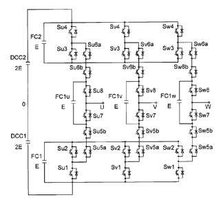
[0002.] FIG. 29 shows a circuit configuration diagram
showing a multilevel power conversion device in a patent
document 1. By setting a phase voltage reference point to
a terminal 0, controlling direct current voltage sources
DCC1 and DCC2 to 2E, and controlling flying capacitors FC1
and FC2 to E, it is possible to output a phase voltage of
five levels of 2E, E, 0,-E, and -2E from output terminals U,
V, and W.
[0003.] Besides, in FIG. 29, maximum voltages applied
to switching elements Sul to Su8, Svl to 5v8, and Swl to
Sw8, and diode elements 5u9 to Su12, Sv9 to Sv12, and
Sw9 to Sw12 in a steady state are E. For equalizing these
maximum applying voltages of all the switching elements
and the diode elements, Su6b and Su8 are connected in
series to each other. This is also applied to the switching
elements Su7 and Su5b, Sv6b and Sv8, Sv7 and Sv5b,
Sw6b and Sw8, Sw7 and Sw5b, Su9 and Sul0, Su11 and
Su12, Sv9 and Sv10, Sv11 and Sv12, Sw9 and Sw10, and
Swll and Sw12.
CA 02920079 2016-02-01
2
[0004.] Moreover, there is proposed a multilevel power
conversion device shown in FIG. 30. In the circuits shown
in FIG. 29 and FIG. 30, used direct current voltage sources
DCC1 and DCC2, and flying capacitors FC1 and FC2 are
common to the three phases. With this, the number of the
capacitors are decreased, and the size of the device is
decreased.
Prior Art Document
Patent Document
[0005.] Patent Document 1: Japanese Patent Application
Publication No. 2013-132261
Summary of The Invention
[0006.] The circuit of FIG. 29 can output phase voltages
of 5 levels. One phase is constituted by ten switching
elements and four diode elements. When three-phases
DC/AC convertor is considered in FIG. 29, the number of
the used switching elements is 30. The number of the
diode elements is 12. The number of the summation is 42.
In this way, in the conventional multilevel power
conversion device, the number of the used elements are
many. The cost of the device is high. The size of the
device is increased.
[0007.] The multilevel power conversion device shown in
FIG. 30 can arbitrarily select charge and discharge patterns
of common flying capacitors, irrespective of outputted
phase voltage levels. However, elements other than the
direct current voltage sources DCC1 and DCC2, and the
flying capacitors FC1 and FC2 are independently used in the
respective phases. Accordingly, the number of the
switching elements are many. The cost of the device is
CA 02920079 2016-02-01
3
high. The size of the device is large. For example, 5 level
power conversion device of the three phases needs 48
switching elements in the three phases.
[0008.] Moreover, by providing the switching elements
Si and S2 which are common to the M phases as shown in
FIG. 31, it is possible to decrease the total number of the
used switching elements. However, it is not possible to
arbitrarily select the charge and discharge patterns of the
flying capacitors FC1 and FC2 which are common to the
respective phases.
[0009.] FIG. 32 shows switching patterns of the output
phase voltage levels E and -E. FIG. 33 shows an example
of a charge and discharge pattern which cannot be
arbitrarily selected in the flying capacitor FC2. In this case,
0 in the drawing represents a switching element which is
conducted (turned on).
[0010.] As shown in FIG. 32, the output phase voltage
levels E and -E have, respectively, two pattern output
methods. In the pattern of E, it is possible to charge and
discharge the flying capacitor FC2. In the pattern of -E, it
is possible to charge and discharge the flying capacitor FC1.
[0011.] However, in a case where the patterns of FIGS.
32(b) and (d) are simultaneously used when the U phase is
E, the V phase is 0, and the W phase is -E as shown in FIG.
33, the switching elements 5u4, Su14, and Si are
simultaneously conducted with each other. Accordingly,
the direct current power source DCC2 and the flying
capacitor FC2 are short-circuited.
4
[0012.] Accordingly, for outputting E to avoid the short-circuit of
the
direct current voltage source DCC2 and the flying capacitor FC2, the
output pattern of FIG. 32(b) cannot be applied. It is limited to the
output pattern of FIG. 32(a). In this way, in a case where the pattern
of the charge and the discharge is limited, it is not possible to
arbitrarily switch the charge and the discharge of the flying capacitors
FC1 and FC2. The control method is complicated.
[0013.] It is, therefore, an object of the present invention to
provide
a multiphase multilevel power conversion device devised to decrease a
number of used elements, and to decrease a cost and a size of the
device.
[0014.] The present invention was devised in consideration of the
above-described conventional problems. According to an aspect of the
present invention, there is provided a multilevel power conversion
device configured to generate an alternating current output which is
converted from voltages of N direct current voltage sources, flying
capacitors, and other capacitors, to a plurality of voltage levels, N being
1, the multilevel power conversion device comprising:
the N direct current voltage sources which are connected in series
with each other, and which are common to all phases;
the flying capacitors including:
a first flying capacitor which has one end connected to a
negative electrode terminal of the series connection of the direct
current voltage sources, and which is common to all phases; and
a second flying capacitor which has one end connected to a
positive electrode terminal of the series connection of the direct current
voltage sources, and which is common to the all phases; and
phase modules of M phases, M being > 2, each of the M phases
including:
CA 2920079 2017-08-03
5
a positive electrode terminal and a negative electrode
terminal of the first flying capacitor, and a positive electrode terminal
and a negative electrode terminal of the second flying capacitor serving
as input terminals;
one end of each one of switching elements being connected
to one of the input terminals,
other ends of adjacent two of the switching elements being
connected to each other in a first sequence,
one end of one of the switching elements being connected
to a common connection point of the switching elements which have
the other ends connected to each other in a second sequence,
the first sequence and the second sequence being repeated
until a final stage in which a number of the switching elements becomes
two,
two of the switching elements of an output stage being
connected in series between the other ends of the two of the switching
elements of the final stage,
one of the other capacitors being connected in parallel with
the two of the switching elements of the output stage,
a common connection point of the switching elements of
the output stage serving as an output terminal,
each of the phase modules of the M phases being configured
to output, from the output terminal, a potential of one of the input
terminals, or a potential obtained by adding or subtracting the voltage
of the one of the other capacitors to or from the potential of the one of
the input terminals, by selectively controlling the respective switching
elements in an ON/OFF manner.
According to a preferred aspect, a multilevel power conversion device
configured to generate an alternating current output which is converted
CA 2920079 2017-08-03
6
to a plurality of voltage levels from voltages of a direct current voltage
source, a flying capacitor, and a capacitor, the multilevel power
conversion device comprising:
the N (1\12) direct current voltage sources which are connected
in series with each other, and which are common to respective phases;
a first flying capacitor which has one end connected to a negative
electrode terminal of each of the direct current voltage sources, and
which are common to the respective phases;
a second flying capacitor which has one end connected to a
positive electrode terminal of each of the direct current voltage
sources, and which are common to the respective phases; and
a phase module of a M phase (1µ,12) including;
a positive electrode terminal and a negative electrode
terminal of the first flying capacitor, and a positive electrode terminal
and a negative electrode terminal of the second flying capacitor being
set to an input terminal;
one end of each of switching elements being connected to
each of the input terminal,
other ends of adjacent two of the switching elements being
connected to each other,
these being repeated until a final stage in which a number
of the switching elements becomes two,
two of the switching elements of an output stage being
connected in series between the other ends of the two of the switching
elements of the final stage,
a capacitor being connected in parallel with the two of the
switching elements of the output stage,
a common connection point of the switching elements of the
output stage being set to an output terminal,
CA 2920079 2017-08-03
7
the phase module of a M phase (M?2) being configured to output,
from the output terminal, a potential of one of the input terminals, or
a potential obtained by adding or subtracting the voltage of the
capacitor to or from the potential of the one of the input terminals, by
selectively controlling the respective switching elements in an ON/OFF
manner.
[0015.]
According to another aspect of the invention, there is
provided a multilevel power conversion device configured to generate
an alternating current output which is converted from voltages of N
direct current voltage sources, flying capacitors, and other capacitors,
to a plurality of voltage levels, N being
2, the multilevel power
conversion device comprising:
the N direct current voltage sources which are connected in series
with each other, and which are common to all phases;
the flying capacitors including:
a first flying capacitor having a positive electrode terminal
connected to a common connection point between a nth direct current
voltage source (n: odd number) and a (n+1)th direct current voltage
source (n+1: even number);
a second flying capacitor having a negative electrode terminal
connected to a common connection point between nth direct current
voltage source and (n+1) direct current voltage source; and
phase modules of M phases, M being
2, each of the M phases
including:
the negative electrode terminal of the nth direct current
voltage source, the negative electrode terminal of the first flying
capacitor, the positive electrode terminal of the nth direct current
power source, and the positive electrode terminal of the second flying
capacitor serving as input terminals,
CA 2920079 2017-08-03
,
,
8
one end of each of switching elements being connected to one
of the input terminals,
the other ends of adjacent two of the switching elements being
connected to each other in a first sequence,
one end of one of the switching elements being connected to
a common connection point between the switching elements which have
the other ends connected to each other in a second sequence,
the first sequence and the second sequence being repeated
until a final stage in which a number of the switching elements becomes
two,
two of the switching elements of an output stage being
connected in series with each other between the other ends of two of
the switching elements of the final stage,
one of the other capacitors being connected in parallel with
two of the switching elements of the output stage,
a common connection point of the switching elements of the
output stage serving as an output terminal,
each of the phase modules of the M phases being configured
to output a potential of one of the input terminals, or a potential
obtained by adding or subtracting the voltage of the capacitor to or
from the potential of the one of the input terminals, by selectively
controlling the respective switching elements in an ON-OFF manner.
[0016.]
According to another aspect of the invention, there is
provided a multilevel power conversion device configured to generate
an alternating current output which is converted from voltages of two
direct current voltage sources, 4N flying capacitors, and other
capacitors, to a plurality of voltage levels, N being
1, the multilevel
power conversion device comprising:
CA 2920079 2017-08-03
9
the two direct current voltage sources which are connected to each
other, and which are common to all phases;
the 4N flying capacitors including:
N flying capacitors of first to Nth flying capacitors which have
negative electrode terminals that are connected in order in series with
a negative electrode terminal of the first direct current voltage source,
and which are common to the all phases;
N flying capacitors of (N+1)th to 2Nth flying capacitors which
have positive electrode terminals connected in order in series with a
common connection point between the first direct current voltage
source and the second direct current voltage source, and which are
common to the all phases;
N flying capacitors of (2N+1)th to 3Nth flying capacitors which
have negative electrode terminals connected in order in series with the
common connection point between the first direct current voltage
source and the second direct current voltage source, and which are
common to the all phases, and
N flying capacitors of 4Nth to (3N+1)th flying capacitors which
have positive electrode terminals connected in order in series with the
positive electrode terminal of the second direct current voltage source,
and which are common to the all phases; and
phase modules of M phases, M being ?. 2, each of the M phases
including:
a positive electrode terminal and the negative electrode
terminal of the first flying capacitor, positive electrode terminals of the
second to Nth flying capacitors, negative electrode terminals of the
(N+1) to 2Nth flying capacitors, positive electrode terminals of the
(2N+1) to 3Nth flying capacitors, negative electrode terminals of the
(3N+1) to (4N-1) flying capacitors, and the positive electrode terminal
CA 2920079 2017-08-03
10
and a negative electrode terminal of the 4Nth flying capacitor serving
as input terminals,
one ends of the switching elements being connected to the
respective input terminals,
the other ends of adjacent two of the switching elements being
connected to each other in a first sequence,
one end of one of switching elements being connected to a
common connection point between the switching elements which have
the other ends connected to each other in a second sequence,
the first sequence and the second sequence being repeated
until a final stage in which a number of the switching element becomes
two,
two of the switching elements of an output stage being
connected in series with each other between the other ends of the two
of the switching elements of the final stage,
one of the other capacitors being connected in parallel to the
two of the switching elements of the output stage,
a common connection point of the switching elements of the
output stage serving as an output terminal,
each of the phase modules of the M phases (M2) which are
configured to output, from the output terminal, a potential of one of
the input terminals, or a potential obtained by adding or subtracting a
voltage of the capacitor to or from the potential of the input terminals,
by selectively controlling the switching elements in an ON-OFF manner.
[0017.]
According to another aspect of the invention, there is
provided a multilevel power conversion device configured to generate
an alternating current output which is converted from voltages of two
direct current voltage sources, 2N flying capacitors, and other
CA 2920079 2017-08-03
,
s
11
capacitors, to a plurality of voltage levels, M being ? 2, the multilevel
power conversion device comprising:
the two direct current voltage sources which are connected in
series with each other, and which are common to all phases;
the 2N flying capacitors including:
N flying capacitors of first to Nth flying capacitors which have
negative electrode terminals connected in order in series with the
negative electrode side of the first direct current voltage sources, and
which are common to the all phases, and
N flying capacitors of (N+1) to 2Nth flying capacitors which
have positive electrode terminals connected in order in series with a
positive electrode side of the second direct current voltage source, and
which are common to the all phases;
phase modules of M phases, M being ?. 2, each of the M phases
including:
a positive electrode terminal and the negative electrode
terminal of the first flying capacitor, positive electrode terminals of the
second to Nth flying capacitors, negative electrode terminals of (N+1)th
to (2N-1)th flying capacitors, and the positive electrode terminal and a
negative electrode terminal of the 2N flying capacitor serving as input
terminals,
one end of the switching elements being connected to the
respective input terminals,
the other ends of adjacent two of the switching elements being
connected to each other in a first sequence,
one end of one of switching elements being connected to a
common connection point between the switching elements which have
the other ends connected to each other in a second sequence,
CA 2920079 2017-08-03
12
the first sequence and the second sequence being repeated
until a final stage in which a number of the switching elements becomes
two,
two of the switching elements of an output stage being
connected in series with each other between the other ends of the two
of the switching elements of the final stage,
one of the other capacitors being connected in parallel with
the two of the switching elements of the output stage,
a common connection point of the switching elements of the
output stage serving as an output terminal,
each of the phase modules of the M phases (M?2) being configured
to output a potential of one of the input terminals, or a potential
obtained by adding a voltage of the capacitor to or from the potential
of the one of the input terminals, by selectively controlling the
switching elements in an ON-OFF manner.
[0018.] Preferably, the first direct current voltage source and the
second direct current voltage source are integrated to one direct
current voltage source.
According to another aspect of the present invention, there is provided
a multilevel power conversion device configured to generate an
alternating current output which is converted from a direct current
voltage to a plurality of voltage levels, the multilevel power conversion
device comprising:
N direct current voltage sources which are connected in series with
each other, and which are common to all phases, M being 2;
a basic cell being common to the all phases, and including a first
semiconductor element having one end connected to positive electrode
terminals of the direct current power sources, a second semiconductor
element having one end connected to negative electrode terminals of
CA 2920079 2017-08-03
,
13
the direct current power sources, a flying capacitor connected between
the other end of the first semiconductor element and the other end of
the second semiconductor element, and third and fourth semiconductor
elements connected in series between the common connection point of
the first semiconductor element and the flying capacitor, and the
common connection point of the second semiconductor element and the
flying capacitor; and
phase modules of M phases, M being
2, each of the M phases
including:
at least one of the one end of the first semiconductor element
and the one end of the second semiconductor element, and a common
connection point of the third and fourth semiconductor elements
serving as input terminals,
switching elements disposed between the respective input
terminals and an output terminal,
the phase modules being configured to selectively control the
respective switching elements in an ON-OFF manner,
wherein in each of the phase modules,
one end of one of the switching elements is connected to the
respective input terminals,
the other ends of adjacent two of the switching elements are
connected to each other in a first sequence,
one end of one of the switching elements is connected to a common
connection point between the switching elements which have the other
ends that are connected to each other in a second sequence,
the first sequence and the second sequence are repeated until a
final stage in which a number of the switching elements becomes two,
CA 2920079 2017-08-03
14
two of the switching elements of an output stage are connected in
series between the other ends of the two of the switching elements of
the final stage,
a capacitor is connected in parallel with the two of the switching
elements of the output stage,
a common connection point between the switching elements of the
output stage serves as the output terminal; and each of the phase
modules is configured to output, from the output terminal, a potential
of one of the terminals of the input terminals, or a potential obtained
by adding or subtracting a voltage of the capacitor to or from a potential
of one of the input terminals.
According to another aspect of the present invention, there is provided
a multilevel power conversion device configured to generate an
alternating current output which is converted from a direct current
voltage to a plurality of voltage levels, the multilevel power conversion
device comprising:
N direct current voltage sources which are connected in series with
each other, and which are common to all phases, M being 2;
a basic cell being common to the all phases, and including a first
semiconductor element having one end connected to positive electrode
terminals of the direct current power sources, a second semiconductor
element having one end connected to negative electrode terminals of
the direct current power sources, a flying capacitor connected between
the other end of the first semiconductor element and the other end of
the second semiconductor element, and third and fourth semiconductor
elements connected in series between a common connection point of
the first semiconductor element and the flying capacitor, and a common
connection point of the second semiconductor element and the flying
capacitor; and
CA 2920079 2017-08-03
,
,
phase modules of M phases, M being
3, each of the M phases
including:
at least one of the one end of the first semiconductor element
and the one end of the second semiconductor element, and a common
connection point of the third and fourth semiconductor elements
serving as input terminals,
switching elements which include first to fifth switching
elements, and which are disposed between the respective input
terminals and an output terminal,
10 each of the phase modules being configured to selectively control
the respective first to fifth switching elements in an ON-OFF manner,
wherein in each of the phase modules,
one end of the first switching element is connected to one of the
one end of the first semiconductor element and the one end of the
second semiconductor element,
one end of the second switching element is connected to the
common connection point between the third and fourth semiconductor
elements,
the other ends of the first and second switching elements are
connected to each other,
one end of the third switching element is connected to a common
connection point between the first and second switching elements,
the other end of the third switching element is connected to one
end of a direct current circuit in which the fourth switching element and
the fifth switching element are connected in series with each other,
a cathode of a first diode and an anode of a second diode are
connected to the other of the one end of the first semiconductor
element and the one end of the second semiconductor element,
CA 2920079 2017-08-03
16
the direct current circuit in which the fourth switching element and
the fifth switching element are connected in series with each other is
connected in parallel to the first diode and the second diode,
a common connection point between the fourth and fifth switching
elements is set to an output terminal, or
one end of one of the switching elements is connected to a common
connection point between the fourth and fifth switching elements,
the other ends of adjacent two of the switching elements are
connected to each other in a first sequence,
one of the switching elements is connected to a common
connection point between the switching elements having the other ends
that are connected to each other in a second sequence,
the first sequence and the second sequence are repeated until an
output stage in which a number of the switching elements becomes two,
a common connection point of the two of the switching elements
of the output stage serves as an output terminal;
each of the phase modules is configured to output, from the output
terminal, a potential of one of the input terminals, by selectively
controlling the respective switching elements in an ON-OFF manner.
According to another aspect of the present invention, there is provided
a multilevel power conversion device configured to generate an
alternating current output which is converted from a direct current
voltage to a plurality of voltage levels, the multilevel power conversion
device comprising:
a first direct current voltage source which is common to all phases;
a second direct current voltage source which is common to the all
phases, and which has a negative electrode terminal connected to a
positive electrode terminal of the first direct current voltage source;
and
CA 2920079 2017-08-03
17
a first basic cell being common to the all phases, and including a
first semiconductor element having one end connected to the positive
electrode terminal of the first direct current voltage source, a second
semiconductor element having one end connected to the a negative
electrode terminal of the first direct current voltage source, a flying
capacitor connected between the other end of the first semiconductor
element and the other end of the second semiconductor element, and
third and fourth semiconductor elements connected in order in series
with each other between a common connection point of the first
semiconductor element and the flying capacitor, and a common
connection point between the second semiconductor element and the
flying capacitor;
a second basic cell being common to the all phases, and including
a first semiconductor element having one end connected to a positive
electrode terminal of the second direct current voltage source, a second
semiconductor element having one end connected to the negative
electrode terminal of the second direct current voltage source, a flying
capacitor connected between the other end of the first semiconductor
element and the other end of the second semiconductor element, and
third and fourth semiconductor elements connected in order in series
with each other between a common connection point between the first
semiconductor element and the flying capacitor, and a common
connection point between the second semiconductor element and the
flying capacitor;
phase modules of M phases, M being ?. 3, each of the M phases
including:
the one end of the second semiconductor element of the first
basic cell, a common connection point of the third and fourth
semiconductor elements of the first basic cell, a common connection
CA 2920079 2017-08-03
18
point between the first semiconductor element of the first basic cell and
the second semiconductor element of the second basic cell, a common
connection point of the third and fourth semiconductor elements of the
second basic cell, and the one end of the first semiconductor element
of the second basic cell serving as input terminals,
first and second switching elements on a side of the second
basic cell being connected in order in series with each other between
the one end of the first semiconductor element of the second basic cell
and the common connection point of the third and fourth semiconductor
elements of the second basic cell,
first and second switching elements on a side of the first basic
cell being connected in order in series with each other between the one
end of the second semiconductor element of the first basic cell, and the
common connection point of the third and fourth semiconductor
elements of the first basic cell,
one end of a third switching element on the side of the first
basic cell being connected to the common connection points of the first
and second switching elements on the side of the first basic cell,
one end of the third switching element on the side of the
second basic cell being connected to the common connection point of
the first and second switching elements on the side of the second basic
cell,
fifth and fourth switching elements being connected in order
in series between the other end of the third switching element on the
side of the second basic cell, and the other end of the third switching
element on the side of the first basic cell,
a cathode of a first diode and an anode of a second diode being
connected to the common connection point of the one end of the first
CA 2920079 2017-08-03
18a
semiconductor element of the first basic cell, and the one end of the
second semiconductor element of the second basic cell,
a direct current circuit in which the fourth switching element
and the fifth switching element are connected in series with each other
being connected parallel to the first diode and the second diode,
a common connection point of the fourth and fifth switching
elements serving as an output terminal,
each of the phase modules of the M phases (r/13) being configured
to selectively control the respective switching elements in an ON-OFF
manner,
each of the phase modules being configured to output a potential
of one of the input terminals from the output terminal by selectively
controlling the respective switching elements in the ON-OFF manner.
According to the present invention, there is also provided a multilevel
power conversion device configured to generate an alternating current
output which is converted from a direct current voltage to a plurality
of voltage levels, the multilevel power conversion device comprising:
N direct current voltage sources which are connected in series with
each other, and which are common to all phases, N being ..?_ 2;
a basic cell being common to the all phases, and including a first
semiconductor element having one end connected to positive electrode
terminals of the respective direct current power sources, a second
semiconductor element having one end connected to negative electrode
terminals of the direct current power sources, a flying capacitor
connected between the other end of the first semiconductor element
and the other end of the second semiconductor element, and third and
fourth semiconductor elements connected in series between a common
connection point of the first semiconductor element and the flying
CA 2920079 2017-08-03
I 8b
capacitor, and a common connection point of the second semiconductor
element and the flying capacitor; and
phase modules of M phases, M being _?. 3, each of the M phases
including:
at least one of the one end of the first semiconductor element
and the one end of the second semiconductor element, and a common
connection point of the third and fourth semiconductor elements
serving as input terminals,
switching elements which include first to third switching
elements, and which are disposed between the respective input
terminals and an output terminal,
each of the phase modules being configured to selectively control
the respective switching elements in an ON-OFF manner,
wherein in each of the phase modules,
one end of the first switching element is connected to one of the
one end of the first semiconductor element and the one end of the
second semiconductor element,
one end of the second switching element is connected to a common
connection point between the third and fourth semiconductor elements,
the other ends of the first and second switching elements are
connected to each other,
one end of the third switching element is connected to the common
connection point between the first and second switching elements,
one end of a bidirectional switch is connected to the other of the
one end of the first semiconductor element and the one end of the
second semiconductor element,
the other end of the third switching element is connected to the
other end of the bidirectional switch,
CA 2920079 2017-08-03
18c
a common connection point between the third switching element
and the bidirectional switch is set to the output terminal,
each of the phase modules is configured to output a potential of
one of the input terminals from the output terminal, by selectively
controlling the respective switching elements.
Preferred embodiments are described hereunder.
[0019.] According to a preferred aspect, a multilevel power
conversion device configured to generate an alternating current output
which is converted to a plurality of voltage levels from voltages of a
direct current voltage source, a flying and a capacitor, the multilevel
power conversion device comprising:
2N+2 direct current voltage sources (N?.1) which are connected
in series with each other, and which are common to respective phases;
a phase module of a M phase (M?_2) including;
positive electrode terminals and negative electrode
terminals of first and (2N+2)th direct current voltage sources, positive
electrode terminals of second to Nth direct current voltage sources, and
negative electrode terminals of (N+3)th to (2N+1)th direct current
voltage sources being set to input terminals,
one end of the switching element being connected to the
respective input terminals,
the other ends of adjacent two of the switching elements
being connected to each other,
one end of the switching element being connected to a
common connection point between the switching elements having the
other ends connected to each other,
these being repeated until a final stage in which a number
of the switching elements becomes two,
CA 2920079 2017-08-03
,
18d
two of the switching elements of the output stage being
connected in series with each other between the other ends of two of
the switching elements of the final stage,
a capacitor being connected in parallel with the two of the
switching elements of the output stage,
the common connection point between the switching
elements of the output stage being set to the output terminal,
the phase module of M phases (M2) configured to output a
potential of one of the input terminals, or a potential obtained by adding
a voltage of the capacitor to or from the potential of the one of the
input terminals, by selectively controlling the switching elements in an
ON-OFF manner.
[0020.]
Preferably, the (N+1)th direct current voltage source and the
(N+2)th direct current voltage source are integrated to one direct
current voltage source.
[0021.] According to a preferred aspect, a multilevel power
conversion device configured to generate an alternating current output
which is converted to a plurality of voltage levels from a direct current
voltage, the multilevel power conversion device comprising:
N direct current voltage sources (N.2) which are connected in
series with each other, and which are common to respective phases;
a basic cell including a first semiconductor element having one
end connected to positive electrode terminals of the respective direct
current power sources, a second semiconductor element having one end
connected to negative electrode terminals of the second direct current
power source, a flying capacitor connected between the other end of
the first semiconductor element and the other end of the semiconductor
element, and third and fourth semiconductor elements connected in
series between the common connection point of the first semiconductor
CA 2920079 2017-08-03
,
,
18e
element and the flying capacitor, and the common connection point of
the second semiconductor element and the flying capacitor; and
a phase module of M phases (M?3) including;
at least one of the one end of the first semiconductor
element and the one end of the second semiconductor element, and a
common connection point of the third and fourth semiconductor
elements being set to input terminals,
a switching element disposed between the respective input
terminals and the output terminal,
the phase module being configured to selectively control the
respective switching elements in an ON-OFF manner.
[0022.] According to a preferred aspect, in the phase module, one
end of the switching element is connected to the respective input
terminals,
the other ends of the adjacent two of the switching elements are
connected to each other,
one end of the switching element is connected to a common
connection point between the switching elements which have the other
ends that are connected to each other,
these sequences are repeated until a final stage in which a
number of the switching elements becomes two,
the two switching elements of the output stage are connected in
series between the other ends of the two of the switching elements of
the final stage,
the capacitor is connected in parallel with two of the switching
elements of the output stage,
a common connection point between the switching elements of
the output stage is set to the output terminal; and the phase module
is configured to output, from an output terminal, a potential of one of
CA 2920079 2017-08-03
18f
the terminals of the input terminals, or a potential obtained by adding
or subtracting a voltage of the capacitor to or from a potential of one
of the input terminals.
[0023.] According to a preferred aspect, in the phase module,
one end of the first switching element is connected to one of one
end of the first semiconductor element and one end of the second
semiconductor element,
one end of the second switching element is connected to a
common connection point between the third and fourth semiconductor
element,
the other ends of the first and second switching elements are
connected to each other,
one end of the third switching element is connected to a common
connection point between the first and second switching elements,
one end of a direct current circuit in which the fourth switching
element and the fifth switching element are connected in series with
each other,
a cathode of a first diode and an anode of a second diode are
connected to the other of the common connection point between the
one end of the first semiconductor element and the one end of the
second semiconductor element,
a direct current circuit in which the fourth switching element and
the fifth switching element are connected in series with each other is
connected in parallel to the first diode and the second diode,
a common connection point between the fourth and fifth
switching elements is set to an output terminal, or the one end of the
switching element is connected to the common connection point
between the fourth and fifth switching elements,
CA 2920079 2017-08-03
18g
the other ends of adjacent two of the switching elements are
connected to each other,
the switching element is connected to a common connection
point between the switching elements having the other ends that are
connected to each other,
this is repeated until an output stage in which a number of the
switching elements becomes two,
the common connection point of the two switching elements of
the output stage is set to an output terminal;
the phase module is configured to output, from the output
terminal, a potential of one of the input terminals, by selectively
controlling the respective switching elements in an ON-OFF manner.
[0024.] According to a preferred aspect, in the phase module,
one end of the first switching element is connected to one of one
end of the first semiconductor element and one end of the second
semiconductor element,
one end of the second switching element is connected to a
common connection point between the third and fourth semiconductor
elements,
the other ends of the first and second switching elements are
connected to each other,
one end of the third switching element is connected to the
common connection point between the first and second switching
elements,
one end of a bidirectional switch is connected to a common
connection point of the other of the one end of the first semiconductor
element and the one end of the second semiconductor element,
CA 2920079 2017-08-03
,
18h
the common connection point between the third switching
element and the bidirectional switch is connected to the output
terminal,
the phase module is configured to output a potential of one of
the input terminals from the output terminal, by selectively controlling
the respective switching elements.
[0025.] According to a preferred aspect, two switching elements are
connected in series between the other ends of adjacent two of the
switching elements which are other than the final stage,
the capacitor is connected in parallel with the two switching
elements which are connected in series with each other,
one end of the switching element of a next stage is connected to
a common connection point of the two switching elements which are
connected in series with each other;
a potential of one of the input terminals, or a potential obtained
by adding or subtracting a voltage of a capacitor connected in parallel
with the switching element of the output stage, and a voltage of a
capacitor connected in parallel with the switching element connected in
series between adjacent two of the switching elements which are other
than the final stage by selectively controlling the respective switching
elements in an ON-OFF manner is outputted from the output terminal.
[0026.] Preferably,
the respective direct current voltage sources are
divided into two or more direct current connections.
[0027.] Preferably, a
part or all of the switching elements and the
semiconductor elements are divided into two or more direct current
connections. A part or all of the switching elements and the
semiconductor elements are divided into two or more parallel current
connections.
CA 2920079 2017-08-03
,
18i
[0028.] In the multiphase multilevel power conversion device
according to the present invention, it is possible to decrease the
number of the used elements, and to decrease the cost and the size of
the device.
Brief Description of Drawings
[0029.]
FIGS. 1 are schematic views showing a pattern at 0 output in
a conventional circuit.
FIG. 2 is a circuit configuration view showing a multilevel power
conversion device according to a first embodiment.
FIGS. 3 are schematic views showing examples of operations at
each output voltage in the first embodiment.
FIG. 4 is a circuit configuration view showing a multilevel power
conversion device according to a second embodiment.
FIGS. 5 are schematic views showing an example of operations
at each output voltage in the second embodiment.
FIG. 6 is a circuit configuration view showing a multilevel power
conversion device according to a third embodiment.
FIG. 7 is a circuit configuration view showing a multilevel power
conversion device according to a fourth embodiment.
CA 2920079 2017-08-03
CA 02920079 2016-02-01
19
FIG. 8 is a circuit configuration view showing a
multilevel power conversion device according to a fifth
embodiment.
FIG. 9 is a circuit configuration view showing a
multilevel power conversion device according to a sixth
embodiment.
FIG. 10 is a circuit configuration view showing a
multilevel power conversion device according to a seventh
embodiment.
FIG. 11 is a circuit configuration view showing a
multilevel power conversion device according to an eighth
embodiment.
FIG. 12 is a circuit configuration view showing a
multilevel power conversion device according to a ninth
embodiment.
FIGS. 13 are schematic views showing phase modules.
FIG. 14 is a circuit configuration view showing a
multilevel power conversion device according to a tenth
embodiment.
FIG. 15 is a circuit configuration view showing a
multilevel power conversion device according to an
eleventh embodiment.
FIG. 16 is a circuit configuration view showing a
multilevel power conversion device according to a twelfth
embodiment.
FIG. 17 is a circuit configuration view showing a
multilevel power conversion device according to a
thirteenth embodiment.
FIG. 18 is a circuit configuration diagram showing a
structure of a basic cell.
,
CA 02920079 2016-02-01
,
FIG. 19 is a circuit configuration diagram showing a
circuit in which the basic cells are connected in series to
each other.
FIG. 20 is a circuit configuration view showing a
5 multilevel power conversion device according to a
fourteenth embodiment.
FIGS. 21 are schematic views showing switching
patterns of the basic cell.
FIGS. 22 are schematic views showing switching
10 patterns at respective voltages of the multilevel power
conversion device according to the fourteenth embodiment.
FIG. 23 is a circuit configuration view showing a
multilevel power conversion device according to a fifteenth
embodiment.
15 FIGS. 24 are schematic views showing switching
patterns at respective voltages of the multilevel power
conversion device according to the fifteenth embodiment.
FIG. 25 is a circuit configuration view showing a
multilevel power conversion device according to a sixteenth
20 embodiment.
FIGS. 26 are schematic views showing switching
patterns at respective voltages of the multilevel power
conversion device according to the sixteenth embodiment.
FIG. 27 is a block diagram showing a multilevel power
conversion device according to the sixteenth embodiment.
FIGS. 28 are a schematic diagram showing a phase
module.
FIG. 29 is a circuit configuration view showing one
example of a conventional multilevel power conversion
device.
CA 02920079 2016-02-01
,
21
FIG. 30 is a circuit configuration view showing another
example of a conventional multilevel power conversion
device.
FIG. 31 is a circuit configuration view showing still
another example of a conventional multilevel power
conversion device.
FIGS. 32 are schematic views showing switching
patterns of the output phase voltages E and -E of the
conventional multilevel power conversion device.
FIG. 33 is a schematic view showing a switching
pattern which cannot be selected.
Description of Embodiments
[0030.] Hereinafter, first to seventeenth embodiments of
multilevel power conversion devices according to the
present invention are illustrated in detail with reference to
FIG. 1 to 28.
[0031.] [First Embodiment]
FIG. 1 shows an example of a pattern in which a
phase voltage 0 is outputted in a conventional art shown in
FIG. 29. In the conventional art shown in FIG. 29, the
phase voltage 0 is outputted by using diode elements Su9
to Su12. However, these diode elements Su9 to Su12 can
be omitted if it is possible to output the phase voltage 0 by
other means.
[0032.] In this first embodiment, as shown in FIG. 2, the
diode elements Su9 to Su12, Sv9 to Sv12, and Sw9 to
Sw12 are omitted by connecting new (newly-added) flying
capacitors FC1, FC1v, and FC1w to respective phases. With
this, the number of the elements are reduced.
CA 02920079 2016-02-01
,
22
[0033.] Hereinafter, a circuit diagram of the multilevel
power conversion device according to the first embodiment
is illustrated with reference to FIG. 2. The multilevel
power conversion device according to the first embodiment
includes direct current voltage sources DCC1 and DCC2,
and flying capacitors FC1 and FC2 which are common to the
respective phases. By the phase modules provided to the
respective phases, the voltage is selected, and outputted
from output terminals U, V, and W. The phase module
includes switching elements Sul to Su8, and a capacitor
FClu in the U phase.
[0034.] Hereinafter, a concrete circuit diagram of the U
phase is illustrated as an example. A direct current voltage
source (a direct current capacitor or a direct current power
source) DCC1 and DCC2 are connected in series with each
other. A common connection point (neutral point) between
the direct current voltage source DCC1 and DCC2 is set to
a terminal 0.
[0035.] A negative electrode terminal of the flying
capacitor FC1 which is common to the respective phase is
connected to a negative electrode terminal of the direct
current voltage source DCC1. A positive electrode terminal
of the flying capacitor FC2 is connected to a positive
electrode terminal of the direct current voltage source
DCC2.
[0036.] The positive electrode terminal and negative
electrode terminal of the flying capacitor FC1, and the
positive electrode terminal and the negative electrode
terminal of the flying capacitor FC2 are connected to phase
modules of respective phases, as input terminals.
CA 02920079 2016-02-01
23
[0037.] One ends of the switching elements Sul to Su4
are connected to the input terminals. The other ends of
adjacent switching elements Sul and Su2 are connected
with each other. The other ends of adjacent switching
elements Su3 and Su4 are connected with each other. One
end of the switching elements Su5a is connected to a
common connection point between the adjacent switching
elements Sul and Su2. One end of the switching element
Su6a is connected to a common connection point between
the adjacent switching elements Su3 and Su4. The
switching elements Su7 and Su8 of the output stage are
connected in series to each other in order between the
other ends of the switching elements Su5a and Su6a of the
final stage through the switching elements Su5b and Su6tb.
The capacitor FClu is connected in parallel with the
switching elements Su7 and Su8 of the output stage. The
common connection point between the switching elements
Su7 and Su8 of the output stage is the output terminal U.
Besides, the switching elements Su5b and Su6b are
connected in series with the switching elements Su5a and
Su6a for the withstand voltage.
[0038.] By selectively controlling the respective
switching elements of this phase module in an ON-OFF
manner, it is possible to output the potential of one of the
input terminals, or a potential obtained by adding or
subtracting the voltage of the capacitor FClu to or from the
potential of one of the input terminals, from the output
terminal U.
[0039.] Besides, the V phase and W phase are similarly
constructed.
CA 02920079 2016-02-01
24
[0040.] In this circuit structure, by controlling the
voltages of the direct current voltage source DCC1 and
DCC2 to 2E, and by controlling the voltages of the flying
capacitor FC1 and FC2, and the capacitors FClu, FC1v, and
FC1w to E, it is possible to output phase voltages of 5
levels of 2E, E, 0, -E, -2E from the output terminals U, V,
and W. Besides, the reference point of the phase voltage is
the terminal 0. Besides, in a case where a three-phase
DC/AC conversion device is considered, the number of the
used switching elements is 30, and the number of the used
diode elements is 0.
[0041.] By using the capacitors FC1u, FC1v, and FC1w, it
is possible to output 0 voltage from output terminals U, V,
and W. Accordingly, it is possible to omit the diode
elements Su9 to Su12, Sv9 to Sv12, and Sw9 to Sw12 of
the conventional art. It is possible to decrease the number
of the used diode elements by 12, relative to the
conventional circuit diagram shown in FIG. 29.
[0042.] Accordingly, it is possible to decrease the
number of the diode elements to 0 without varying the
number of the switching elements, relative to the circuit
configuration shown in FIG. 29.
[0043.] Typical switching patterns of the U phase is
shown in a table 1 and FIG. 3. By switching by the
patterns shown in the table 1, it is possible to output the
phase voltages of the 5 levels of 2E, E, 0, -E, -2E. 0 in
figure shows a switching element which is conducted.
[0044.] [Table 1]
Su4 Su6a 5u6b Su8 Su7 SuSb SuSa Sul Su3 Su2 you
ON ON ON ON OFF OFF OFF OFF OFF OFF 2E -
OFF ON ON ON OFF OFF OFF OFF ON OFF E
¨
CA 02920079 2016-02-01
OFF ON ON OFF ON OFF OFF OFF ON OFF 0
OFF OFF OFF OFF ON ON ON OFF OFF ON -E
OFF OFF OFF OFF ON ON ON ON OFF OFF -2E
[0045.] The voltages applied to the flying capacitors are
illustrated. In the patterns of (2) and (3) of FIG. 3, the
flying capacitor FC2 is charged. Moreover, the capacitor
5 FC1u is charged at the pattern of (3) of FIG. 3.
Furthermore, although it is not shown in FIG. 3, there are a
pattern in which the flying capacitor FC1 is charged, and a
pattern in which the flying capacitor FC1 and FC2, and the
capacitor FC1u is discharged. By performing these charge
10 and discharge, it is possible to control the voltages of the
flying capacitors FC1 and FC2, and the flying capacitor
FC1u to E while the phase voltage is outputted.
[0046.] Besides, in the first embodiment shown in FIG. 2,
the maximum voltages applied to the switching elements in
15 the steady state are E. This is identical to a value of the
conventional art shown in FIG. 29.
[0047.] As described above, in the multilevel power
conversion device according to the first embodiment, it is
possible to decrease the number of the elements.
20 Moreover, it is possible to decrease the cost and the size of
the device.
[0048.] [Second Embodiment]
FIG. 4 shows a circuit configuration of a multilevel
power conversion device according to a second embodiment.
25 The second embodiment has a circuit configuration which is
identical to that of the first embodiment. However, voltage
ratios of the direct current voltage sources DCC1 and DCC2,
the flying capacitors FC1 and FC2, and the capacitors FC1u,
CA 02920079 2016-02-01
26
FC1v, and FC1w are varied. Besides, the reference point of
the phase voltage is the terminal 0.
[0049.] In the second embodiment, the voltages of the
direct current voltage sources DCC1 and DCC2 are
controlled to 2.5E. The voltages of the flying capacitors
FC1 and FC2 are controlled to E. The voltages of the
capacitors FC1u, FC1v, and FC1w are controlled to 2E.
With these, it is possible to output the phase voltage of 6
levels of 2.5E, 1.5E, 0.5E, -0.5E, -1.5E, and -2.5E from the
output terminals U, V, and W. FIG. 5 shows an operation
example and current paths of respective output voltages.
[0050.] In this way, by varying the voltage ratios of the
direct current voltage sources DCC1 and DCC2, and the
flying capacitors FC1 and FC2, and the capacitors FC1u,
FC1v, and FC1w, it is possible to enlarge the number of the
levels relative to the first embodiment. Consequently, it is
possible to increase the number of the levels relative to the
first embodiment while the number of the switching
elements are maintained to the same number. Accordingly,
it is possible to suppress the output voltage and the
harmonic of the current.
[0051.] [Third Embodiment]
FIG. 6 shows a circuit configuration of a multilevel
power conversion device according to the third embodiment.
The multilevel power conversion device of the third
embodiment is provided with direct current voltage sources
DCC1 to DCC4 which are common to the respective phases.
By the phase modules provided to the respective phases,
the voltage is selected, and outputted from the output
terminals U, V, and W. The phase module is provided with
CA 02920079 2016-02-01
27
the switching elements Sul to Su8, and the capacitor FClu
in the U phase.
[0052.] Hereinafter, a concrete circuit configuration of
the U phase is illustrated as an example. The direct
current voltage sources (the current capacitors or the
direct current power sources) DCC1 to DCC4 are connected
in series with each other. A common connection point (a
neutral point) between the direct current voltage sources
DCC2 and DCC3 is set to a terminal 0.
[0053.] The positive and negative electrode terminals of
the direct current voltage source DCC1 and, and the
positive and negative electrode terminals of the direct
current voltage source DCC4 are connected, as the input
terminals, to the phase modules of the respective phases.
[0054.] One ends of the first switching elements Sul to
Su4 are connected to the input terminals. The other ends
of adjacent switching elements Sul and Su2 are connected
to each other. The other ends of adjacent switching
elements Su3 and Su4 are connected to each other. One
ends of the switching elements Su5a and Su6a are
connected to the common connection points of the adjacent
switching element Sul and Su2, and the adjacent switching
element Su3 and Su4. The switching elements Su7 and
Su8 of the output stage are connected in series with each
other in order between the other ends of the switching
elements Su5a and Su6a of the final stage through the
switching elements Su5b and Su6b. The capacitor FClu is
connected in parallel with the switching elements Su7 and
Su8 of the output stage. The common connection point of
CA 02920079 2016-03-31
28
the switching elements Su7 and Su8 of the output stage is
set to the output terminal.
[0055.] By selectively controlling the respective
switching elements of this phase module in an ON-OFF
manner, it is possible to output the potential of one of the
input terminals, or a potential obtained by adding or
subtracting the voltage of the capacitor FC1u to or from the
potential of one of the input terminals, from the output
terminal U.
[0056.] Besides, the V phase and W phase are similarly
constructed.
[0057.] In this circuit configuration, by controlling the
voltages of the direct current voltage sources DCC1 to
DCC4, and by controlling the voltages of the capacitors
FC1u, FC1v, and FC1w to E, it is possible to output the
phase voltages of 5 levels from the output terminals U, V,
and W. Besides, the reference point of the phase voltage is
the terminal 0.
[0058.] In the multilevel power conversion device
according to the third embodiment, it is possible to output
0 from the output terminals U, V, and W by using the flying
capacitors FC1u, FC1v, and FC1w similarly to the first
embodiment. Accordingly, it is possible to omit the diode
elements Su9 to SU12, Sv9 to Sv12, and Sw9 to Sw12 of
the conventional art (FIG. 29). It is possible to decrease
the number of the used diode elements by 12, relative to
the conventional circuit configuration.
[0059.] Besides, the maximum voltages applied to the
switching elements in the steady state are E similarly to
the first embodiment and the second embodiment.
CA 02920079 2016-03-31
29
[0060.] Moreover, it is possible to enlarge the number of
the levels by varying the voltage ratio similarly to the
second embodiment. For example, in a case where the
voltages of the direct current power sources DCC1 and
DCC4 are controlled to E, the voltages of DCC2 and DCC3
are controlled to 1.5E, and the voltages of the capacitors
Fc1u, FC1v, FClw are controlled to 2E, it is possible to
output the phase voltages of 6 levels of 2.5E, 1.5E, 0.5E, -
0.5E, -1.5E, -2.5E.
[0061.] [Fourth Embodiment]
FIG. 7 shows a circuit configuration of a multilevel
power conversion device according to a fourth embodiment.
[0062.] Hereinafter, a circuit configuration of the
multilevel power conversion device according to the fourth
embodiment is illustrated. The multilevel power conversion
device includes direct current voltage sources DCC1 and
DCC2, and the flying capacitors FC1 and FC2 which are in
common to the respective phases. The phase modules
provided to the respective phases selects the voltage, and
outputs from the output terminals U, V, and W. The phase
modules in the U phase includes switching elements Sul to
Su8, and the capacitor FC1u.
[0063.] Hereinafter, a concrete circuit configuration of
the U phase is illustrated as an example. The direct
current voltage sources (the direct current capacitor or the
direct current power source) DCC1 and DCC2 are connected
in series with each other. The common connection point
(the neutral point) of these direct current voltage sources
DCC1 and DCC2 is set to the terminal 0.
CA 02920079 2016-02-01
..
[0064.] The positive electrode terminal of the flying
capacitor FC1 and the negative electrode terminal of the
flying capacitor FC2 are connected to the common
connection point between the direct current voltage source
5 DCC1 and DCC2.
[0065.] The negative electrode terminal of the direct
current voltage source DCC1, the negative electrode
terminal of the flying capacitor FC1, the positive electrode
terminal of the direct current voltage source DCC2, and the
10 positive electrode terminal of the flying capacitor FC2 are
connected, as the input terminals, to the phase modules.
[0066.] One ends of the first switching terminals Sul to
Su4 are connected to the input terminals. The other ends
of the adjacent switching elements Sul and Su2 are
15 connected to each other. The other ends of the adjacent
switching elements Su3 and Su4 are connected with each
other. The one ends of the switching elements Su5a and
Su6a are connected to the common connection points
between the adjacent switching elements Sul and Su2, and
20 the connection points between the adjacent switching
elements 5u3 and Su4. The switching elements 5u7 and
Su8 of the output stage are connected in series in order
between the other ends of the switching elements Su5a and
Su6a of the final stage through the switching elements
25 Su5b and Su6b. The capacitor FClu is connected in
parallel with the switching elements Su7 and Su8 of the
output stage. The common connection point of the
switching elements Su7 and Su8 of the output stage is set
to the output terminal U.
..
CA 02920079 2016-02-01
..
31
[0067.] By selectively controlling the respective
switching elements of this phase module in the ON-OFF
manner, it is possible to output the potential of one of the
input terminals, or the potential obtained by adding or
subtracting the voltage of the capacitor FClu to or from the
potential of one of the terminals, from the output terminal
U.
[0068.] Besides, the V phase and the W phase have
identical configuration.
[0069.] The direct current voltage sources DCC1 and
DCC2 are controlled to 2E. The flying capacitors FC1 and
FC2 are controlled to E. The capacitors FC1u, FC1v, and
FC1w are controlled to E. With these, it is possible to
output the phase voltages of 5 levels of 2E, E, 0, -E, and -
2E. Besides the reference point of the phase voltage is set
to the terminal 0.
[0070.] In the multilevel power conversion device
according to the fourth embodiment, it is possible to output
0 from the output terminals U, V, and W by using the
capacitors FClu, FC1v, and FC1w, similarly to the first
embodiment. Accordingly, it is possible to omit the diode
elements Su9 to Su12, Sv9 to Sv12, and 5w9 to Sw12 of
the conventional art (FIG. 29). It is possible to decrease
the number of the used diode elements by 12 relative to
the conventional circuit configuration of FIG. 29.
[0071.] Besides, the maximum voltages applied to the
switching elements in the steady state are E similarly to
the first and second embodiments.
[0072.] Moreover, it is possible to enlarge the number of
the levels by varying the voltage ratio similarly to the
CA 02920079 2016-03-31
32
second embodiment. For example, in a case where the
voltages of the direct current voltage sources DCC1 and
DCC2 are controlled to 2.5E, the voltages of the flying
capacitors FC1 and FC2 are controlled to 1.5E, and the
voltages of the capacitors FClu, FC1v, FClw are controlled
to 2E, it is possible to output the phase voltages of 6 levels
of 2.5E, 1.5E, 0.5E, -0.5E, -1.5E, and -2.5E.
[0073.] [Fifth Embodiment]
FIG. 8 shows a circuit configuration of a multilevel
power conversion device according to a fifth embodiment.
[0074.] Hereinafter, the circuit configuration of the
multilevel power conversion device according to the fifth
embodiment is illustrated. In the multilevel power
conversion device according to the fifth embodiment, the
flying capacitors FC1 and FC2 which are common to the
respective phases in the multilevel power conversion device
according to the first embodiment are set, respectively, to
two stages. That is, the multilevel power conversion device
includes the direct current voltage sources DCC1 and DCC2,
and the flying capacitors FC1, FC2, FC3, and FC4 which are
common to the respective phases. By the phase modules
provided to the respective phase modules, the voltage is
selected, and outputted from the output terminals U, V,
and W. The phase module includes the switching elements
Sul to Su12, and the flying capacitor FClu in the U phase.
[0075.] Hereinafter, the concrete circuit configuration in
the U phase is illustrated as the example. The direct
current voltage sources (the direct current capacitor or the
direct current power source) DCC1 and DCC2 are connected
in series with each other. The common connection point
CA 02920079 2016-02-01
33
(the neutral point) between the direct current voltage
sources DCC1 and DCC2 is set to the terminal 0.
[0076.] The negative electrode terminal of the flying
capacitor FC1 is connected to the negative electrode
terminal of the direct current voltage source DCC1. The
flying capacitor FC2 is connected in series with the flying
capacitor FC1.
[0077.] The positive electrode terminal of the flying
capacitor FC4 is connected to the positive electrode
terminal of the direct current voltage source DCC2. The
flying capacitor FC3 is connected in series with the flying
capacitor FC4.
[0078.] The positive electrode terminal and the negative
electrode terminal of the flying capacitor FC1, the positive
electrode terminal of the flying capacitor FC2, the negative
electrode terminal of the flying capacitor FC3, and the
positive electrode terminal and the negative electrode
terminal of the flying capacitor FC4 are connected as the
input terminals to the phase modules.
[0079.] One ends of the switching elements Sul to 5u4,
Su6, and 5u7 are connected to the input terminals. The
other ends of the adjacent switching elements Sul and Su2
are connected to each other. The other ends of the
adjacent switching elements Su3 and Su4 are connected to
each other. The one ends of the switching elements Su5
and Su8 are connected to the common connection point of
the adjacent switching elements Sul and Su2, and the
common connection point of the adjacent switching
elements Su3 and Su4. The other ends of the adjacent
switching elements Su5 and Su6 are connected to each
ss
CA 02920079 2016-02-01
e,
34
other. The other ends of the adjacent switching elements
Su7 and Su8 are connected to each other. The one ends of
the switching elements Su9a and Su10a are connected to
the common connection point of the adjacent switching
elements Su5 and Su6, and the common connection point
of the adjacent switching elements Su7 and Su8. The
switching elements Su11 and Su12 of the output stage are
connected in series with each other in order between the
switching elements Su9a and Su10a of the final stage
through the switching elements Su9b and Su1Ob. The
capacitor FC1u is connected in parallel with the switching
elements Su11 and Su12 of the output stage. The common
connection point between the switching elements Su11 and
Su12 of the output stage is the output terminal U.
[0080.] By selectively controlling the respective
switching elements of this phase module in the ON-OFF
manner, it is possible to output the potential of one of the
input terminals, or the potential obtained by adding or
subtracting the voltage of the capacitor FC1u to or from the
potential of one of the input terminals, from the output
terminal U.
[0081.] Besides, the V phase and the W phase have the
identical configuration.
[0082.] In a case where the voltages of the direct
current voltage sources DCC1 and DCC2 are controlled to
3.5E, the voltages of the flying capacitors FC1, FC2, FC3,
and FC4 are controlled to E, and the voltages of the
capacitors FC1u, FC1v, and FC1w are controlled to 2E, it is
possible to output the phase voltages of the 8 levels of
3.5E, 2.5E, 1.5E, 0.5E, -0.5E, -1.5E, -2.5E, and -3.5E from
CA 02920079 2016-02-01
the output terminals U, V, and W. Besides, the reference
point of the phase voltage is the terminal 0.
[0083.] A table 2 shows typical switching patterns in the
fifth embodiment.
5 [0084.] [Table 2]
5u4 5u3 Su8 SulOa SulOb Su12 Su11 Su9b Su9a Su5 Sul S07 Su6 9u2 Ii
ON OFF ON ON ON ON OFF OFF OFF OFF OFF OFF OFF OFF 3.5E
OFF ON ON ON ON ON OFF OFF OFF OFF OFF OFF OFF OFF 2.5E
OFF OFF OFF ON ON ON OFF OFF OFF OFF OFF ON OFF OFF 1.5E
OFF ON ON ON ON OFF ON OFF OFF OFF OFF OFF OFF OFF 0.5E
OFF OFF OFF ON ON OFF ON OFF OFF OFF OFF ON OFF OFF 0.5E
OFF OFF OFF OFF OFF OFF ON ON ON OFF OFF OFF ON OFF -1,5E
OFF OFF OFF OFF OFF OFF ON ON ON ON OFF OFF OFF ON -2,55
OFF OFF OFF OFF OFF OFF ON ON ON ON ON OFF OFF OFF -35E
[0085.] Besides, the maximum voltages applied to the
switching elements in the steady state is E similarly to the
first and second embodiments.
10 [0086.] In this fifth embodiment, the number of the
levels of the phase voltages which can be outputted is
increased. Accordingly, the number of the necessary
switching elements is increased. However, the fifth
embodiment has a configuration in which the flying
15 capacitors which are common to the respective phases in
the first embodiment are constructed as the multistage.
Accordingly, it is possible to decrease the number of the
diode elements without varying the number of the
switching elements, relative to the conventional circuit
20 system which has the same number of the phase voltage
levels. Moreover, the number of the levels is increased.
Accordingly, it is possible to decrease the harmonic
(higher harmonic wave) of the output voltage and the
current, and to decrease the size of the harmonic
25 suppression filter.
[0087.] [Sixth Embodiment]
CA 02920079 2016-02-01
36
FIG. 9 shows a circuit configuration of a multilevel
power conversion device according to the sixth embodiment.
[0088.] Hereinafter, the circuit configuration of the
multilevel power conversion device according to a sixth
embodiment is illustrated. There are provided the direct
current voltage sources DCC1 and DCC2, and the flying
capacitors FC1, FC2, FC3, and FC4 which are common to
the respective phases. By the phase modules provided to
the respective phases, the voltages are selected, and
outputted from the output terminals U, V, and W. The
phase module in the U phase includes the switching
elements Sul to Su12, and the capacitor FClu.
[0089.] Hereinafter, the concrete circuit configuration of
the U phase is illustrated as an example. The direct
current voltage sources (the direct current capacitors or
the direct current power sources) DCC1 and DCC2 are
connected in series with each other. The common
connection point (the neutral point) of these direct current
voltage sources DCC1 and DCC2 is set to a terminal 0.
[0090.] The negative electrode terminal of the flying
capacitor FC1 is connected to the negative electrode
terminal of the direct current voltage source DCC1. The
positive electrode terminal of the flying capacitor FC2 and
the negative electrode terminal of the flying capacitor FC3
are connected to the common connection point between the
direct current voltage source DCC1 and the direct current
voltage source DCC2. The positive electrode terminal of
the flying capacitor FC4 is connected to the positive
electrode terminal of the direct current voltage source
DCC2.
..
CA 02920079 2016-02-01
..
37
[0091.] The positive electrode terminal and the negative
electrode terminal of the flying capacitor FC1, the negative
electrode terminal of the flying capacitor FC2, the positive
electrode terminal of the flying capacitor FC3, and the
positive electrode terminal and the negative electrode
terminal of the flying capacitor FC4 are connected to the
phase modules as the input terminals.
[0092.] One ends of the switching elements Sul to Su4,
Su6, and Su7 are connected to the input terminals. The
other ends of the adjacent switching elements Sul and Su2
are connected with each other. The other ends of the
adjacent switching elements Su3 and Su4 are connected to
each other. The one end of the switching element Su5 is
connected to the common connection point between the
adjacent switching elements Sul and 5u2 . The one end of
the switching element Su8 is connected to the common
connection point between the adjacent switching elements
Su3 and Su4. The other ends of the adjacent switching
elements Su5 and Su6 are connected to each other. The
other ends of the adjacent switching elements Su7 and Su8
are connected to each other. The one end of the switching
element Su9a is connected to the common connection point
between the adjacent switching elements Su5 and Su6.
The one end of the switching element SulOa is connected
to the common connection point between the adjacent
switching elements Su7 and Su8. The switching elements
Su11 and Su12 of the output stage are connected in series
with each other in order between the other ends of the
switching elements Su9a and SulOa of the final stage
through the switching elements Su9b and SulOb. The
s.
CA 02920079 2016-02-01
..
38
capacitor FC1u is connected in parallel with the switching
elements Su11 and Su12 of the output stage. The common
connection point between the switching elements Sul1 and
Su12 of the output stages is set to the output terminal U.
5 [0093.] By selectively controlling the respective
switching elements of this phase module in an ON-OFF
manner, it is possible to output the potential of one of the
input terminals, or a potential obtained by adding or
subtracting the voltage of the capacitor FC1u to or from the
10 potential of one of the input terminals, from the output
terminal U.
[0094.] Besides, the V phase and W phase are similarly
constructed.
[0095.] By controlling the voltages of the direct current
15 voltage sources DCC1 and DCC2 to 3.5E, controlling the
voltages of the flying capacitors FC1 and FC4 to E,
controlling the voltages FC2 and FC3 to 1.5E, and
controlling the voltages the capacitors FC1u, FC1v, and
FClw to 2E, it is possible to output the phase voltages of 8
20 levels of 3.5E, 2.5E, 1.5E, 0.5E, -0.5E, -1.5E, -2.5E, and -
3.5E from the output terminals U, V, and W. Besides, the
reference point of the phase voltage is the terminal 0.
[0096.] In this sixth embodiment, the number of the
levels which can be outputted is increased. Accordingly,
25 the number of the necessary switching elements is
increased. However, the sixth embodiment has a
configuration in which the flying capacitors which are
common to the respective phases in the first embodiment
are varied to the multistage. Accordingly, it is similarly
30 possible to decrease the number of the diode elements
..
CA 02920079 2016-02-01
..
39
without varying the number of the switching elements,
relative to a case in which the conventional configuration of
FIG. 29 is enlarged to the same number of the levels,.
Moreover, the number of the levels is increased.
Accordingly, it is possible to suppress the output voltage
and the current harmonics (higher harmonic wave), and to
decease the size of the harmonics suppression filter,
relative to the first to third embodiments.
[0097.] [Seventh Embodiment]
FIG. 10 shows a circuit configuration of a multilevel
power conversion device according to a seventh
embodiment.
[0098.] Hereinafter, the circuit configuration of the
multilevel power conversion device according to this
seventh embodiment is illustrated. In the multilevel power
conversion device according to the seventh embodiment,
the flying capacitors FC1 and FC32 which are common to
the respective phases in the multilevel power conversion
device according to the first embodiment is varied to a four
stages of FC1, FC2, FC3, and FC4. That is, the multilevel
power conversion device includes the direct current voltage
sources DCC1 and DCC2, and the flying capacitors FC1, FC2,
FC3, and FC4 which are common to the respective phase.
By the phase modules provided to the respective phases,
the voltages are selected, and outputted from the output
terminals U, V, and W. The phase module of U phase
includes the switching elements Sul to Su16, and the
capacitors FClu.
[0099.] Hereinafter, a concrete circuit configuration of U
phase is illustrated as an example. The direct current
..
CA 02920079 2016-02-01
..
voltage sources (the direct current capacitors or the direct
current power sources) DCC1 and DCC2 are connected in
series with each other. The common connection point (the
neutral point) between these direct current voltage sources
5 DCC1 and DCC2 is set to the terminal 0.
[0100.] The negative electrode of the flying capacitor
FC1 is connected to the negative electrode terminal of the
direct current voltage source DCC1. The positive electrode
terminal of the flying capacitor FC2 is connected to the
10 positive electrode terminal of the direct current voltage
source DCC1. The negative electrode terminal of the flying
capacitor FC3 is connected to the negative electrode
terminal of the direct current voltage source DCC2. The
positive electrode terminal of the flying capacitor FC4 is
15 connected to the positive electrode terminal of the direct
current voltage source DCC2.
[0101.] The phase modules uses the positive electrode
terminals and the negative electrode terminals of the flying
capacitors FC1 to FC4 as the input terminals.
20 [0102.] The one ends of the first switching elements Sul
to 5u8 are connected to the respective input terminals.
The other ends of the adjacent switching elements Sul and
Su2 are connected with each other. The other ends of the
adjacent switching elements Su3 and Su4 are connected
25 with each other. The other ends of the adjacent switching
elements Su5 and Su6 are connected with each other. The
other ends of the adjacent switching elements Su7 and Su8
are connected with each other. The one ends of the
switching elements Su9 to Su12 are connected to the
30 common connection point of the adjacent switching
..
CA 02920079 2016-02-01
..
41
elements Sul and Su2, the adjacent switching elements
Su3 and Su4, the adjacent switching elements Su5 and Su6,
and the adjacent switching elements Su7 and Su8. The
other ends of the adjacent switching elements Su9 and
Sul are connected with each other. The other ends of the
adjacent switching elements Sun and Su12 are connected
with each other. The switching elements Su13 and Su14
are connected with the common connection point between
the adjacent switching elements Su9 and Sul0, and the
common connection point between the adjacent switching
elements Su11 and Su12. The switching elements Su15
and Su16 of the output stage are connected in series with
in order between the other ends of the switching elements
Su13 and Su14 of the final stage. The capacitor FClu is
connected in parallel with the switching elements Su15 and
Su16 of the output stage. The common connection point
between the switching elements Su15 and Su16 of the
output stage is set to the output terminal U.
[0103.] By selectively controlling the respective
switching elements of this phase module in the ON-OFF
manner, it is possible to output the potential of one of the
input terminals, or the potential obtained by adding or
subtracting the voltage of the capacitor FClu to or from the
potential of the one of the input terminals, from the output
terminal U.
[0104.] Besides, the V phase and the W phase are
similarly constituted.
[0105.] By controlling the voltages of the direct current
voltage sources DCC1 and DCC2 to 4E, controlling the
voltages of the flying capacitors FC1, FC2, FC3, and FC4 to
CA 02920079 2016-02-01
42
E, and controlling the voltages of the capacitors FClu, FC1v,
and FClw to E, it is possible to output the phase voltages
of 9 levels of 4E, 3E, 2E, 1E, 0, -1E, -2E, -3E, and -4E from
the output terminals U, V, and W. Besides, the reference
point of the phase voltage is set to 0.
[0106.] A table 3 shows a typical switching pattern in
this seventh embodiment.
[0107.] [Table 3]
Sui3 Sul2 Su14 Su16 SONS Su13 Su9 Sul Su7 Su11 Su6 Su5 Su4 Su3 Sul Su2 U
ON ON ON ON OFF OFF OFF OFF OFF OFF OFF OFF OFF OFF OFF OFF 4E
OFF ON ON ON OFF OFF OFF OFF ON OFF OFF OFF OFF OFF OFF OFF 3E
OFF ON ON OFF ON OFF OFF OFF ON OFF OFF OFF OFF OFF OFF OFF 2E
OFF OFF ON ON OFF OFF OFF OFF OFF ON ON OFF OFF OFF OFF OFF E
OFF OFF ON ON OFF OFF OFF OFF OFF ON OFF ON OFF OFF OFF OFF 0
OFF OFF OFF OFF ON ON OFF OFF OFF OFF OFF OFF OFF ON ON OFF E
OFF OFF OFF ON OFF ON ON OFF OFF OFF OFF OFF OFF OFF OFF ON 2E
OFF OFF OFF OFF ON ON ON OFF OFF OFF OFF OFF OFF OFF OFF ON -3E
OFF OFF OFF OFF ON ON ON ON OFF OFF OFF OFF OFF OFF OFF OFF -4E
[0108.] In the seventh embodiment, the number of the
levels which can be outputted is increased. Accordingly,
the number of the necessary switching elements are
increased. However, the seventh embodiment has a
configuration in which the fling capacitors which are
common to the respective phases in the first embodiment
are varied to the multistage. Accordingly, it is similarly
possible to decrease the number of the diode elements
without varying the number of the switching elements,
relative to a case in which FIG. 29 of the conventional
configuration is enlarged to the same number of the levels.
Moreover, the number of the levels is increased.
Accordingly, it is possible to suppress the output voltage
and the current harmonics, and to decrease the size of the
..
CA 02920079 2016-02-01
..
43
harmonic suppression filter, relative to the first to third
embodiments.
[0109.] [Eighth Embodiment]
FIG. 11 shows a circuit configuration of a multilevel
power conversion device according to an eighth
embodiment.
[0110.] Hereinafter, the circuit configuration of the
multilevel power conversion device according to the eighth
embodiment is illustrated. In the multilevel power
conversion device according to the eighth embodiment,
switching elements Su17, Su18, Su19, and Su20 are
disposed between the switching elements Su9 and Su10,
and Su11 and Su12 in the multilevel power conversion
device according to the seventh embodiment. A capacitor
FC3u is connected in parallel with the switching elements
Su17 and Su18. A capacitor FC2u is connected in parallel
with the switching elements Su19 and Su20. The one ends
of the switching elements Su13 and Su14 of the next stage
are connected to the common connection point between the
switching elements Su17 and Su18, and the common
connection point between the switching elements Su19 and
Su20. That is, in the eighth embodiment, there is provided
a parallel connection circuit of the switching element and
the capacitor, in addition to the switching element of the
final stage.
[0111.] In the phase module, by selectively controlling
the respective switching elements in the ON-OFF manner,
the potential of one of the input terminals, or the potential
obtained by adding or subtracting the voltages of the
,s
CA 02920079 2016-02-01
44
capacitors FClu, FC2u, and FC3u to or from the potential of
one of the input terminals is outputted.
[0112.] Besides, the V phase and the W phase are
similarly constituted.
[0113.] By controlling the voltages of the direct current
voltage sources DCC1 and DCC2 to 5E, controlling the
voltages of the flying capacitors FC1, FC2, FC3, and FC4 to
E, and controlling the voltages of the capacitors FClu, FC2u,
FC3u, FC1v, FC2v, FC3v, FC1w, FC2w, and FC3w to E, it is
possible to output the phase voltages of 11 levels of 5E, 4E,
3E, 2E, E, 0, -E, -2E, -3E, -4E, and -5E. Besides, the
reference point of the phase voltage is set to the terminal 0.
A table 4 shows a typical switching pattern of the U phase.
[0114.] [Table 4]
5 8 Su12 Su20 Su14 Su16 Sul5 5u13 Null Su9 Sul Sul Su19 Null Su6 Su5 5u4 9u3
Null 5u18 Su2 U
ON ON ON ON ON OFF OFF OFF OFF OFF OFF OFF OFF OFF OFF OFF OFF OFF OFF OFF SE
OFF ON ON ON ON OFF OFF OFF OFF OFF ON OFF OFF OFF OFF OFF OFF OFF OFF OFF 4E
OFF ON OFF ON ON OFF OFF OFF OFF OFF ON ON OFF OFF OFF OFF OFF OFF OFF OFF 3E
OFF OFF ON ON ON OFF OFF OFF OFF OFF OFF OFF ON ON OFF OFF OFF OFF OFF OFF 2E
OFF OFF OFF ON ON OFF OFF OFF OFF OFF OFF ON ON ON OFF OFF OFF OFF OFF OFF E
OFF OFF OFF ON OFF OFF OFF OFF OFF OFF OFF ON ON OFF ON OFF OFF OFF OFF OFF 0
OFF OFF OFF OFF OFF ON ON OFF OFF OFF OFF OFF OFF OFF OFF OFF ON ON ON OFF E
OFF OFF OFF OFF OFF ON ON ON OFF OFF OFF OFF OFF OFF OFF OFF ON ON OFF OFF 2E
OFF OFF OFF OFF OFF ON ON OFF ON OFF OFF OFF OFF OFF OFF OFF OFF OFF OFF ON 3E
OFF OFF OFF OFF OFF ON ON ON ON OFF OFF OFF OFF OFF OFF OFF OFF OFF OFF ON 4E
OFF OFF OFF OFF OFF ON ON ON ON ON OFF OFF OFF OFF OFF OFF OFF OFF OFF OFF 5E
[0115.] In the eighth embodiment, the number of the
diode element is 0, similarly to the seventh embodiment.
Moreover, the number of the levels are increased.
Accordingly, relative to the seventh embodiment, it is
possible to suppress the output voltage and the current
higher harmonics wave, and to decrease the size of the
higher harmonics wave filter.
[0116.] [Ninth Embodiment]
%
CA 02920079 2016-02-01
,.
FIG. 12 shows a multilevel power conversion device
according to a ninth embodiment.
[0117.] FIG. 12 is a multilevel power conversion device
in which a circuit of one phase of the multilevel power
5 conversion device according to the first embodiment is
enlarged to M phase and N stage. The stage number N
(N=1, 2, 3 = = .) is the number of the direct connections of
the direct current power sources which are connected in
series with each other. The direct current voltage sources
10 DCC1 to DCCN are connected in series with each other.
[0118.] The negative electrode terminals of the flying
capacitors FC1, FC3, = = ., and FC2N-1 are connected,
respectively, to the negative electrode terminals of this
direct current voltage sources DCC1 to DCCN. The positive
15 electrode terminals of the flying capacitors FC2, FC4, = =
=,
and FC2N are connected to the positive electrode terminals
of the direct current voltage sources DCC1 to DCCN.
[0119.] FIG.13 shows an example of a configuration of a
phase module used in a multilevel power conversion device
20 according to this ninth embodiment. As shown in FIGS.
13(a) to (d), in all of (a) to (d), flying capacitors FCMO of
the respective phases are provided in parallel to the
switching elements of the output stage. FIGS. 13(a) and
(b) show an example of configuration in which the number
25 of the input terminals of the phase module is a multiple of
4. FIGS. 13(c) and (d) shows an example of a
configuration in which the number of the input terminals of
the phase module is an even number except for the
multiple of 4. A difference between FIG. 13(a) and FIG.
30 13(b) and a difference between FIG. 13(c) and FIG. 13(d)
CA 02920079 2016-03-31
46
is to have the capacitors FCM1 to FCMN except for the
capacitor FCMO connected in parallel with the switching
elements of the output stage.
[0120.] As shown in FIG. 12, the circuit of the ninth
embodiment has the 4N of the number of the input
terminals of the phase modules which is the multiple of 4.
Accordingly, FIG. 13(a) or FIG. 13(b) is selected. The
input terminals of the phase module are connected to the
positive or negative electrode terminals of the flying
capacitors FC1 to FC which are common to the respective
phases.
[0121.] Moreover, the number of the level of the phase
voltage is dependent on the sorts (kinds) of the phase
modules which are applied, and the applying voltages of
the direct current voltage sources DCC1 to DCCN,, the flying
capacitors FC1 to FC2N which are common to the respective
phases, and the applying voltages of the respective
capacitors FCMO, FCM1 to FCMN within the phase module.
In a case where the phase module of FIG. 13(b) is used, by
controlling the voltages of the direct current voltage
sources DCC1 to DCCN of FIG. 12 to 4E, and controlling the
flying capacitors FC1 to FC2N and the flying capacitors
FCMO of the phase module of FIG. 13(b) to E, the number
of the levels of the phase voltages becomes (4N+1).
[0122.] The first embodiment is a case in which N=1 and
N=3 are set in the ninth embodiment, and the phase
module of FIG. 13(b) is applied. The seventh embodiment
is a case in which N=2 and M=3 are set in the ninth
embodiment, and the phase module is applied, the voltages
of the direct current voltage sources DCC1 to DCCN of FIG
CA 02920079 2016-03-31
47
12 are controlled to 4E, the voltages of the flying
capacitors FC1 to FC2N of FIG. 12, and the voltage of the
capacitor FCMO of the phase module is controlled to E. The
second embodiment is a case where N=1 and M=3 is set in
the ninth embodiment, where the phase module of FIG.
13(b) is applied, and where the voltages of the direct
current voltage sources DCC1 to DCCN are controlled to 5E,
the voltages of the flying capacitors FC1 to FC2N are
controlled to E, and the voltage of the capacitor FCM0 of
the phase module of FIG. 13 is controlled to 2E. The
eighth embodiment is a case where N=2 and M=3 are set in
the eighth embodiment, where the phase module of FIG.
13(a) is applied, and where the voltages of the direct
current voltage sources DCC1 to DCCN of FIG. 12 are
controlled to 5E, and the voltages of the capacitors FCMO,
FCM1 to FCMN are controlled to E.
[0123.] Besides, the respective direct current sources
DCC1 to DCCN may be divided.
[0124.] [Tenth Embodiment]
FIG. 14 shows a multilevel power conversion device
according to a tenth embodiment.
[0125.] The multilevel power conversion device according
to the tenth embodiment is different in the connection
configuration of the flying capacitors FC1 to FC2N from the
ninth embodiment.
[0126.] 2N is the number of the direct connections in
which the direct current voltage source are connected with
each other. The direct current voltage sources DCC1 to
DCC2N are connected in series. Moreover, the number of
the flying capacitors FC1 to FC2N is 2N. The positive
..
CA 02920079 2016-02-01
..
48
electrode terminals of the first flying capacitors FC1, FC3, =
= =, and FCn-1 are connected to the common connection
points between the respective direct current voltage
sources DCCn (n: odd number) and DCCn+1 (n+1: even
number). The negative electrode terminals of the flying
capacitors FC2, FC4, = = =, and FC2N are connected to the
common connection points between the respective direct
current voltage sources DCCn (n: odd number) and
DCCn+1 (n+1: even number).
[0127.] Accordingly, in the tenth embodiment, the
number of the direct connection of the direct current
voltage sources DCC1 to DCC2N and the number of the
flying capacitors FCC1 to FCC2N which are common to the
respective phases are the even number. Besides, fv12 is
set.
[0128.] The phase module uses, as the input terminals,
the negative electrode terminals of the direct current
voltage sources DCCn (n: odd number), the negative
electrode terminals of the flying capacitors FCn, the
positive electrode terminals of the direct current voltage
sources DCCn+1, and the positive electrode terminals of
the flying capacitors FCn+1.
[0129.] The number of the levels of the phase voltage is
dependent on the sort (kind) of the applied phase module,
and the applying voltages of the direct current voltage
sources DCC1 to DCCN, the flying capacitors FC1 to FC2N
which are common to the respective phases, and the
capacitors of the respective phases within the phase
module. By controlling the voltages of the direct current
voltage sources DCC1 to DCC2N of FIG. 14 to 2E,
..
CA 02920079 2016-02-01
..
49
controlling the voltages of the flying capacitorsFC1 to FC2N
which are common to the respective phases, and the
voltage of the capacitor FCMO of the phase module which
are shown in FIG. 13(b) to E, the number of the levels of
the phase voltages becomes (4N+1).
[0130.] The forth embodiment is a case where N=1 and
M=3 are set in the ninth embodiment, where the phase
module of FIG 13(b)is selected, where the voltages of the
direct current voltage sources DCC1 to DCCN of FIG. 14 are
controlled to 2E, where the voltage of the flying capacitors
FC1 to FC2N are controlled to E, and where the voltage of
the capacitor FCMO of the phase module of FIG. 13 is
controlled to E.
[0131.] Besides, the direct current voltage sources DCC1
to DCC2N may be respectively divided.
[0132.] [Eleventh Embodiment]
FIG. 15 shows a multilevel power conversion device
according to an eleventh embodiment.
[0133.] The direct current voltage sources DCC1 and
DCC2 are connected in series with each other.
[0134.] The connection configuration of the flying
capacitors FC1 to FC4N are different from the ninth
embodiment and the tenth embodiment. The negative
electrode terminals of the flying capacitors FC1 to FCN are
connected in order in series with the negative electrode
terminal of the direct current power source DCC1. The
positive electrode terminals of the flying capacitors FC2N to
FCN+1 are connected in order in series with the common
connection point between the direct current voltage sources
DCC1 and DCC2. The negative electrode terminals of the
CA 02920079 2016-02-01
..
flying capacitors FC2N+1 to FC3N are connected in this
order in series with the common connection point between
the direct current voltage sources DCC1 and DCC2. The
positive electrode terminals of the flying capacitors FC4N to
5 FC3N+1 are connected in order in series with the positive
electrode terminal of the direct current voltage source
DCC2.
[0135.] The phase module uses, as the input terminals,
the positive electrode terminal and the negative electrode
10 terminal of the flying capacitor FC1, the positive electrode
terminals of the flying capacitors FC2 to FCN, the negative
electrode terminals of the flying capacitors FCN+1 to FC2N,
the positive electrode terminals of the flying capacitors
FC2N+1 to FC3N, the negative electrode terminals of the
15 flying capacitors FC3N+1 to FC4N-1, and the positive
electrode terminal and the negative electrode terminal of
the flying capacitor FC4N.
[0136.] 4N is the number of the flying capacitors.
Accordingly, the number of the flying capacitors FC1 to
20 FC4N is multiples of 4 in the first embodiment. Besides,
M2 is set.
[0137.] In the eleventh embodiment, 4N+2 of the
number of the input terminals of the phase module is the
even number which is not the multiples of 4. The phase
25 module shown in FIGS. 13(c) and (d) are applied.
[0138.] Moreover, the number of the levels of the output
phase voltages is dependent on the sorts (kinds) of the
applied phase module, the applying voltages of the direct
current power sources DCC1 to DCC2, the flying capacitors
30 FC1 to FC4N which are common to the respective phases,
..
CA 02920079 2016-02-01
..
51
and the capacitors FCMO, FCM1 to FCMN within the phase
modules.
The sixth embodiment is an example in which N=1 and
M=3 are set in this eleventh embodiment, in which the
phase module of FIG. 13(d) is used, in which the voltages
of the direct current voltage sources DCC1 to DCCN is
controlled to 3.5E, in which the voltages of the flying
capacitors FC1 and FC4N are controlled to E, in which the
voltages of the flying capacitors FC2N and FC2N+1 are
controlled to 1.5 E, and in which the voltages of the
capacitor FCMO of the phase module of FIG. 13 is controlled
to 2E.
[0139.] Besides, the direct current voltage sources DCC1
to DCC2 may be respectively divided.
15 [0140.] [Twelfth Embodiment]
FIG. 16 shows a multilevel power conversion device
according to a twelfth embodiment.
[0141.] The direct current voltage sources DCC1 and
DCC2 are connected in series with each other.
20 [0142.] The twelfth embodiment is a M phase N stage
multilevel conversion device in which the flying capacitors
FC1 to FC2N are common to the M phase. This is different
from the ninth to eleventh embodiments in the connection
configuration of the flying capacitors FC1 to FC2N.
25 [0143.] The negative electrode terminals of the flying
capacitors FC1 to FCN are connected in order in series with
the negative electrode terminal of the direct current
voltage source DCC1. The positive terminals of the flying
capacitors FC2N to FCN+1 are connected in order in series
..
CA 02920079 2016-02-01
..
52
with the positive electrode terminal of the direct current
voltage source DCC2.
[0144.] 2N is the number of the flying capacitors FC1 to
FC2N. Accordingly, in this structure, the number of the
flying capacitors FC1 to FC2N is the even number. Besides,
M_?_2 is set.
[0145.] The phase module uses, as the input terminals,
the positive electrode terminal and the negative electrode
terminal of the flying capacitor FC1, the positive electrode
terminals of the flying capacitors FC2 to FCN, the negative
electrode terminals of the flying capacitors FCN+1 to FC2N-
1, and the positive electrode terminal and the negative
electrode terminal of the flying capacitors FC2N.
[0146.] In this twelfth embodiment, there is a case
where the number (2N+2) of the input terminals of the
phase module does not become the multiples of 4. In a
case where the number (2N+2) of the input terminals of
the phase module is the multiples of 4, the phase module
shown in FIG. 13(a) and (b) are applied. In a case where
the number (2N+2) is the even number which is not the
multiples of 4, the phase modules which corresponds to the
number of the input terminals as shown in FIGS. 13 (c) and
(d) is applied.
[0147.] Moreover, the number of the levels of the phase
voltage is dependent on the sort (kind) of the applied
phase module, and the applying voltages of the direct
current voltage sources DCC1 to DCC2, the flying
capacitors FC1 to FC4N, and the capacitors within the
phase module.
..
CA 02920079 2016-02-01
..
53
[0148.] The fifth embodiment is an example in which the
N=2 and M=3 are set in FIG. 16, in which the phase
module of FIG. 13(d) is used, in which the voltages of the
direct current voltage sources DCC1 to DCCN are controlled
to 3.5E, in which the voltages of the flying capacitors FC1
to FC2N is controlled to E, and in which the voltage of the
capacitor FCMO of the phase module of FIG. 13 is controlled
to 2E.
[0149.] Besides, the direct current voltage sources DCC1
to DCC2 may be respectively divided. Besides, the direct
current voltage sources DCC1 and DCC2 may be integrated
to one direct current voltage source.
[0150.] [Thirteenth Embodiment]
FIG. 17 shows a multilevel power conversion device
according to a thirteenth embodiment.
[0151.] FIG. 17 is a multilevel conversion device (N=1, 2,
3, = = =) in which the direct current voltage sources which
are common in the M phase are divided to (2N+2) number.
That is, the direct current voltage sources DCC1 to
DCC2N+2 are connected in series with each other.
[0152.] The input terminals of the phase modules are
connected to the direct current voltage sources DCC1 to
DCC2N+2. Specifically, the positive electrode terminals
and the negative electrode terminals of the direct current
voltage sources DCC1 and DCC2N+2, the positive electrode
terminals of the direct current voltage source DCC2 to
DCCN, and the negative electrode terminals of the direct
current voltage sources DCCN+3 to DCC2N+1 are used as
the input terminals. That is, the only connection point
between the direct current voltage sources DCCN+1 and
CA 02920079 2016-02-01
µ.
54
DCCN+2 in the common connection points of the direct
current voltage sources is not connected to the phase
module. Besides, fsl2 is set.
[0153.] In the case the thirteenth embodiment, there is
5 a case where the input terminal number 2N+2 of the phase
module does not become the multiples of 4. In a case
where the input terminal number 2N+2 of the phase
module is the multiples of 4, the phase module shown in
FIGS. 13(a) and (b) are applied. In a case where the input
10 terminal number 2N+2 of the phase module is the even
number which is not the multiples of 4, the phase module
which corresponds to the input terminal number as shown
in FIGS. 13(a) and (b).
[0154.] The number of the levels of the phase voltages is
15 dependent on the sorts (kinds) of the applied phase module,
and the applied voltages of the direct current voltage
sources DCC1 to DCC2N+2 and the capacitors within the
phase modules.
[0155.] The third embodiment is an example where N=1
20 and M=3 are set in FIG. 17, where the phase module of FIG.
13(b) is used, where the voltages of the direct current
voltage sources DCC1 to DCC2N are set to E, and where the
voltage of the capacitor FCMO of the phase module of FIG.
13 is controlled to E.
25 [0156.] Besides, the direct current voltage sources DCC1
to DCC2N+2 may be respectively divided. Moreover, the
direct current voltage sources DCCN+1 and DCCN+2 may
be integrated into one direct current voltage source.
[0157.] [Fourteenth Embodiment]
..
CA 02920079 2016-02-01
FIG. 18 shows a basic cell used in multilevel power
conversion devices according to fourteenth to seventeenth
embodiments. The basic cell includes a flying capacitor
FC1 and semiconductor elements (for example, IGBT) Sf1,
5 Sf2, Sf3, and Sf4. These are common in the M phase.
Hereinabove, there are provided the basic cell which is
common in the phases. With this, it is possible to decrease
the number of the used switching elements (including the
semiconductor elements).
10 [0158.] The terminal 3 is connected to the positive
electrode of the direct current voltage source (the capacitor
or the direct current source). The terminal 1 is connected
to the negative electrode of the direct current voltage
source (the capacitor or the direct current power source).
15 The terminal 2 is connected to the phase module. The
phase module is illustrated later.
[0159.] FIG. 19 shows a configuration in which N number
of the basic cells are connected in series with each other.
In this case, N?.2 is set. The direct current voltage source
20 (the capacitor or the direct power source) is connected to
the terminals 2N+1 and 2N-1. The phase module is
connected to the terminal 2N.
[0160.] FIG. 20 shows a circuit configuration of a
multilevel power conversion device according to a
25 fourteenth embodiment in which the basic cells of FIG. 19
are used.
[0161.] Hereinafter, a circuit configuration of a multilevel
power conversion device according to the fourteenth
embodiment is illustrated with reference to FIG. 20. The
30 multilevel power conversion device according to the
,.
CA 02920079 2016-02-01
..
56
fourteenth embodiment includes the direct power sources
DCC1 and DCC2 which are common to the respective
phases, and the first and second basic cells 10a and 10b.
By the phase modules provided to the respective phases,
the voltage is selected, and outputted from the output
terminals U, V, and W.
[0162.] Hereinafter, a concrete circuit configuration of U
phase is illustrated as an example. The direct current
voltage sources (the direct current capacitors or the direct
current power sources) are connected in series with each
other. The common connection point (the neutral point)
between these direct current voltage sources DCC1 and
DCC2 is set to the terminal 0.
[0163.] The first and second basic cells 10a and 10b
include, respectively, semiconductor elements Sf1a and
Sf1b which have one ends connected to the positive
electrode terminals of the respective direct current voltage
sources DCC1 and DCC2; semiconductor elements Sf2a and
Sf2b which have one ends connected to the negative
electrode terminals of the respective direct current voltage
sources DCC1 and DCC2; flying capacitors FC1 and FC2
which are connected between the other ends of the
semiconductor elements Sf1a and Sflb, and the other ends
of the semiconductor elements Sf2a and Sf2b; and
semiconductor elements Sf3a, Sf4a, Sf3b, and Sf4b which
are connected in series between the common connection
points between the semiconductor elements Sf1a and Sf1b
and the flying capacitors FC1 and FC2, and the common
connection points between the semiconductor elements
Sf2a and Sf2b and the flying capacitors FC1 and FC2. The
..
CA 02920079 2016-02-01
57
basic cells 10a and 10b output the voltages of E and -E
levels to the phase modules by switching the semiconductor
elements Sfla and Sflb, and Sf4a and Sf4b, or Sf2a and
Sf2b, and Sf3a and Sf3b to the ON state.
5 [0164.] The one end of the semiconductor element Sf2a,
the common connection point between the semiconductor
element Sf3a and Sf4a, the common connection point
between the semiconductor elements Sf3b and Sf4b, and
the one end of the semiconductor element Sflb are
connected to the respective phase modules as the input
terminals.
[0165.] The one ends of the switching elements Sul to
Su4 are connected to the input terminals. The other ends
of the adjacent switching elements Sul and 5u2, and Su3
and Su4 are connected with each other. The one ends of
the switching elements Su5a and Su6a are connected to the
common connection point between the adjacent switching
elements Sul and Su2, and the common connection point
between the adjacent switching elements Su3 and Su4.
The switching elements Su7 and Su8 of the output stage
are connected in order in series between the other ends of
the switching elements Su5a and Su6a of the final stage
through the switching elements Su5b and Su6b. The
capacitor FClu is connected in parallel to the switching
elements Su7 and Su8 of the output stage. The common
connection point between the switching elements Su7 and
Su8 of the output stage is set to output terminal U.
Besides, the switching elements Su5b and Su6b are
connected in series with the switching elements Su5a and
Su6a for the withstand voltage.
..
CA 02920079 2016-02-01
..
58
[0166.] By selectively controlling the switching elements
of the phase module in the ON-OFF manner, it is possible
to output the potential of one of the input terminals, or the
potential obtained by adding or subtracting the voltage of
5 the capacitor FC1u to or from the potential of the one of
the input terminals from the output terminal U.
[0167.] Besides, the V phase and the W phase are
similarly constituted.
[0168.] In this circuit configuration, by controlling the
10 voltages of the direct current voltage sources DCC1 and
DCC2 to 2E, controlling the voltage of the flying capacitors
FC1 and FC2, and controlling the voltages of the flying
capacitors FC1 and FC2, and the capacitors FClu, FC1v and
FClw to E, it is possible to output the phase voltages of the
15 5 levels of 2E, E, 0, -E, and -2E. FIG. 21 shows a typical
switching patterns of the U phase. 0 in the drawing
represents the semiconductor element and the switching
element which are conducted. By the path shown in FIG.
21, it is possible to output the phase voltages of 5 levels of
20 2E, E, 0, -E, and -2E.
[0169.] In this fourteenth embodiment, it is possible to
decrease the number of the used switching elements
(including the semiconductor elements Sf1a to Sf4a, and
Sflb to Sf4b) to 38. (The number of the switching
25 elements of the conventional circuit of FIG. 30 is 48. The
number of the switching elements of the conventional
circuit of FIG. 30 is 44). Moreover, it is possible to omit
the gate drive circuit for driving the switching elements.
Accordingly, it is possible to attain the low cost.
..
CA 02920079 2016-02-01
..
59
[0170.] Moreover, it is possible to ensure the freedom of
the charge and the discharge, by limiting the voltage levels
of the common connection points between the switching
elements Sf3a and Sf4a, and Sf3b and Sf4b of the basic
cells 10a and 10b to E, -E (the voltage reference point is
the negative electrode terminals of the direct current
voltage sources DCC1 to DCCN). Accordingly, it is possible
to simplify the control.
[0171.] The circuit of FIG. 31 of the conventional art has
a combination of the switching pattern which the direct
current voltage source DCC1 and the flying capacitor FC1,
and the direct current voltage source DCC2 and the flying
capacitor FC2 may be short-circuited. The fourth
embodiment does not have the pattern which are short-
circuited.
[0172.] This is illustrated by using FIG. 22. 0 in the
drawing shows the element which is conducted. The basic
cells 10a and 10b which are common to the respective
phases performs only the switching of two patterns shown
in FIG. 22. Accordingly, even when any voltage levels are
outputted, the semiconductor elements Sfl and Sf2 are not
simultaneously switched to the ON state. Accordingly, the
short-circuit between the direct voltage source DCC2 and
the flying capacitor FC2 is not generated. The connection
patterns of the flying capacitors FC1 and FC2 can be
switched. It is possible to charge and discharge by
switching the current flowing into and out of the flying
capacitors FC1 and FC2 by switching the connection
patterns in accordance with the current. It is understood
..
CA 02920079 2016-02-01
that the freedom of the charge and the discharge of the
flying capacitors FC1 and FC2 is ensured.
[0173.] FIG. 23 shows a circuit configuration of a
multilevel power conversion device according to fifteenth
5 embodiment. Hereinafter, the circuit configuration of the
multilevel power conversion device according to the
fifteenth embodiment is illustrated based on FIG. 23. The
multilevel power conversion device according to the
fifteenth embodiment includes the direct current voltage
10 sources DCC1 and DCC2 which are common to the
respective phases, and the first and second basic cells 10a
and 10b. By the phase modules provided to the respective
phases, the voltage is selected, and outputted from the
output terminals U, V, and W.
15 [0174.] Hereinafter, a concrete circuit configuration of U
phase is illustrated as an example. The connection
between the direct current voltage sources DCC1 and DCC2
and the basic cells 10a and 10b is identical to that of the
fourteenth embodiment.
20 [0175.] The one end of the semiconductor element Sf2a,
the common connection point between the semiconductor
elements Sf3a and Sf4a, the common connection point
between the semiconductor element Sf3b and Sf4b, the one
end of the semiconductor element Sflb, and the common
25 connection point between the semiconductor elements Sf1a
and Sf2b are connected to the phase modules of the
respective phases as the input terminals.
[0176.] In the phase module, the one end of the
switching element Su1a is connected to the one end of the
30 semiconductor element Sf2a, and the switching element
..
CA 02920079 2016-02-01
.-
61
Sulb is connected to the semiconductor element Sflb. The
one end of the switching element Su2a is connected to the
common connection point between the semiconductor
elements Sf3a and Sf4a. The switching element Su2b is
connected to the common connection point between the
semiconductor elements Sf3b and Sf4b.
[0177.] The other ends of the switching elements Sula
and Su2a are connected with each other. The other ends of
the switching elements Sulb and Su2b are connected with
each other. The one ends of the switching elements Su3a
and Su3b are connected with the common connection
points between the switching elements Sula and Su2a, and
Sulb and Su2b.
[0178.] The switching element Su4a is connected to the
other end of the switching element Su3a. The other end of
the switching element Su3b and the switching element
Su5a are connected. In this case, the switching elements
Su4a, Su4b, Su5b, Su5a are connected in series with each
other so as to constitute the direct current circuit.
20 [0179.] A cathode pf a diode Dula and an anode of a
diode Du2a are connected to the common connection point
between the semiconductor element Sfla and the
semiconductor element Sf2b. The direct current circuit in
which the switching elements Su4a, Su4b, Su5b, and Su5a
are connected in series with each other are connected in
parallel with the diode Dula and the diode Du2a. Besides,
the diode Dulb and Du2b, and the switching elements Su4b
and Su5b are connected in series with the diode Dula and
Du2a, and the switching elements Su4a and Su5a for the
withstanding voltage.
s.
CA 02920079 2016-02-01
62
[0180.] The common connection point between the
switching elements between the switching elements Su4b
and Su5b is set to the output terminal. By selectively
controlling the respective switching elements in the ON-OFF
manner, the potential of one of the input terminals is
outputted from the output terminal.
[0181.] Besides, the V phase and the W phase are
similarly constituted.
[0182.] In this circuit configuration, by controlling the
voltages of the direct current voltage sources DCC1 and
DCC2 to 2E, and controlling the voltages of the flying
capacitors FC1 and FC2 to E, it is possible to output the
phase voltages of 5 levels of 2E, E, 0, -E, and -2E from the
output terminals. FIGS. 24 show typical switching patterns
of the U phase. 0 in the drawing is the conducted
semiconductor element, or the conducted switching element.
By the path shown in FIG. 24, it is possible to output the
phase voltage of 5 levels of 2E, E, 0, -E, and -2E.
[0183.] In this fifteenth embodiment, it is possible to
decrease the number of the used switching element
(including the semiconductor elements) to 38. (The
number of the switching elements of the conventional art of
FIG. 30 is 48. The number of the switching elements of the
conventional art of FIG. 31 is 44.) Moreover, it is possible
to omit the gate drive circuit for driving the switching
elements, and thereby to attain the lower cost.
[0184.] By limiting the voltage levels outputted from the
basic cells 10a and 10b to E and -E by using the basic cells
10a and 10b, it is possible to ensure the freedom of the
CA 02920079 2016-02-01
63
charge and the discharge, and thereby to simplify the
control.
[0185.] Moreover, the loss of the common portions
relative to the circuit of FIG. 33 is decreased.
[0186.] [Sixteenth Embodiment]
FIG. 25 shows a circuit configuration of a multilevel
power conversion device according to a sixteenth
embodiment. Hereinafter, the circuit configuration of the
multilevel power conversion device according to the
sixteenth embodiment is illustrated with reference to FIG.
25. The multilevel power conversion device according to
the sixteenth embodiment includes the direct current power
sources DCC1 and DCC2 which are common to the
respective phases; and the first and second basic cells 10a
and 10b. By the phase modules provided to the respective
phases, the voltage is selected, and outputted from the
output terminals U, V, and W.
[0187.] Hereinafter, a concrete circuit configuration of U
phase is illustrated as an example, The connections of the
direct current voltage sources DCC1 and DCC2, and the
basic cells 10a and 10b are identical to those of the
fourteenth embodiment and the fifteenth embodiment.
[0188.] The one end of the semiconductor element Sf2a,
the common connection point between the semiconductor
elements Sf3a and SF4a, the common connection point
between the semiconductor elements Sf3b and Sf4b, the
one end of the semiconductor element Sf1b, and the
common connection point between the semiconductor
elements Sf1a and Sf2b are connected to the phase
..
CA 02920079 2016-02-01
64
modules of the respective phase modules as the input
terminals.
[0189.] In the phase module, the one end of the
switching element Su1a is connected to the one end of the
semiconductor element Sf2a, and the switching element
Su1b is connected to the one end of the semiconductor
element Sf1b. The one end of the switching element Su2a
is connected to the common connection point between the
semiconductor elements Sf3a and Sf4a. The switching
element Su2b is connected to the common connection point
between the semiconductor elements Sf3b and Sf4b.
[0190.] The other ends of the switching elements Su1a
and Su2a, and Sulb and Su2b are connected with each
other. The one ends of the switching elements Su3a and
Su3b are connected to the common connection points
between the switching elements Su1a and Su2a, and Sulb
and Su2b.
[0191.] The one end of the bi-directional switch is
connected to the common connection point between the
semiconductor element Sf1a and the semiconductor
element Sf2b. The other end of the bidirectional switch
and the other ends of the switching elements Su4 and Su5a
are connected. In this sixteenth embodiment, the
switching elements Su4 and Su5 are inversely connected,
so that the bidirectional switch is constituted. By setting
the common connection point between the switching
elements Su3a and Su3b and the bidirectional switch to the
output terminal, and by selectively controlling the
respective switching elements (including the semiconductor
1
CA 02920079 2016-02-01
elements) in the ON-OFF manner, the potential of one of
the input terminals is outputted from the output terminal.
[0192.] Besides, the V phase and the W phase are
similarly constituted.
5 [0193.] In this circuit configuration, by controlling the
voltages of the direct current voltage sources DCC1 and
DCC2 to 2E, and controlling the voltages of the flying
capacitors FC1 and FC2 to E, it is possible to output the
phase voltages of 5 levels of 2E, E, 0, -E, and -2E from the
10 output terminals U, V, and W. FIGS. 26 show typical
switching patterns of the U phase. 0 in the drawing
represents the conducted semiconductor element and the
conducted switching element. By the path shown in FIG.
26, it is possible to output the phase voltage of 5 levels of
15 2E, E, 0, -E, and -2E.
[0194.] In the sixteenth embodiment, it is possible to
decrease the number of the used switching elements
(including the semiconductor elements) to 32. Moreover, it
is possible to omit the gate drive circuit for driving the
20 switching elements, and thereby to decrease the cost.
[0195.] By limiting the voltage levels outputted from the
basic cells 10a and 10b to E and -E by using the basic cells
10a and 10b, it is possible to ensure the freedom of the
charge and the discharge, and thereby to simplify the
25 control.
[0196.] [Seventeenth Embodiment]
FIG. 27 shows a circuit configuration of a multilevel
power conversion deice according to a seventeenth
CA 02920079 2016-02-01
66
embodiment. In this circuit, the flying capacitors FC1 to
FCN are common to the three phase.
[0197.] N direct current voltage sources DCC1 to DCCN
which are common to the respective phases are connected
in series with each other. The multilevel power conversion
device of FIG. 27 is constituted to the M phases and N
stages by using the direct current power sources DCC1 to
DCCN; a circuit which is formed by enlarging the basic cell
of FIG. 18 to the N stages; and the phase modules of the M
phase. Besides, and M?.3 are set. Moreover, the first,
fourth, fifteenth, and sixteenth embodiments are
configurations in which N=2 and M=3 are set in the circuit
of FIG. 27.
[0198.] The one ends of the semiconductor elements
Sf1a to Sfin are connected to the positive electrode
terminals of the direct current power sources DCC1 to
DCCN. The one ends of the semiconductor elements Sf2a
to Sf2n are connected to the negative electrode terminals
of the direct current voltage sources DCC1 to DCCN. The
configuration of the basic cells 10a to 10n are identical to
those of the fourteenth embodiment.
[0199.] The terminals 1, 2, 3, = = =, 2N-1, 2N, and 2N+1
are set to the input terminals of the phase modules.
Besides, the terminal 3 and the terminal 2N-1 may not be
necessarily connected to the respective phase modules.
The fourteenth embodiment is an example in which the
terminal 3 and the terminal 2N-1 of FIG. 27 are not
connected to the phase modules.
[0200.] In this case, by setting the voltages of the direct
current voltage sources DCC1 to DCCN to 2E, and by
CA 02920079 2016-02-01
67
controlling the voltages of the flying capacitors FC1 to FCN
to E, it is possible to output the phase voltages of 2N+1
levels.
[0201.] FIGS.28 show examples of the phase modules.
FIG. 28(a) is identical to FIG. 13(c). FIG. 28(d) is identical
to FIG. 13(d).
[0202.] In FIG. 28(b), the one ends of the switching
elements S1a, S2a, S2b, and Sib are connected to the
terminals 1, 2, 2N, and 2N+1. The other ends of the
adjacent two switching elements S1a and S2a are
connected to each other. The other ends of the adjacent
two switching elements S2b and Sib are connected to each
other. The one end of the switching element S3a is
connected to the common connection point between the
switching elements S1a and S2a whose the other ends are
connected to each other. The one end of the switching
element S3b is connected to the common connection point
between the switching elements S2b and Sib whose the
other ends are connected to each other.
[0203.] The one end of the direct current circuit in which
the switching element 54a and the switching element S5a
are connected in series with each other is connected to the
other end of the switching element S3a. The direct current
circuit in which the switching element S4b and the
switching element S5b are connected to each other is
connected to the other end of the switching element S3b.
[0204.] The cathodes of the diodes D11 and Din, and the
anodes of the diodes D21 and D2n are connected to the
terminals 3 and 2N-1. The direct current circuit in which
the switching elements S4a and S5a are connected in series
CA 02920079 2016-02-01
68
with each other, and the direct current circuits in which
S4b and S5b are connected in series with each other are
connected in parallel with the diodes Dll and D21, and
Din and D2n. The one ends of the switching elements S8
and S7 are connected to the common connection point
between the switching elements S4a and S5a, and the
common connection point between the switching elements
54b and S5b. The other ends of the switching elements S7
and S8 are connected to each other. The common
connection point between the switching elements S7 and 88
is set to the output terminal.
[0205.] In the fifteenth embodiment, the terminal 3 and
the terminal 2N-1 are set to one. The common connection
point between the switching elements S4b and S5b is set to
the output terminal U. For the withstand voltage, the
diodes Dula and Dulb, Du2a and Du2b, Su4a and Su4b,
and Su5a and Su5b are connected in series with each other.
[0206.] In FIG. 28(c), the one ends of the switching
elements Sla and Sib are connected to the terminals 1 and
2N+1. The one ends of the switching elements S2a and
S2b are connected to the terminals 2 and 2N. The other
ends of the switching elements Sla and S2a, and Sib and
S2b are connected to each other. The one ends of the
switching elements 3a and 3b are connected to the common
connection point between the switching elements Sla and
S2a, and Sib and S2b.
[0207.] The one end of the bidirectional switch is
connected to the terminals 3 and 2N-1. The other end of
the bidirectional switch and the other ends of the switching
elements S3a and S3b are connected to each other. The
,
CA 02920079 2016-02-01
69
common connection points between the switching elements
S3a and S3b, and the bidirectional switch are set to the
output terminals. Besides, in the sixteenth embodiment,
the terminals 3 and 2N-1 are set to one.
[0208.] The phase module has a function to select and
connect one of the input terminals 1, 2, = = =, 2N+1 to the
output terminal OUT by the ON/OFF operation of the
switching elements within the phase module.
[0209.] Moreover, as shown in FIG. 27, circuit groups
from the direct current voltage sources DCC1 to DCCN to
the inputs of phase modules of the respective phases (that
is, the direct current voltage sources DCC1 to DCCN and
the basic cells 10a to 10n) are represented as the direct
current voltage groups 1 to N. In FIG. 27, the voltage
levels inputted from one of the direct current voltage group
I. to N to the phase module are three levels of 0, E, and 2E.
(the voltage reference point is the negative electrode
terminal of the direct current voltage sources DCC1 to
DCCN of the direct current voltage group.)
Moreover, the voltage level 2E of one of the direct
current voltage group, and the voltage level 0 of the direct
current voltage group which is upper stage by one from the
one of the direct current voltage group become the same
phase voltage when viewed from the output terminal of the
phase module. In a structure in which there are N stages
direct current voltage groups, as described above, the
portions in which the voltage levels are superimposed with
each other are (N-1) portions. Accordingly, in FIG. 27, it is
possible to output the voltages of (3N-(N-1)) = (2N+1)
levels, to the output terminals OUT1 to OUTM.
CA 02920079 2016-02-01
[0210.] The fourteenth embodiment is an example in
which the phase module of FIG. 28(d) is used. The
fifteenth embodiment is an example in which the phase
module of FIG.28(b) is used. The sixteenth embodiment is
5 an example in which the phase module FIG. 28(c) is used.
The direct current voltage sources in the fourteenth
embodiment to the sixteenth embodiment are N=2.
Accordingly, the number of the levels of the output
voltages is 5 levels.