Note: Descriptions are shown in the official language in which they were submitted.
CA 02920443 2016-02-04
WO 2015/019106
PCT/GB2014/052431
RF Energy Harvester
Field of Invention
This disclosure relates to an apparatus for harvesting RF energy. More
specifically,
but not exclusively, an antenna for receiving ambient RF energy is disclosed.
In
addition, a rectifier forming part of an RF energy harvesting system and the
integration of the rectifier with a power management module is disclosed.
Background to the Invention
Many electrical devices, particularly portable or remote electrical devices
are
powered by batteries. Batteries usually require recharging or replacing on a
regular
basis for continued operation of the electrical device. However, it is not
always
desirable or possible to connect a device to a mains power supply for
recharging, or
easy to gain access to the device for replacing the batteries. Moreover, it
may not be
possible to rely on a battery to perform with 100% reliability over extended
periods
and/or extreme operational/environmental conditions. As such, other means for
powering/charging devices have been explored.
One proposal for obtaining electrical energy for electrical devices is by
means of
energy harvesting at the electrical device. Energy harvesting involves
converting
energy from clean, freely available sources into electrical energy and
represents an
environmentally friendly solution. Commonly used free energy solutions for
powering
electrical devices include solar, thermal and vibrational energy sources. For
example, practical solar harvesters, such as solar panels and solar rectennas,
utilise
photovoltaic cells to convert photons into electrical energy via the
photovoltaic effect.
However, solutions such as solar harvesters are not appropriate for many types
of
remote electrical devices and are also not ideal for use in many geographical
locations.
An alternative proposal is the wireless delivery of electrical power. For
example, high
power RF sources can be used to deliver RF power in a specific frequency band
to
recipient devices. The recipient devices then receive the RF energy and
convert it
into an electrical form, which can be used to power the device. Such systems
can
work efficiently in certain environments. However, such systems rely upon the
presence of high energy RF transmitters, which reduces the overall
attractiveness of
such systems due to the need to install infrastructure, and therefore limits
the number
of possible applications that can use such technology.
1
CA 02920443 2016-02-04
WO 2015/019106
PCT/GB2014/052431
Due to the expanse in the mobile telecommunications industry in recent decades
and
the corresponding increase in ambient RF energy, some research has looked at
whether such ambient RF energy could be harvested. Presently, few practical
energy collection solution for harvesting ambient RF energy have been
reported,
despite the abundance of such energy. One of the key challenges in respect of
harvesting RF energy includes the collection of very low RF power, which can
be as
low as 10 nW. At present, RF energy harvesting does not look to be a viable
option.
There is therefore still a requirement for alternative sources of power for
remote
devices.
Summary of Invention
In accordance with an aspect of the invention there is provided an antenna
apparatus
for use in harvesting ambient radio frequency, RF, energy. The apparatus
comprises
one or more RF antenna components arranged to receive RF energy for producing
electricity. The one or more RF antenna components comprise a plurality of
frequency filtering components, each frequency filtering component being
arranged
to filter a respective frequency band of the received RF energy.
The frequency filtering components may form part of the one or more RF antenna
components. The frequency filtering components may be features formed in or on
the one or more RF antenna components. Filtering characteristics of the
features
may be determined according to the dimensions of the features. The features
may
be formed in or on the one or more RF antenna components at positions
associated
with one or more resonant frequencies of the one or more RF antennas within
which
they are formed.
The respective frequency bands that the plurality of frequency filtering
components
are arranged to filter may be one or more known electromagnetic radiation
frequency
bands. The one or more known electromagnetic radiation frequency bands may
include one or more of GSM900, GSM1800, 3G, and 4G.
One of the one or more RF antenna components may be a circular radiating patch
arranged to receive a first frequency range. A first of the plurality of
frequency
filtering components may be a curved feature formed concentrically in or on
the
2
CA 02920443 2016-02-04
WO 2015/019106
PCT/GB2014/052431
circular radiating patch. The first filtering component may be arranged for
filtering
one or more frequencies within the first frequency range.
The first frequency filtering component may be positioned at a distance from
the
centre of the circular radiating patch of between Ag/12 and Ag/16, between
Ag/6 and A-
g/15 in length, and between Ag/18.5 to Ag/24.2 in width, wherein Ag is a
wavelength at
a centre frequency of the respective frequency band associated with the
respective
frequency filtering component.
A second of the plurality of frequency filtering components may be a curved
feature
formed concentrically in or on the circular radiating patch arranged for
filtering one or
more frequencies within the first frequency range. The one or more frequencies
filtered by the second frequency filtering component may differ to the one or
more
frequencies filtered by the first frequency filtering component.
The second frequency filtering component may be positioned at a distance from
the
centre of the circular radiating patch of between Ag/12 to Ag/24, between
Ag/4.5 to A-
g/5.7 in length, and between Ag/18.5 to Ag/24.2 in width.
One of the one or more RF antenna components may be a ground plane arranged to
define the radiation pattern of the antenna.
One of the plurality of frequency filtering components may be a feature formed
in or
on the ground plane for filtering one or more frequencies within the second
frequency
range. The feature formed in or on the ground plane may be U-shaped.
The feature formed in or on the ground plane may be at a distance from a
nearest
edge of the circular radiating patch of between Ag/5.4 to Ag/8.1, between
Ag/7.4 to A-
/1O.5 in length, and between Ag/15.2 to Ag/24.2 in width.
The RF antenna arrangement may comprise a substrate on which the circular
radiating patch and the ground plane are formed. The RF antenna arrangement
may
comprise a connection portion at one edge of the substrate for connecting the
circular radiating patch and the ground plane to a harvesting circuit. The
circular
radiating patch may join the connection portion via an elongate feed-line. A
length of
the elongate feed-line may be set so that a distance between the circular
radiating
patch and the ground plane defines an output impedance of the antenna. The
3
CA 02920443 2016-02-04
WO 2015/019106
PCT/GB2014/052431
distance between the circular radiating patch and the ground plane may be
Ag/4.8.
The substrate may be flexible.
The plurality of frequency filtering components may be one or more of notches,
grooves, or protrusions.
In accordance with another aspect of the invention there is provided apparatus
comprising a rectifying circuit arranged to convert a variable electrical
signal received
at an input from an associated antenna into a direct current electrical signal
for
supplying to an electrical energy storage unit, the antenna for use in
harvesting
ambient radio frequency, RF, energy. The apparatus also comprises a power
management module having an input arranged to receive the direct current and
control supply of the direct current to the electrical energy storage unit.
The rectifying
circuit comprises a plurality of transmission lines, wherein the input of the
rectifying
circuit and the input of the power management module are connected via the
plurality
of transmission lines. The power management module is arranged at least
partially
within a boundary defined by the plurality of transmission lines.
The plurality of transmission lines may form first and second arms. The first
arm may
connect the input of the rectifying circuit to the input of the power
management
module via a forward biased rectifying device. The second arm may connect the
input of the rectifying circuit to the input of the power management module
via a
reverse biased rectifying device. The first arm may comprise a first
transmission line
that connects the input of the rectifying circuit to the forward biased
rectifying device,
and a second transmission line that connects the forward biased rectifying
device to
the input of the power management module. The first transmission line may be
arranged for impedance matching the rectifier to the associated antenna, and
the
second transmission line may be arranged for impedance matching the rectifying
circuit with the power management module. The first transmission line may have
a
length of between Ag/6.8 and Ag/8.1, wherein Ag is a wavelength at a centre
frequency
of a respective frequency band arranged to be received by the associated
antenna. A
filtering circuit may be connected to the second transmission line. The
filtering circuit
may be a quarter wavelength stub.
The second transmission line may comprise a linking transmission line and an
impedance matching transmission line. The linking transmission line may be
arranged between the rectifying device and the filtering circuit. The linking
4
CA 02920443 2016-02-04
WO 2015/019106
PCT/GB2014/052431
transmission line is arranged to absorb a capacitive reactance associated with
the
rectifying device. The impedance matching transmission line may be arranged
between the filtering circuit and the power management module. The linking
transmission line may have a length of between Ag/4.3 and Ag/5.6. The
impedance
matching transmission line may have a length of between Ag/3.8 and Ag/4.4.
The power management module may be arranged within the rectifying apparatus
with the following characteristics. The power management module may be
connected at a first end to the output of the rectifying circuit. A distance
between a
second end of the power management module and the input of the rectifying
circuit
may be set to be between Ag/2.5 and Ag/5. A distance between a first side of
the
power management module may be set at between Ag/6.5 and Ag/12 from an edge of
the first arm. A distance between a second side of the power management module
may be set at between Ag/9 and Ag/16.4 from an edge of the second arm.
In accordance with a further aspect of the invention there is provided an RF
energy
harvesting system, comprising an antenna as described herein and an apparatus
as
described herein. The RF energy harvesting system may further comprise an
electrical energy storage unit arranged to receive and store electrical energy
from the
power management module of the apparatus.
A rectenna for harvesting ambient RF energy at power levels below 3 pW is
disclosed. The rectenna may comprise an ultra-wide band planer monopole
antenna
operational over the GSM900, GSM1800 and 3G RF frequency bands. The rectenna
may also comprise a full-wave rectifier having a differential voltage output
and
operational input powers below 3 pW.
An ambient RF harvester is presented where efficiencies above 45% are
achievable
at input RF power levels below 3 pW. To achieve this efficiency, a single
multiband
antenna and a full-wave detector may be provided. Such a harvester not only
charges an energy storage unit faster, but is capable of operating in more
locations
and/or with more flexibility in spatial orientation.
A full-wave rectifier is disclosed with differential output and a modified
omnidirectional
disc monopole antenna with harmonic rejection filters. The new harvester
design may
be capable of operating with an efficiency of 45% in locations with lower
available RF
power.
CA 02920443 2016-02-04
WO 2015/019106
PCT/GB2014/052431
A tri-band RF energy harvester is disclosed with an UWB antenna and integrated
harmonic band rejection. A tetra or N-element harvester array may be provided.
Advantageously, a harvester is provided that is capable of providing duty
cycles
higher than 11%for applications requiring up to 1 mW.
A harvester that avoids harmonic re-radiation thereby improving efficiency and
minimizing detection is disclosed. The harvester may achieve this by filtering
the
higher order harmonics such that they are not radiated by the antenna.
Consequently, it is difficult for a dedicated receiver to detect the presence
of the
harvester when covert operation is required.
In addition, a harvester that provides DC-load isolation from higher-order
harmonics
is disclosed. The harvester may achieve this by use of a high frequency
filtering
circuit. For example, quarter wavelength stubs may form part of the rectifier
for
performing such filtering. Such stubs act as short circuits at the fundamental
frequency, thus filtering RF signal from the output. Alternatively, resonant
structures
such as LC tuned circuits can be used to perform such filtering functionality.
A harvester that is capable of 3rd harmonic rejection for all received bands
is
disclosed. Since half-wave rectification produces odd harmonics and full wave
rectification produces even harmonics in the current waveform the high order
harmonics may be filtered at the output by quarter wavelength stubs and by
notches
formed in the antenna.
The antenna may be formed on a substrate having a bend radius 10 x the
thickness
of the antenna substrate. The minimum bend radius may be 8.6 mm.
The substrate thickness may be 790 pm. The metal antenna formed on the
substrate may be 35 pm thick. The metal may be formed of any suitable
conductive
material. For example, the metal antenna may be formed of copper. The
dielectric
properties of the substrate of dielectric constant cr may be 2.33 and loss
tangent tanO
may be 0.0012.
6
CA 02920443 2016-02-04
WO 2015/019106
PCT/GB2014/052431
Brief Description of the Drawings
Exemplary embodiments of the invention shall now be described with reference
to
the drawings in which:
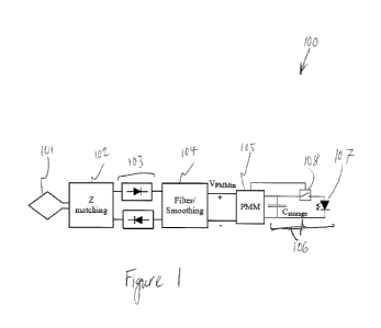
Figure 1 illustrates an RF energy harvesting system;
Figure 2 illustrates a single multi-band antenna used in the system of Figure
1;
Figure 3 illustrates a microstrip full-wave rectifier with a differential
output as
used in the system of Figure 1;
Figure 4 illustrates the rectifier of Figure 4 with the PMM circuit placed
inside
the rectifier;
Figure 5 illustrates an antenna conformed to the surface of a pipe; and
Figure 6 shows an array of antennas conformed to the surface of a pipe.
Throughout the description and the drawings, like reference numerals refer to
like
parts.
Specific Description
A general overview of an RF energy harvesting system shall now be described
with
reference to Figure 1.
A rectenna 100 is shown that includes an antenna 101 arranged to receive
ambient
RF energy. The antenna is designed to receive ambient RF energy across a large
frequency range and therefore the electrical output of the antenna 101 has a
power
profile that fluctuates considerably across its reception frequency range. The
output
of the antenna 101, which provides a variable electrical signal, is connected
to a
rectifier 103 via an impedance matching network 102. The impedance matching
network 102 is provided to minimise losses due to impedance mismatch between
components of the rectenna. The rectifier then converts the received time
varying
electrical signal into a DC electrical signal. The output of the rectifier is
then
smoothed and filtered in a smoothing/filtering circuit 104. This smoothed DC
energy
is then fed into a power management module (PMM) 105 to provide useful
regulated
voltages and charge a storage unit 106, which in this case is a storage
capacitor
Cstorage= The transmission of current to the storage unit 106 and
corresponding
electrical storage in the storage unit 106 is controlled by a power management
module (PMM) 105. The PMM provides maximum power point tracking in addition to
working as a boost converter. The maximum power tracking capabilities of the
PMM
7
CA 02920443 2016-02-04
WO 2015/019106
PCT/GB2014/052431
allow the system to maximize the power transfer to the load by ensuring that
the ideal
load is present across a wide range of input RF power levels. Therefore, the
PMM
also helps to provide a good impedance match with the antenna. The PMM is also
arranged to control a switch 108 that connects the electrical energy stored in
the
storage unit 106 to a load, which in this case is an LED for simplicity of
explanation.
However, in practice the PMM controls the supply of power from the storage
unit 106
to the device, i.e. the load being powered.
The rectenna 100 is designed to maximise the ambient RF energy received by the
antenna 101, and minimise the losses in the conversion of the received energy
to
energy suitable for storing in the storage unit 106. The various components of
the
rectenna 100 shall therefore now be described in detail.
In order to maximise the power harvested by the rectenna and reduce the size
of the
harvester, the antenna 101 is a single multi-band antenna, as can be seen in
Figure
2.
The antenna 101 is a planar antenna structure comprising a substrate upon
which
the receiving components of the antenna are formed. The antenna 101 is a
modified
microstrip disc monopole antenna comprising receiving components including a
circular-shaped radiating patch 110, a feed line 111 and a rectangular shaped
ground
plane 112. The circular-shaped radiating patch 110 and feed line 111 are
arranged
on one side of the substrate, and the ground plane 112 is arranged on the
opposing
side of the substrate. While the antenna is shown as having a microstrip-based
feedline it will be appreciated that a coplanar waveguide feed is provided in
alternative arrangements, or a combination of both a microstrip-based feedline
and a
coplanar waveguide feed. The substrate may be made of any low loss material,
for
example, glass, ceramic, FR4. The planar characteristics of the antenna allow
it to be
formed on the same substrate as the rest of the harvester system.
The antenna 101 is arranged to be substantially omnidirectional in order to
maximise
the received RF radiation. Furthermore, the structural components of the
antenna
are arranged to maximise the receipt of RF energy from different possible
sources.
Since most ambient RF energy comes from mobile telecommunications, the antenna
101 is arranged to operate across an ultra-wide band covering a plurality of
the
following bands: GSM900, GSM1800, 3G, WiFi and 4G. It will be appreciated that
an
alternative antenna arrangement could be arranged to receive other frequency
8
CA 02920443 2016-02-04
WO 2015/019106
PCT/GB2014/052431
bands, higher and lower than those mentioned above to cover radio, TV and
other
ISM bands, if desired. The circular-shaped radiating patch 110 is primarily
arranged
for receiving all bands, while the ground plane 112 is modified to enhance the
3rd
harmonic rejection of specific bands 3G and 4G, which is generated by the
rectification process. The arrangement of the radiating patch 110 and ground
plane
112 for receiving these different frequency bands shall now be discussed in
detail.
The radiating patch 110 is circular in shape and positioned on an upper
portion of the
substrate. An elongated electrical feed line 111 in the form of a microstrip
transmission line provides a connection from the circular-shaped radiating
patch 110
to an end surface of the substrate at point 111a. It is at this point that the
antenna
100 is connectable to the next stage of the energy harvesting system. The
elongate
track 111 not only acts to enable the remainder of the rectenna to be
connected to
the radiating patch 110, but also provides impedance matching, as will be
discussed.
The radius of the disc is a quarter wavelength of the lowest frequency that
the
antenna is arranged to receive, e.g. 945 MHz for GSM900.
The ground plane 112 is rectangular in shape and extends from a bottom of the
antenna substrate to a point just under half way along the length of the
antenna
substrate. In alternative arrangements the ground plane may take a different
form.
The shape of the ground plane defines the impedance and the radiation pattern.
An
electrical connection on an end surface of the substrate allows for the
elongated
track to be electrically connected to the rest of the energy harvesting
system. The
circular-shaped radiating patch, feedline and ground plane are formed of a
conductive material such as copper.
The antenna's impedance can be modified to conjugately match that of the
rectifier
by varying the width of the antenna feed and the distance between the circular-
shaped radiating patch and the ground plane. In particular, the distance
between the
bottom of the circular-shaped radiating patch 110 and the top of the ground
plane
112 can be used to tune the impedance to 50 0 (or any chosen reference
impedance) and optimize the desired omnidirectional pattern. The shape and
overlap of the ground plane with the disc defines the radiation pattern by
reflecting
the field lines coming from the disc. In consequence, this also defines the
gain of the
antenna which can be between 2.3 and 4.8 dBi. This distance is also dependent
upon the wavelengths that the antenna is arranged to receive. In practice the
distance between the bottom of the circular-shaped radiating patch and the top
of the
9
CA 02920443 2016-02-04
WO 2015/019106
PCT/GB2014/052431
ground plane is set between: -Ag/20 and Ag/12.5, where Ag is the guided
wavelength
of the signal at the centre frequency of the selected frequency band. A
distinction of
Ag and Ao is used to highlight that this is the wavelength of the guided-wave
structure, which is different than that in free space.
The antenna 101 has a number of frequency filtering features that are formed
on the
antenna and change the frequency response characteristics of the antenna. In
particular, these filters are arranged to filter out the third harmonic
generated by the
full-wave rectifier at each one of the selected bands that the antenna is
arranged to
receive, e.g. GSM900, GSM1800, and 3G. When the antenna is used with a half-
wave rectifier, a second harmonic filter is required, rather than a third
harmonic filter.
First and second filtering notches 110a and 110b are provided on the circular-
shaped
radiating patch, while a further notch 112a is provided on the ground plane
112. The
first and second notches 110a, 110b are curved and concentrically arranged on
the
circular-shaped radiating patch. The first filtering notch 110a has a length
of Ag/6 to
Ag/7.5. The first filtering notch is radially positioned at between Ag/12 and
Ag/16 from
the centre of the circular-shaped radiating patch. The width of the first
filtering notch
is between Ag/18.5 and Ag/24.2, which optimises the return loss and the
bandwidth of
the notches. The second filtering notch 110b has a length of between Ag/4.5
and
Ag/5.7, a width of between Ag/18.5 and Ag/24.2, and the notch is radially
positioned
Ag/12 to Ag/24 from the centre of the circular-shaped radiating patch. By
modifying
the position and the width of the notches, the return loss can be increased
and the
bandwidth optimized to cover all of the targeted frequencies. It is the
resonances
generated by the position and geometry of the notches that defines the
associated
return loss and bandwidth of the filtering provided by the notches.
The notch 112a formed in the ground plane 112 is U-shaped with the base of the
U
facing downwards. The centre of the notch in the ground plane 112 is between
Ag/5.4 to Ag/8.1 from the lower edge of the circular radiating patch, and the
notch
112a has a length of between Ag/7.4 and Ag/10.5 and a width of between Ag/15.2
and
Ag/24.2.
In summary, the length of the first and second notches is approximately a
third of the
wavelength of the third harmonic and the width is proportional to the
bandwidth
characteristics of the filter. The U-shaped 112a notch is included to filter
the
harmonics created by the 3G rectifier Since there is a different rectifying
circuit for
CA 02920443 2016-02-04
WO 2015/019106
PCT/GB2014/052431
each band, and each rectifier generates third order harmonics corresponding to
their
frequency of operation, different filters or notches are required for each
respective
component of the antenna.
In alternative arrangements additional notches can be added to the structure,
especially in the circular-shaped radiating patch. Additional notches may be
used if
harvesting is also desired at other bandwidths, such as 4G or WiFi. However,
harmonic rejection will be lower than -2 dB. In other words, the additional
filters will
not be able to achieve the desired filtering properties and it is possible
than around
50% of the power in the harmonics will not be filtered.
Figure 3 illustrates the rectifying circuit 103 of Figure 1. The rectifying
circuit 103 is a
microstrip full-wave rectifier with a differential output. The rectifying
circuit shown in
Figure 3 includes the impedance matching 202, rectifier 203, and filtering 104
components shown in the schematic diagram of Figure 1. The rectifying circuit
is
designed to be as lossless as possible to thereby reduce diode voltage drops
resulting of a conventional full-wave (four diode) rectifier. This is
primarily achieved
by ensuring that accurate impedance matching is provided throughout the
circuit.
The rectifier 203 is tuned to the frequency of the frequency range that it is
receiving
form the antenna 101. In the case of the antenna 101, which is arranged to
receive
multiple bands, multiple rectifiers 203 are provided for each respective band.
However, in the Figures only a single rectifier is shown and explained for
ease of
explanation.
The output from the antenna 101 is received at the feed 201 of a microstrip
transmission line. At this point the microstrip transmission line splits into
two arms,
one connecting the input of the rectifier to the output via a forward biased
rectifying
element 203, and a second arm connecting the input of the rectifier to the
output via
a second reverse biased rectifying element 204.
The arms of the microstrip transmission line 202 therefore extend
perpendicularly left
and right from the input 201. The track width of the microstrip transmission
line is set
according to the desired characteristic impedance of the circuit. The track
width can
also be set in order to simplify the impedance matching of the rectifying
circuit with
the antenna. At each end of the impedance matching microstrip transmission
line
202 further parallel tracks run for a short distance perpendicular to the
impedance
matching microstrip transmission line 202 and then each join a first terminal
of a
11
CA 02920443 2016-02-04
WO 2015/019106
PCT/GB2014/052431
respective rectifying element 203, 204. The length of impedance matching
microstrip
transmission line 202 is set so as to match the impedance of the antenna 101,
which
in this case is 50 D. This length is preferably between Ag/6.8 and Ag/8.1.
Hence, the
impedance matching microstrip transmission line is performing the
functionality of the
impedance transformer 102 of Figure 1. The width and length of the microstrip
transmission lines between the input and the rectifying elements are used to
tune the
input impedance of the rectifier.
The rectifying elements are Schottky diodes 203, 204, with the first diode 203
being
forward biased and the second diode 204 being reverse biased. It will be
appreciated that in alternative arrangement a transistor based rectifying
arrangement
may be provided, for example FETs may be modified to perform the rectification
functionality.
The further microstrip transmission line then extends for another short
portion 205,
206 from a second terminal of the respective diode 203, 204. The length and
width
of this part of microstrip line is arranged to absorb the capacitive reactance
of the
diode because they define an inductive reactance. In addition, the length and
width of
this part of the microstrip line can be used in tuning the input impedance of
the
rectifying circuit. The length of the further microstrip transmission line
205, 206 is
preferably between Ag/4.3 and Ag/5.6. At this point, A/4 stubs 207, 208 extend
perpendicularly from the ends of the microstrip transmission lines 205, 206.
The A/4
stubs 207, 208 perform the filtering functionality 104 of Figure 1. The stubs
are used
to filter the fundamental harmonic from the output, providing DC at the
output. The
Ag/4 stub ensures that the fundamental and the higher order harmonics are
below -
45 dBm.
The microstrip transmission line then continues past the stubs for a longer
distance
209, 210, until the two arms of the microstrip transmission line extend
perpendicularly
such that they are again aligned and join at the two output terminals. This
section is
preferably between Ag/3.8 and Ag/4.4 in length. This section works as an
impedance
transformer so that the load and the rest of the rectifier have the conjugate
match of
the antennas' input impedance throughout a range of frequencies and input
power
levels.
In use, diode 203 rectifies the positive part of the received signal and diode
204
rectifies the negative part of the received signal. The quarter wavelength
stubs filter
12
CA 02920443 2016-02-04
WO 2015/019106
PCT/GB2014/052431
the fundamental harmonic from the output ensuring that DC is available. Since
the
output connections are not grounded, the negative voltage coming from the
diode
204 is the reference to the rest of the system blocks, providing a higher
voltage to
reach the cold-start voltage (330 mV) of the PMM.
The output is a differential output, which allows the system to provide a
higher output
voltage VPMM and reach the minimum voltage required by the Power Management
Module (PMM), 330 mV, with input power levels below 3 pW (-25 dBm).
Furthermore, by using a differential output ground vias are avoided, reducing
losses,
helping to achieve a better match between simulations and measurements, as
well
as simplifying fabrication.
A single full-wave rectifier can achieve 12% efficiency at -26 dBm of input
power and
up to 46% at -10 dBm. The return loss is below the -10 dB limit ensuring an
almost
complete cover of the selected operating band. The fractional bandwidth varies
between 2 to 6.2% depending on the operating frequency. The output of the
harvester for the input power range mentioned previously is between, 75 to 550
mV.
In order to minimize the footprint of the complete RF energy harvester, the
PMM
circuit 300 is placed inside a boundary defined by the transmission lines of
the full-
wave rectifier as shown in Figure 4. This is in contrast to known systems
which place
the PMM 300 in series with the rectifier outside the perimeter of the
rectifier.
However, careful considerations are required to avoid coupling between the
rectifying
structure and the miniaturized PMM circuit 300. To minimize the
electromagnetic
interaction between the PMM circuit 300 and the full-wave rectifier the
distance
between the edge of the PMM circuit 300 and the microstrip transmission line
of the
rectifier are set as follows. The PMM circuit 300 joins the differential
output directly.
Hence, the distance between the PMM circuit 300 and the microstrip
transmission
line 211, 212 joining the differential output is negligible. Then, the
distance between
the opposite end of the PMM circuit 300 to the one joining the differential
output and
the input to the rectifying circuit is set to be between Ag/2.5 and Ag/5. A
first side of
the PMM circuit 300 is set at between Ag/6.5 and Ag/12 from a first upper edge
210,
as well as from the second lower edge of the microstrip transmission line and
the
distance between the PMM 300 and the differential output is set at between
Ag/9 and
Ag/16.4.
13
CA 02920443 2016-02-04
WO 2015/019106
PCT/GB2014/052431
In the arrangement shown in Figure 4 the PMM 300 is provided substantially
within
the boundary defined by the transmission lines. It will be appreciated that in
alternative arrangements the PMM may only be provided within some of the
boundary of the transmission line, which would still provide some of the space
savings the energy harvester system as a whole.
In addition to the location of the PMM circuit, the layout shown in Figure 4
avoids the
use of vias, while providing connections for the rectifier's differential
output and the
"grounded" PMM output.
Figure 5 shows how the antenna, and in consequence the rectenna, can conform
to
surfaces. In this case, the substrate on which the antenna 100 is formed is
made
from a flexible material. Consequently, the antenna 100 is bent around a pipe
500.
In this conformal antenna design the pipe 500 is a PVC water pipe with the
following
characteristics: radius = 5 ¨ 10 cm, cr = 2.88, and tan 8 = 0.089. There is no
return
loss degradation from bending the antenna around the pipe.
It will also be appreciated that in an alternative arrangement multiple
antennas may
be provided in an array. For example, Figure 6 shows an array of antennas 100
conformed to a pipe 500. Use of several rectennas increases the total
harvested
power. The distance between each harvester can be as close as Ao/4.8, where Ao
is
the wave-length of the antenna's first resonance.
It will be appreciated that these examples of conforming the antenna to a pipe
are
applicable to any cylindrical object.
It will be appreciated that alternative arrangements could be provided wherein
similar
notches are placed in other types of monopoles and planar antennas such as a
bow-
tie and a square patch. The ground plane could be extended to modify the
radiation
pattern of the antenna. This would also modify the gain of the antenna.
In alternative arrangements multiple filtering components are formed together
as a
filtering arrangement. In other words, as single filtering arrangement is
provided
having multiple filtering components, each filtering component arranged to
perform a
specific filtering functionality such as performing filtering for a specific
frequency
band.
14
CA 02920443 2016-02-04
WO 2015/019106
PCT/GB2014/052431
It will be appreciated that the harvester described herein may be used in
various
applications such as for electronic paper displays, low power displays,
industrial
sensors (e.g. strain-gauge, temperature, pressure, inclination, flow,
proximity, smoke,
gases, C0x, N0x), powering LEDs, and charging storage units.
Furthermore, it will be appreciated that the impedance matching network can be
omitted if the port impedance of the antenna is designed to directly match
that of the
rectifier.
It will be appreciated that the rectifying circuit need not be a microstrip-
based circuit.
For example, in alternative arrangements stripline, coplanar strip or CPW
guided-
wave structures are used. In yet further arrangements lumped-element or lumped-
distributed components are used.
In alternative arrangements the full-wave rectifier can be scaled up or down
in
frequency to any desired frequency band.
In alternative arrangements the antenna is at least one of a bow-tie antenna,
a
modified square patch antenna, dual-monopole antenna, a log-periodic antenna,
a
3D antenna, or a non-planar antenna such as a helical or double-helix antenna.
It will be appreciated that other filtering features such as protrusions could
achieve
the same band filtering response as the notch filter described herein.
Furthermore,
while the notches formed in the circular radiating patch are shown as being
concentric, it will be appreciated that the notches need not be concentric.
However,
improved performance can be achieved by use of concentric notches.
It will be appreciated that the filtering features for different bands may be
provided on
either side of the antenna structure. However, use of a U-notch in the ground
plane
achieves an improved performance for higher frequencies than for lower
frequencies.
The rectenna described above is primarily described for use in harvesting
ambient
RF energy. However, it will be appreciated that the rectenna can also be used
for
receiving RF energy from a dedicated source, or for receiving some RF energy
from
a dedicated source as well as harvesting ambient RF energy.
CA 02920443 2016-02-04
WO 2015/019106
PCT/GB2014/052431
The rectifier described herein is arranged for use with a single frequency
band.
When an antenna is arranged to receive multiple frequency bands a respective
rectifier is utilised for each band.
Where components of the system are shown or described in a way that defines a
particular orientation such as upper or lower, it will be appreciated that the
orientation
is not important but only the relative position(s) of system components.
16