Note: Descriptions are shown in the official language in which they were submitted.
CA 02920726 2016-02-08
WO 2015/023632 PCT/US2014/050646
MULTI-STANDARD LIGHTING CONTROL INTERFACE CIRCUIT
CROSS-REFERENCE TO RELATED APPLICATION
[0001] The present application is an international application which claims
the
benefit of United States Patent Application No. 13/967,385, filed August 15,
2013 and
entitled "MULTI-STANDARD LIGHTING CONTROL INTERFACE CIRCUIT", the
entire contents of which are hereby incorporated by reference.
TECHNICAL FIELD
[0002] The present invention relates to lighting, and more specifically, to
lighting
control interface circuits.
BACKGROUND
[0003] There are a number of lighting control standards currently available
for use
by lighting products. For example, DALI (Digital Addressable Lighting
Interface)
and 0 to 10V are two commonly used lighting control standards. While a DALI
compliant control signal is digital, a 0-10V compliant control signal is
analog. A
DALI interface is bidirectional and is specified in IEC standard 62386. The
high level
of a DALI-compliant control signal is 9.5 to 22.5V (typical 16 V), and the low
level is -
6.5 to 6.5V (typical OV). A lighting control device, such as a ballast or a
solid state
light source driver, as a DALI slave component, may consume only 2.0 mA or
less
from the DALI interface. A DALI interface works with a non-reversed or a
reversed
DALI signal connection. In contrast, a 0-10V control signal is a DC voltage
that
varies between 0 and 10 VDC to produce a varying light intensity level. There
are
two existing 0-10V standards, one of which is for current sourcing controls
and is
supported by the standard ESTA E1.3, Entertainment Technology - Lighting
Control
System - 0-10V Analog Control Protocol, Draft 9 June 1997. The other available
0-
10V standard is for current sink controls, which is specified in IEC standard
60929
Annex E.
1
CA 02920726 2016-02-08
WO 2015/023632 PCT/US2014/050646
SUMMARY
[0004] There are a number of non-trivial issues associated with complying with
the
various available lighting control protocols. For instance, in some cases
where the
lighting control interface is to support multiple standards such as DALI, 0-
10V
(current sink or source), and/or other such lighting protocols, a separate
interface is
required for each such protocol, thereby requiring a distinct or otherwise
dedicated
interface connector for each protocol. Such connectors and the associated
fabrication
costs are relatively expensive and also take up a significant amount of
physical space
per connector. In addition, while some requirements apply to multiple
standards,
other requirements are unique to a given standard and do not apply to other
standards. As such, an interface circuit that works for one standard would not
necessarily be appropriate for another standard.
[0005] Thus, embodiments provide a lighting control interface circuit that
receives
control signals from multiple standards at a common connector (e.g., the same
two
terminals or contact pads of a single connector). The interface circuit
provides a first
protocol output and a second protocol output. These outputs may be digital,
analog
or a combination. For instance, the first protocol output could be an analog
output
for 0-10V compliant signals and the second protocol output could be a digital
output
for DALI compliant signals. A microcontroller unit (MCU) or other suitable
processor receives the various outputs of the interface circuit and recognizes
the
existence of the respective protocols (e.g., DALI digital signal, 0-10V analog
signal,
etc), and then processes the control signal accordingly. The MCU also detects
if no
control signal is connected to the interface circuit. In some embodiments, the
interface circuit includes a common connector operatively coupled to a first
protocol
signal processing section which is in turn operatively coupled to a second
protocol
signal processing section. In such embodiments, the first protocol signal
processing
section effectively passes through a signal having a second protocol. Thus, if
a
second protocol signal is applied to the interface, the MCU/processor will
assess
how that signal manifests at the output of the first protocol signal
processing section
as well as at the output of the second protocol signal processing section, and
is
configured to determine that the output of the second protocol signal
processing
2
CA 02920726 2016-02-08
WO 2015/023632 PCT/US2014/050646
section is the most correct choice and will power a ballast/driver circuit
connected
thereto in accordance with that output/protocol, and will ignore the output of
the
first protocol signal processing section. In a similar fashion, if a first
protocol signal
is applied to the interface, the MCU/processor will assess how that signal
manifests
at the output of the first protocol signal processing section as well as at
the output of
the second protocol signal processing section, and is configured to determine
that
the output of the first protocol signal processing section is the most correct
choice
and that the output of the second protocol signal processing section should be
ignored.
[0006] In some embodiments, the interface circuit is configured to operate
with both
DALI and 0-10V control signals using the same two connectors. In some such
embodiments, the 0-10V protocol section is implemented at the front end of the
interface circuit and is configured with a differential amplifier and a linear
opto-
isolation amplifier to provide the analog 0-10V output and for galvanic
isolation.
The DALI protocol section is implemented at the output of 0-10V protocol
section
and is configured with a translation sub-circuit to provide the digital DALI
output.
The MCU or other processor connected to the respective outputs of the 0-10V
and
DALI protocol sections may recognize the existence of the DALI digital control
signal or the 0-10V analog control signal. Note that any changes made to a
DALI
signal caused by processing through the 0-10V protocol section may be
recognized
and corrected or otherwise compensated for by the processor. The processor may
then process the lighting control signal accordingly.
[0007] In some embodiments, and with respect to recognizing that no control
signal
is connected, the interface circuit may include an on-board signal generator
sub-
circuit configured to apply a signal to the input terminals. In such
embodiments, if
no control signal is connected to the common connector terminals, the output
of the
interface circuit will resemble or otherwise indicate the signal produced by
the signal
generator sub-circuit. On the other hand, if a lighting control signal
complying with
a given protocol is connected to the common connector terminals, the signal
produced by the signal generator sub-circuit is effectively suppressed and the
output
of the interface circuit will resemble or otherwise indicate the protocol of
the applied
3
CA 02920726 2016-02-08
WO 2015/023632 PCT/US2014/050646
lighting control signal. In one such embodiment, for example, a 0-10V lighting
controller that has relatively low output impedance compared to the output
impedance of the signal generator sub-circuit (in some embodiments) is
connected to
the interface. As such, the signal output by the signal generator sub-circuit
is
effectively suppressed by the applied 0-10V control signal. A similar
suppression of
the signal produced by the signal generator sub-circuit occurs if a DALI
lighting
controller is present at the input. An MCU or other processor may be
programmed
or otherwise configured to identify a given control signal type by parameters
indicative of that protocol or the signal output by the signal generator sub-
circuit by
parameters indicative of that signal, and drive the ballast/light circuit
accordingly.
Any one or more standards-based processing sections may be used in conjunction
with such a signal generator sub-circuit, wherein the signal generator sub-
circuit
allows the condition of no control signal at the interface input to be
recognized.
[0008] The interface circuit may be configured with other features or
functionality.
For instance, the interface circuit may also be configured to recognize the
conditions
of input signal polarity reverse and/or signal level. The interface circuit
may also be
configured to withstand a wide voltage range at its input. In some
embodiments,
the interface circuit may withstand voltage between -20 VDC and +20 VDC. The
circuit may also be configured to withstand high AC voltage at its input, such
as 120
VAC. In some embodiments, the interface circuit is configured with an isolated
DC/DC converter and opto-isolation amplifier, so as to provide isolation of
control
signals from AC mains (line and neutral). Numerous other features and
functionality will be apparent in light of this disclosure and may depend on
various
factors such as, for example but not limited to, applicable lighting
standards/protocols, desired lighting performance, and/or existing lighting
infrastructure.
[0009] In an embodiment, there is provided a lighting control interface
circuit. The
lighting control interface circuit includes: an interface connector configured
to
receive a lighting control signal; a control signal processing circuit
operatively
coupled to the interface connector and having a first processing section that
provides
a first output signal at a first output; and a processor configured to receive
the first
4
CA 02920726 2016-02-08
WO 2015/023632 PCT/US2014/050646
output signal via the first output and to determine if a lighting control
signal is being
applied at the interface connector based on the first output signal.
[0010] In a related embodiment, the processor may be further configured to
determine if a lighting control signal applied at the interface connector
complies
with one of a first lighting control protocol and a second lighting control
protocol. In
another related embodiment, the lighting control interface circuit may further
include a signal generator circuit operatively coupled to the interface
connector and
configured to provide a dummy control signal at an output of the control
signal
processing circuit as an indicator to the processor that no lighting control
signal is
currently applied to the interface connector. In a further related embodiment,
the
processor may be further configured to detect the dummy control signal at an
output
of the control signal processing circuit. In another further related
embodiment, a
lighting control signal applied to the interface connector may override the
dummy
control signal. In yet another further related embodiment, the processor may
be
configured to detect the dummy control signal at the first output when no
lighting
control signal is applied to the interface connector.
[0011] In still another related embodiment, the control signal processing
circuit may
further include a second processing section operatively coupled to the first
output
and configured to provide a second output signal at a second output. In a
further
related embodiment, the processor may be further configured to receive the
second
output signal and to determine if the second output signal complies with a
lighting
control protocol in a plurality of lighting control protocols.
[0012] In yet another related embodiment, the first processing section may
include
an isolation amplifier, and the lighting control interface circuit may further
include
an isolated power supply configured to provide power to one side of the
isolation
amplifier. In still another related embodiment, the lighting control interface
circuit
may further include a transmitter communicatively coupled between the
processor
and the interface connector, and configured to allow the processor to
communicate
with a lighting controller connected to the interface connector.
[0013] In another embodiment, there is provided a lighting control interface
circuit.
The lighting control interface circuit includes: an interface connector
configured to
CA 02920726 2016-02-08
WO 2015/023632 PCT/US2014/050646
receive a lighting control signal that is compliant with a lighting control
protocol in a
plurality of lighting control protocols; a control signal processing circuit
operatively
coupled to the interface connector, wherein the control signal processing
circuit
comprises an isolation amplifier configured to provide a first output signal
at a first
output, and a signal translator operatively coupled to the first output and
configured
to provide a second output signal at a second output; and a processor
configured to
receive the first and second output signals and to determine if a lighting
control
signal applied at the interface connector complies with a lighting control
protocol in
the plurality of lighting control protocols.
[0014] In a related embodiment, the lighting control interface circuit may
further
include: a signal generator circuit operatively coupled to the interface
connector and
configured to provide a dummy control signal at an output of the control
signal
processing circuit as an indicator to the processor that no lighting control
signal is
currently applied to the interface connector. In a further related embodiment,
the
processor may be further configured to detect the dummy control signal at an
output
of the control signal processing circuit. In another further related
embodiment, the
processor may be configured to detect the dummy control signal at the first
output
when no lighting control signal is applied to the interface connector.
[0015] In yet another related embodiment, the lighting control interface
circuit may
further include at least one of: an isolated power supply configured to
provide
power to one side of the isolation amplifier; and a transmitter
communicatively
coupled between the processor and the interface connector configured to allow
the
processor to communicate with a lighting controller connected to the interface
connector.
[0016] In another embodiment, there is provided a method of interfacing
lighting
controls. The method includes: receiving a first signal potentially
representative of a
first lighting control signal; receiving a second signal potentially
representative of a
second lighting control signal; and determining if either of the first and
second
signals complies with a first lighting control protocol or a second lighting
control
protocol.
6
CA 02920726 2016-02-08
WO 2015/023632 PCT/US2014/050646
[0017] In a related embodiment, the method may further include: determining
that a
dummy control signal is manifesting in at least one of the first and second
signals,
thereby indicating that no lighting control signal is being applied. In a
further
related embodiment, in response to determining that a dummy control signal is
manifesting in at least one of the first and second signals, the method may
further
include setting output lighting power according to a pre-established value.
[0018] In another related embodiment, in response to determining the first
signal
complies with a first lighting control protocol, the method may further
include
setting output lighting power according to the first lighting control
protocol. In yet
another related embodiment, in response to determining the second signal
complies
with a second lighting control protocol, the method may further include
setting
output lighting power according to the second lighting control protocol.
BRIEF DESCRIPTION OF THE DRAWINGS
[0019] The foregoing and other objects, features and advantages disclosed
herein
will be apparent from the following description of particular embodiments
disclosed
herein, as illustrated in the accompanying drawings in which like reference
characters refer to the same parts throughout the different views. The
drawings are
not necessarily to scale, emphasis instead being placed upon illustrating the
principles disclosed herein.
[0020] FIGs. 1A and 1B each illustrate a block diagram of a lighting control
interface
circuit according to embodiments disclosed herein.
[0021] FIG. 2 illustrates an example configuration of an isolated power supply
of the
lighting control interface circuits of FIGs. 1A and 1B according to
embodiments
disclosed herein.
[0022] FIG. 3 illustrates an example configuration of an amplifier and an
isolation
amplifier of the lighting control interface circuits of FIGs. 1A and 1B
according to
embodiments disclosed herein.
[0023] FIG. 4 illustrates an example configuration of a buffer and a signal
generator
of the lighting control interface circuits of FIGs. 1A and 1B according to
embodiments disclosed herein.
7
CA 02920726 2016-02-08
WO 2015/023632 PCT/US2014/050646
[0024] FIG. 5 illustrates an example configuration of a signal translator of
the
lighting control interface circuits shown in FIGs. 1A and 1B according to
embodiments disclosed herein.
[0025] FIG. 6 illustrates a transmitter of the lighting control interface
circuits of FIGs.
1A and 1B according to embodiments disclosed herein.
[0026] FIG. 7 is a flowchart of methods carried out by one of the lighting
control
interface circuits of FIGs. 1A and 1B according to embodiments disclosed
herein.
DETAILED DESCRIPTION
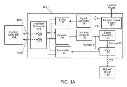
[0027] FIG. 1A illustrates a block diagram of a lighting control interface
circuit 100
(also referred to throughout as an interface circuit 100), which includes an
interface
connector 110, a buffer 112, an amplifier 114, a signal generator 118, an
isolation
amplifier 120, an isolated power supply 122, a signal translator 124, and an
MCU
126. The lighting control interface circuit 100, in some embodiments, is,
after the
interface connector 110, divided into a first protocol section (also referred
to as a
front end and/or front end section) and a second protocol section. The first
protocol
section includes the amplifier 114 and the isolation amplifier 120. The second
protocol section includes the signal translator 124. In some embodiments, one
section or the other includes one or more of the remaining components (i.e.,
the
buffer 112, the signal generator 118, the isolated power supply 122, the
transmitter
116, and/or the MCU 126). In some embodiments, one or more of these components
may be spread across both sections, or in their own section. The interface
circuit 100
is able to receive a control signal (such as but not limited to at least one
of the control
signals 102a, 102b shown in FIG. 1A) from a lighting controller 104. The
interface
circuit 100 determines which one of multiple lighting control protocols
applies to the
received control signal 102a, 102b. Note that regardless of the protocol being
used to
transmit the control signal from the lighting controller 104 to the interface
circuit 100,
the control signal is applied to the same interface connector 110, which in
FIG. 1A
includes two terminals A and B. Though FIG. 1A shows the interface circuit 100
as
working with two protocols, any number of protocols may be, and in some
embodiments are, used, so long as the corresponding protocol of a control
signal
8
CA 02920726 2016-02-08
WO 2015/023632 PCT/US2014/050646
applied at the common interface connector 110 is able to be identified. The
lighting
control interface circuit 100 is also able to detect a no control signal
condition at the
common interface connector 110.
[0028] The isolated power supply 122 provides power to the various sub-
circuits
and/or components of the interface circuit 100. The amplifier 114 is
operatively
connected to the two terminals A and B of the interface connector 110. An
output of
the amplifier 114 is provided to an isolation amplifier 120, which in turn
drives a
signal translator 124. An output signal associated with a first lighting
protocol,
protocol #1 in FIG. 1A, is taken at the output of the isolation amplifier 120,
and an
output signal associated with a second lighting protocol, protocol #2 in FIG.
1A, is
taken at the output of the signal translator 124. An MCU 126 receives both of
these
outputs, evaluates the received signals, and generates an appropriate drive
signal
128. The drive signal 128 is then applied to a ballast/driver 150, which
provides
appropriate power to a lighting circuit connected thereto (not shown in FIG.
1A).
The ballast/driver 150 is any type of ballast and/or driver circuit known in
the art.
The interface circuit 100 also includes the signal generator 118 and the
buffer 112 for
providing a dummy control signal to one or both of the two terminals A and B,
thereby allowing for a no control signal situation to be detected. The
interface circuit
100 also includes an optional transmitter 116 for providing communications
from the
MCU 126 back to the interface connector 110, and specifically back to one or
both of
the two terminals A and B, thereby allowing for bi-directional communication
between the interface connector 110 and the MCU 126, which is used and/or
required by some lighting standards.
[0029] FIG. 1B shows another embodiment of a lighting control interface
circuit 100a
(also referred to throughout as an interface circuit 100a), having some
similar
components to lighting control interface circuit 100 shown in FIG. 1A. In FIG.
1B, the
lighting control interface circuit 100a is integrated directly into a
ballast/driver 150a
and receives signals from a lighting controller 104a, which in some
embodiments is
not integrated with the ballast/driver 150a, and in some embodiments is. Other
such integration schemes will be apparent in light of this disclosure.
Components of
the interface circuit 100 / the interface circuit 100a will now be discussed
in turn.
9
CA 02920726 2016-02-08
WO 2015/023632 PCT/US2014/050646
For ease of description, these components will be discussed in terms of a
first
lighting protocol, i.e., protocol #1 in FIGs. 1A and 1B, being the 0-10V
standard and a
second lighting protocol, i.e. protocol #2 in FIGs. 1A and 1B, being the DALI
standard. In such embodiments, the lighting controller 104 / the lighting
controller
104a may be, for example but not limited to, a 0-10V dimmer, a DALI master
controller, both, or other similar components. Of course, embodiments are not
so
limited and thus may and do use different lighting control protocols and/or
lighting
controller(s). Similarly, the interface connector 110 may be, and in some
embodiments is, any standard or custom interface connector suitable for the
protocols to be supported, and may, and in some embodiments does, include any
number of terminals and/or other contacts needed to communicate the signal(s)
of a
given standard/protocol. As will be appreciated in light of this disclosure,
and in
some embodiments, a control signal compliant with a given one of various
standards
supported by the interface circuit is able to be applied to the same interface
connector 110 as control signals compliant with others of the various
standards,
thereby eliminating the need for multiple interface connectors. Thus, while
the
interface connector 110 shown in FIGs. 1A and 1B includes two terminals A and
B,
other embodiments may and do include an interface connector having any number
of terminals, such as but not limited to a single terminal for +V with a
connector
plug casing for -V, or three terminals that allow for +V, -V, and a dedicated
communication channel, respectively, and so on. Further, the interface
connector
110 may and does take any number of form factors and thus may and does
include,
for example but not limited to, a plug/receptacle arrangement and/or wires
directly
soldered to corresponding conductors on a substrate, such as but not limited
to a
printed wiring board (PWB). The corresponding conductors to which the wires
are
soldered may be, for instance, conductive pads or vias, or conductive runs or
posts.
In some embodiments, the interface connector is configured to wirelessly
receive
lighting control signals, in which embodiments the interface connector
includes
appropriate transmission and reception components, such as but not limited to
an
antenna and receiver, transceiver, and the like, including combinations
thereof,
configured to receive lighting control signals of multiple protocols (e.g.,
rather than
CA 02920726 2016-02-08
WO 2015/023632 PCT/US2014/050646
using a single physical interface connector to receive multiple protocols, a
single
wireless interface connector may be used). Thus, an interface connector is any
wired
or wireless input port for coupling a control signal into the interface
circuit, wherein
the input port is singular in nature and may receive multiple control signal
types
thereby eliminating or otherwise reducing the need for a dedicated input port
for
each signal type.
[0030] In operation, the isolated power supply 122 receives external power
(e.g.,
120VAC @60Hz, or 380VDC, or any other AC or DC voltage source), and generates
any supply voltages needed to operate the interface circuit 100/100a. In some
embodiments, at least one of the generated voltages is isolated from the
external
power. The isolated power supply 122 may be configured in any number of ways.
In some embodiments, the isolated power supply 122 is configured as shown in
FIG.
2. In FIG. 2, the isolated power supply 122 includes a converter U1a for
converting
the external power to a first internal supply +VDD, -VDD, and an isolated DC-
DC
converter U1b for converting the first internal supply to a second internal
supply
+Viso, -Viso that is isolated from the source of the external power. The first
internal
supply +VDD, -VDD may be, and in some embodiments is, also converted to a
third
internal supply VDD2, -VDD2, which may or may not be isolated. Alternatively,
in
some embodiments where only the first internal supply +VDD, -VDD is needed, no
third internal supply need be generated. As shown in FIG. 2, the first
internal
supply +VDD, -VDD and the second internal supply +Viso, -Viso are bipolar, but
in
other embodiments, either or both may be unipolar. Due to the isolation
amplifier
120, at least two supplies are provisioned: one for the input side of the
isolation
amplifier 120 and related components, and one for the output side of the
isolation
amplifier 120 and related components. In some embodiments, each of the
amplifier
114, an input side of the isolation amplifier 120, the buffer 112, the signal
generator
118, and an output side of the transmitter 116 are powered by an isolated
power
source, such as but not limited to the second internal supply +Viso, -Viso of
the
isolated power supply 122, and corresponding ground, such as but not limited
to
GNDiso of the isolated power supply 122. At the same time, an output side of
the
isolation amplifier 120, the signal translator 124, an input side of the
transmitter 116,
11
CA 02920726 2016-02-08
WO 2015/023632 PCT/US2014/050646
and the MCU 126 are powered by another power source, such as but not limited
to
the first internal power supply +VDD, -VDD or the third internal power supply
VDD2i-VDD2 of the isolated power supply 122, and corresponding ground. Within
the isolated power supply 122, a number of filter capacitors C1, C2, C3, C4,
C5 are
used to mitigate any noise, ripple, etc from the provisioned internal power
supply.
In FIG. 2, the filter capacitor C1 is connected between positive and negative
outputs
+VDC, -VDC of the converter U1a, which generates the first internal power
supply
+VDD, -VDD. The positive and negative outputs +VDC, -VDC of the converter U1a
are connected to positive and negative inputs +VINT, -VIN of the isolated DC-
DC
converter U1b, and to positive and negative inputs +VIN, -VIN of the voltage
regulator U1c. The isolated DC-DC converter U1b has three outputs, a positive
output +Vo, a negative output -Vo, and a ground output GND. The second
internal
power supply +Viso, -Viso and an isolated ground GNDIso are generated by these
outputs. The filter capacitor C2 is connected between the positive output +Vo
and
the ground output GND. The filter capacitor C3 is connected between the
negative
output -Vo and the ground output GND. The voltage regulator U1c has three
outputs, a positive output +Vo, a negative output -Vo, and a ground output GND
connected to ground. The third internal power supply VDD2, -VDD2 and a ground
are generated by these outputs. The filter capacitor C4 is connected between
the
positive output +Vo and ground. The filter capacitor C5 is connected between
the
negative output -Vo and ground.
[0031] Returning to FIGs. 1A and 1B, the amplifier 114 receives the control
signal
102a, 102b from one or both of the two terminals A and B of the interface
connector
110 and conditions the received control signal to drive the isolation
amplifier 120. In
some embodiments, the amplifier 114 is implemented with a differential
amplifier
configuration using any suitable op-amp or other similar component(s). The
isolation amplifier 120 effectively isolates the control signal(s) 102a, 102b
input from
the lighting controller 104/104a from other signals, such that any short-
circuit or
other such adverse signal conditions in an input stage of the interface
circuit
100/100a will not be able to manifest at an output of the interface circuit
100/100a.
The isolation amplifier 120 is implemented using, for example but not limited
to, a
12
CA 02920726 2016-02-08
WO 2015/023632 PCT/US2014/050646
transformer-based isolation barrier or an optical-based isolation barrier,
although
any suitable isolation techniques may be used. In some embodiments, each of
the
amplifier 114 and the isolation amplifier 120 is implemented with bipolar
amplifiers,
so that the input amplitude and polarity information are presented at the
output of
the isolation amplifier 120.
[0032] In some embodiments, the amplifier 114 and the isolation amplifier 120
are
configured as shown in FIG. 3. FIG. 3 shows the amplifier 114 implemented with
a
differential amplifier configuration that includes an op-amp U2, including an
inverting input, a non-inverting input, and output, and two power terminals,
along
with resistors R1, R2, and R3, diodes D1 and D2, and Zener diodes Z1 and Z2.
The
Zener diodes Z1 and Z2 are connected in series between the two terminal A and
B.
The isolated ground GNDiso of the isolated power supply 122 is connected in
between the Zener diodes Z1 and Z2. The diodes D1 and D2 are connected in
parallel across the inverting input and the non-inverting input of the op-amp
U2.
The resistor R1 is connected in series between terminal A and the inverting
input of
the op-amp U2. The resistor R2 is connected in series between terminal B and
the
non-inverting input of the op-amp U2. The second internal power supply +Viso, -
Viso
generated by the isolated power supply 122 is connected to the two power
terminals
of the op-amp U2. The resistor R3 is connected across the output of the op-amp
U2
and the inverting input of the op-amp U2. The isolation amplifier 120 is
implemented with an opto-isolation amplifier U3, along with resistors R4 and
R5,
and capacitors C6, C7, C8, and C9. The opto-isolation amplifier U3 includes at
least
five terminals. A first terminal -VIN and a first ground terminal GNDi are
each
connected to the isolated ground GNDiso of the isolated power supply 122. The
capacitor C7 is connected between the first terminal -VIN and the positive
portion
+Viso of the second internal supply of the isolated power supply 122. The
capacitor
C6 is connected between a second terminal +VIN and the first ground terminal
GNDi. The resistor R4 is connected between the capacitor C6 and the output of
the
op-amp U2 of the amplifier 114. A second ground terminal GND2 is connected to
ground. The capacitor C8 is connected between the second ground terminal GND2
and the positive portion VDD2 of the third internal supply of the isolated
power
13
CA 02920726 2016-02-08
WO 2015/023632 PCT/US2014/050646
supply 122. The resistor R5 is connected to an output terminal +Vo and to the
capacitor C9. The capacitor C9 is also connected to ground. An output voltage
Vout, representing the first protocol protocol #1 is taken from a point
between the
resistor R5 and the capacitor C9.
[0033] In operation, the op-amp U2 of the amplifier 114 receives a control
signal (e.g.,
0-10V or DALI control signal) and conditions the signal to drive the opto-
isolation
amplifier U3 of the isolation amplifier 120. The configuration of the op-amp
U2 and
the opto-isolation amplifier U3 means that the input amplitude and polarity
information of the applied control signal will be presented at the output of
the opto-
isolation amplifier U3, i.e., at Vout. In some embodiments, the op-amp U2 is a
TS912
op-amp by STMicroelectronics, and the otpo-isolation amplifier U3 is a
HCPL7510
iso-opto amplifier by Avago Technologies. In some embodiments, the resistors
R1,
R2, R3, and R4, and the capacitors C6, C7, C8, and C9 have the following
values: R1
and R2 = 100KQ, R3 = 2KQ, R4 = 200Q, and R5 = 1Kg2; C6 = 180pF, C7 and C8 =
100nF, and C9 = 10nF. Of course, numerous other suitable component
manufacturers and component types and component values may be, and in some
embodiments are, used to implement the amplifier and the isolation amplifier,
and
any specific examples provided here merely illustrate one possible working
configuration and are not intended to limit the claimed invention in any way.
A
lighting control interface circuit configured with such circuitry provides a
number of
features, including but not limited to: galvanic isolation from lighting
controller;
recognition of 0-10V signal reverse connection, such that when signal is
reversed,
minimum light output power may be applied; a 0-10V analog signal wherein OV
corresponds to minimum light and 10V corresponds to maximum light; current
draw from control is 2.0 mA (which may be desirable, for example, for 0-10V
control signals); and common mode noise voltage control by using the Zener
diodes
Z1 and Z2 and the op-amp U2 input protection (the diodes D1 and D2 and high
input impedance of the op-amp U2).
[0034] Going back again to FIGs. 1A and 1B, the lighting control interface
circuit
100/100a includes an on-board signal generator 118 and a buffer 112. As
explained
above, the signal generator 118 and the buffer 112 may be, and in some
14
CA 02920726 2016-02-08
WO 2015/023632 PCT/US2014/050646
embodiments are, used to provide an alternative or dummy control signal to the
two
terminals A and B of the interface connector 110. Such a dummy control signal
is
provided so that when no actual control signal is present at either of the two
terminals A and B, the MCU 126 will detect the unsuppressed signal of the on-
board
signal generator 118 and therefore be informed that no actual control signal
is
present at either or both of the two terminals A and B. FIG. 4 illustrates a
possible
configuration of the signal generator 118 and the buffer 112. As may be seen,
the
signal generator 118 is implemented with an oscillator configuration that
includes an
op-amp U6 with an inverting input, a non-inverting input, two power terminals,
and
an output, along with resistors R8, R9, R10, and R11, and a capacitor C11. The
resistor R8 is connected to the output of the op-amp U6 and to a non-inverting
input
of an op-amp U4 of the buffer 112. The resistor R9 is connected between the
output
of the op-amp U6 and the inverting input of the op-amp U6. The resistor R10 is
connected between the output of the op-amp U6 and the non-inverting input of
the
op-amp U6. The resistor R11 is connected between the non-inverting input of
the
op-amp U6 and the isolated ground GNDIso of the isolated power supply 122. The
capacitor C11 is connected between the inverting input of the op-amp U6 and
the
isolated ground GNDIso of the isolated power supply 122. The second internal
supply +Viso, -vIso of the isolated power supply 122 is connected to the power
terminals of the op-amp U6. The buffer 112 is implemented with a differential
amplifier configuration that includes op-amps U4 and U5, each including an
output,
an inverting input, a non-inverting input, and two power terminals, along with
resistors R6 and R7, a capacitor C10, and two pairs of serially connected
diodes, D3
and D4, and D5 and D6. Each pair of serially connected diodes, D3 and D4, and
D5
and D6, are configured such that an anode of each diode in the pair is
connected to
an anode of the other diode in the pair. The resistor R6 is connected between
the
output of the op-amp U4 and terminal A of the two terminals A and B. The anode
to
anode connection of the pair of serially connected diodes D3 and D4 is also
connected to the output of the op-amp U4. The second internal supply +V150, -
Viso of
the isolated power supply 122 is connected to the power terminals of the op-
amp U4,
and the capacitor C10 is connected across the power terminals. The inverting
input
CA 02920726 2016-02-08
WO 2015/023632 PCT/US2014/050646
of the op-amp U4 is connected to the isolated ground GNDIso of the isolated
power
supply 122. The non-inverting input of the op-amp U4 is connected to the
resistor
R8 of the signal generator 118 and to the inverting input of the op-amp U5.
The
resistor R7 is connected between the output of the op-amp U5 and terminal B of
the
two terminals A and B. The anode to anode connection of the pair of serially
connected diodes D5 and D6 is also connected to the output of the op-amp U5.
The
second internal supply +Viso, -VIso of the isolated power supply 122 is
connected to
the power terminals of the op-amp U5. The second internal supply +V150, -Viso
of the
isolated power supply 122 is also connected to the cathode of each diode in
the two
pairs of serially connected diodes, D3 and D4, and D5 and D6.
[0035] In operation, the signal generator 118 generates a low frequency square
wave
(depending on the values of the resistors R8, R9, R10, and R11 and the
capacitor
C11), and the op-amps U4 and U5 of the buffer 112 buffer the square wave, but
the
outputs of the op-amps U4 and U5 have opposite polarity. Through the
relatively
high values of the resistors R6 and R7, the outputs of the op-amps U4 and U5
are
applied to the two terminals A and B. If the two terminals A and B are
connected to
a control signal (for example but not limited to a 0-10V signal or a DALI
signal), that
control signal will override the square wave generated by the signal generator
118
with high output impedance (for example, the op-amps U4, U5, and U6, and the
resistors R6 and R7). The output of the opto-isolation amplifier U3 in the
isolation
amplifier 120 presents the signal amplitude and polarity information of that
control
signal. On the other hand, if the input at the two terminals A and B is open
(i.e.,
there is no control signal or signals received at one or both of the two
terminal A and
B), the output of the opto-isolation amplifier U3 in the isolation amplifier
120
presents the square wave.
[0036] In some embodiments, the op-amps U4, U5, and U6 are all TS912 op-amps
by
STMicroelectronics, the resistors R6 and R7 each have a value of 430M2, the
resistors
R8 and R11 each have a value of 10M2, the resistors R9 and R10 each have a
value of
100M2, the capacitors C10 and C11 each have a value of 100nF, and the diode
pairs
D3 and D4, and D5 and D6, are each implemented with a BAV99 silicon diode
pair.
Again, numerous other suitable component manufacturers and component types
16
CA 02920726 2016-02-08
WO 2015/023632 PCT/US2014/050646
and component values may be, and in some embodiments are, used, and any
specific
examples provided herein merely illustrate one possible working configuration
and
are not intended to limit the claimed invention in any way. A lighting control
interface circuit 100/100a configured with such signal generation capability
provides
a number of features, including recognition of input open condition, such that
when
no control signal (e.g., 0-10V, etc) is applied, a default light output signal
(e.g., full
light output power, or other desired default light output power) may then be
provisioned by the microcontroller unit or other processor. As will be further
appreciated in light of this disclosure, using a self-contained alternative
signal source
with high output impedance to apply a dummy or otherwise sacrificial test
signal to
the input terminals of the interface circuit to identify the conditions of no
input
signal connection may be carried out using signal types other than square
waves
(e.g., sine wave, saw tooth wave, or any other wave shape), and the claimed
invention is not intended to be limited to any particular signal type or
particular set
of parameters. In short, any dummy signal may be, and in some embodiments is,
used, so long as the processor of the interface circuit is able to detect the
presence of
the dummy signal when no control signal is applied.
[0037] Again referring back to FIGs. 1A and 1B, the lighting control interface
circuit
100/100a also includes the signal translator 124. In operation, when a
lighting
control signal or signals is applied to the two terminals A and B of the
interface
connector 110, the output of the isolation amplifier 120 presents the signal.
For a 0-
10V signal, the output of the isolation amplifier 120 presents the signal
amplitude
and polarity information. For a DALI control signal, the output of the
isolation
amplifier 120 presents the high or low and input polarity information of the
DALI
signal. The signal translator 124 may be, and in some embodiments is,
configured to
translate the output of the isolation amplifier 120 into a logic DALI signal,
such as
but not limited to a TTL or CMOS logic signal, or any other suitable lighting
control
signal. FIG. 5 shows one possible configuration of the signal translator 124.
As may
be seen, the signal translator 124 in FIG. 5 is implemented with a window
comparator circuit formed of op-amps U7 and U8, each having an inverting
input, a
non-inverting input, an output, and two power terminals, along with resistors
R12,
17
CA 02920726 2016-02-08
WO 2015/023632 PCT/US2014/050646
R13, R15, R16, R17, R18, R19, and R20. The power terminals of each op-amp U7
and
U8 are connected to the positive portion of the third internal supply VDD2 of
the
isolated power supply 122 and to ground. The resistors R12, R13, and R15 are
connected in series between the positive portion of the third internal supply
VDD2 of
the isolated power supply 122 and ground. A connection point between the
resistors
R12 and R13 is connected to the inverting input of the op-amp U7. A connection
point between the resistors R13 and R15 is connected to the inverting input of
the
op-amp U8. The resistors R16 and R17 are each connected to an input of the
signal
translator 124, which receives the output signal Vout from the isolation
amplifier
120. The resistor R16 is also connected to the non-inverting input of the op-
amp U7,
and the resistor R17 is also connected to the non-inverting input of the op-
amp U8.
The resistor R18 is connected between the non-inverting input of the op-amp U7
and
the output of the op-amp U7. The resistor R19 is connected between the non-
inverting input of the op-amp U8 and the output of the op-amp U8. The outputs
of
the op-amps U7 and U8 and interconnected. The resistor R20 is connected
between
the interconnected outputs of the op-amps U7 and U8 and the positive portion
of the
third internal supply +VDD2 of the isolated power supply 122. In operation,
the
signal translator 124 receives the output of the isolation amplifier 120 and
translates
it into, for example, a logic DALI signal, at its output (i.e., the
interconnected outputs
of the op-amps U7 and U8). Note that an output side of the isolated amplifier
120
has the same power supply as the op-amps U7 and U8, which in FIG. 5 is the
positive portion of the third internal supply VDD2 of the isolated power
supply 122.
[0038] In some embodiments, the op-amps U7 and U8 are implemented with an
LM2903 dual differential comparator by STMicroelectronics, the resistors R12,
R13,
R15, R16, R17, and R20 each have a value of 10KQ, and the resistor R18 and R19
each
have a value 1MQ. Again, numerous other suitable component manufacturers and
component types and component values may be, and in some embodiments are,
used, and any specific examples provided here merely illustrate one possible
configuration and are not intended to limit the claimed invention in any way.
A
lighting control interface circuit configured with such signal translation
capability,
along with the functionality described in reference to FIG. 4, provides a
number of
18
CA 02920726 2016-02-08
WO 2015/023632 PCT/US2014/050646
features and capabilities. For instance, components intended to process one
particular control signal are able to withstand the presence of a different
type of
control signal applied to one of the two input terminals A and B of the
interface
circuit 100/100a, including the full range of such a particular control
signal. Thus,
such an interface circuit is capable of receiving, for example, either a DALI
or a 0-
10V control signal on the same input terminal(s), and is further capable of at
least
one or more of open input recognition, input linearity, and reverse and off-
range
recognition.
[0039] Referring yet again back to FIGs. 1A and 1B, the lighting control
interface
circuit 100/100a includes the transmitter 126. The transmitter 126 allows for
lighting
control standards that use bidirectional communication from and to a lighting
controller to be used by the interface circuit 100/100a. FIG. 6 shows a
transmitter
116 in one possible configuration for this purpose. The transmitter 116 of
FIG. 6 is
implemented with a photo-MOS relay circuit U9 and a resistor 21. The photo-MOS
relay circuit U9 includes four terminals, two of which are connected to the
two input
terminals A and B, one of which is connected to the resistor R21, and the
remaining
of which is connected to the MCU 126. The resistor R21 is also connected to
the
positive portion of the third internal supply VDD2 of the isolated power
supply 122,
from which the transmitter 116 receives power. Thus, the transmitter 116 has
the
same power supply as the signal translator 124. The transmitter 116, in
operation,
couples responses and other information from the MCU 126 back to the lighting
controller 104/104a via the interface connector 110. Note that the MCU 126
may,
and in some embodiments does, set communication timing, so that a response or
responses sent back to the lighting controller 104/104a do not interfere with
the
receipt of one or more control signals being received on the two input
terminals A
and B. In some embodiments, the transmitter 116 is switched in and out of
circuit by
the MCU 126, if so desired. Numerous other bidirectional communication schemes
may be, and in some embodiments are, used, and the claimed invention is not
intended to be limited to any particular one. Of course, some embodiments do
not
include bidirectional communication capability.
19
CA 02920726 2016-02-08
WO 2015/023632 PCT/US2014/050646
[0040] Still again referring back to FIGs. 1A and 1B, the lighting control
interface
circuit 100/100a includes an MCU 126, which may be, and in some embodiments
is,
any suitable processor and/or microprocessor capable of carrying out the
various
functionalities described throughout. In general, MCU 126 is able to receive
one or
more inputs (such as but not limited to an output signal associated with a
first
lighting protocol, protocol #1, and an output signal associated with a second
lighting
protocol, protocol #2), and to generate one or more output drive signals,
which are
provided to a ballast/driver circuit 150 that is connected to the interface
circuit 100
or is a part of the interface circuit 100a. The one or more output drive
signals may
be, and in some embodiments are, for example but not limited to, a pulse width
modulated (PWM) dimming signal or other desired lighting control signal. In
some
embodiments, the MCU 126 is configured to respond to requests of the lighting
controller 104/104a and/or other module requests by way of the transmitter
116, as
previously discussed. The MCU 126 includes a number of input/output ports
capable of receiving and outputting signals as described throughout, as well
as a
number of embedded routines for interrogating received lighting control
signals and
generating appropriate output drive signals. The MCU 126 may, and in some
embodiments does, include other functionality, such as but not limited to
analog-to-
digital converters (ADCs) for processing analog inputs, voltage measuring
capability
(e.g., VDC, Vaveragei Vpeak and/ or Vpeak-to-peak), and memory for storing
signal data
and/or other data, and/or embedded routines and/or other instructions to be
executed by the MCU 126. In some embodiments, the MCU 126 is implemented in
hardware, such as with gate-level logic or purpose-built silicon. In some
embodiments, the MCU 126 is implemented with any combination of hardware,
software, and/or firmware so as to provide the various functionalities as
described.
[0041] A flowchart of a method of processing lighting control signals is
illustrated in
FIG. 7. The elements of the flowchart are herein denoted "processing blocks"
and
represent computer software instructions or groups of instructions.
Alternatively,
the processing blocks represent steps performed by functionally equivalent
circuits
such as a digital signal processor circuit or an application specific
integrated circuit
(ASIC). The flowchart does not depict the syntax of any particular programming
CA 02920726 2016-02-08
WO 2015/023632 PCT/US2014/050646
language. Rather, the flowchart illustrates the functional information one of
ordinary skill in the art requires to fabricate circuits or to generate
computer
software/firmware to perform the processing required in accordance with
embodiments. It should be noted that many routine program elements, such as
initialization of loops and variables and the use of temporary variables, are
not
shown. It will be appreciated by those of ordinary skill in the art that
unless
otherwise indicated herein, the particular sequence of steps described is
illustrative
only and may be varied without departing from the spirit of the invention.
Thus,
unless otherwise stated, the steps described below are unordered, meaning
that,
when possible, the steps may be performed in any convenient or desirable
order.
More specifically, FIG. 7 illustrates a method that may be carried out by the
MCU
126 or other processor of the lighting control interface circuit 100/100a, in
accordance with embodiments.
[0042] The MCU receives a first potential lighting control signal, step 701,
and
receives a second potential lighting control signal, step 703. Referring once
more
back to FIGs. 1A and 1B, for example, the first potential lighting control
signal and
the second potential lighting control signal may be, and in some embodiments
are,
the result of a lighting control signal being applied to the two terminals A
and B,
such as but not limited to a 0-10V or a DALI compliant signal or any other
signal that
is compliant with a given lighting protocol. Alternatively, the first and
second
potential lighting control signals received may be the result of no lighting
control
signal being applied to the two terminals A and B (i.e., an open input
condition). In
some embodiments, the first and second potential lighting control signals are
received simultaneously with at least some overlap in the receiving time
period, and
in some embodiments, sequentially with no overlap.
[0043] The method continues with determining if the first signal indicates an
open
input, step 705. To recognize the open input condition, a signal generator and
a
buffer, such as but not limited to the signal generator 118 and the buffer
112, may be
and in some embodiments are used, as previously explained. In some
embodiments,
the signal generator is configured to generate a 270HZ square wave 5V,
although
any suitable dummy control signal may be and in some embodiments is used, and
21
CA 02920726 2016-02-08
WO 2015/023632 PCT/US2014/050646
the dummy control signal shape, frequency, and/or amplitude may vary. The
buffer 112 may be, and in some embodiments is, used to drive the two terminals
A
and B through relatively high value resistors. In general, any impedance value
may
be used that is substantially higher than the output impedance of the lighting
controller 104/104a connected to the interface circuit 100/100a, or that
otherwise
allows suppression of the dummy control signal when an actual control signal
is
present at one or more of the two terminals A and B. With reference to FIGs. 3
and 4,
the outputs of the op-amps U4 and U5 of the buffer 112 are in opposite phase.
If the
input terminal open condition is true, the lighting control interface circuit
100/100a
will output, as a first lighting protocol protocol #1, received by the MCU
126, the
square wave with an average voltage of about zero, and the peak-to-peak value
at
the output is a non-zero (substantially -1V here, but other embodiments will
provide
different values). The MCU 126 may, and in some embodiments does, measure this
output and make the determination of step 705 based on measured or otherwise
computed results. If the first signal indicates an open input, then the method
continues with setting output lighting power to a default value, step 707. The
default value may be, and in some embodiments is, a max power, a min power, or
any other acceptable predetermined power level.
[0044] If the first signal does not indicate an open input condition, then it
is
determined if the first signal indicates a first protocol, step 709. Referring
to the use
of a 270Hz square wave signal generator again, if the two terminals A and B
are
connected to a 0-10V control signal, then the 270Hz square wave will be
suppressed
and disappeared at the output of the isolation amplifier 120 (i.e., the first
lighting
protocol protocol #1 received by the MCU 126), because that 0-10V control
signal has
relatively low impedance (e.g., output impedance of a 0-10V compliant lighting
controller is 1000) compared to the 430K0 output impedance associated with the
270Hz square wave generator.
[0045] In more detail, and with respect to the determinations at steps 705 and
709 in
the context of FIGs. 3 and 4, the output dynamic range of the isolation
amplifier 120
is largely based on the polarities of the applied lighting control signal. If
the lighting
control signal is connected in its non-inverted state, the output range of the
isolation
22
CA 02920726 2016-02-08
WO 2015/023632 PCT/US2014/050646
amplifier 120 is above VDD2/2, which may be 2.5V in some embodiments (assuming
VDD2 = 5.0VDC). If the lighting control signal is connected in reversed
polarity, the
output signal range at the output of the isolation amplifier 120 is below
2.5V. Both
these conditions may therefore be detected by the MCU 126. If a lighting
control
signal is not connected to the two terminals A and B, the output signal of the
isolation amplifier 120 is, for example, a dummy control signal, such as but
not
limited to the 270HZ square wave signal described above that alternates up and
down across 2.5V. In such embodiments, this manifestation of the dummy control
signal, which is output by the isolation amplifier 120, is then low-pass
filtered (via
the resistor R5 and the capacitor C9) and fed to an ADC of the MCU 126, so
that the
signal condition is then recognized or otherwise identified by the MCU 126.
Thus,
the MCU 126 is configured to recognize the polarity and amplitude of the input
voltage of signal applied at the two terminals A and B, such as whether the
voltage is
within 10V or other such protocol-based bipolar voltage range. The MCU 126,
in
some embodiments, is configured to test for an open input condition by
determining
that the output of the isolation amplifier 120 has an average output voltage
of
substantially zero (within an acceptable tolerance, such as +/-250mV), and an
absolute voltage that is a significant non-zero (also within an acceptable
tolerance,
such as +/-5%). As will be appreciated, other output parameters that reflect a
unique manifestation that may be detected by the MCU 126 may be, and in some
embodiments are, used as well, or alternatively.
[0046] If the first signal indicates a first protocol, then the method
continues with
setting output lighting power according to the first protocol (e.g., 0-10V
protocol, or
other desired standard), step 711. In other words, the output drive signal
provided
is set according to the first lighting protocol. On the other hand, if the
first signal
does not indicate the first protocol, then the method continues with
determining if
the second signal indicates a second protocol, step 713. This is carried out
in a
similar fashion as described with reference to the determination of the first
protocol,
except that the measured or computed parameters would be those uniquely
indicative of the second protocol. For example, the requirement of a DALI-
compliant interface input voltage is in the range of 22.5V, with rising and
falling
23
CA 02920726 2016-02-08
WO 2015/023632 PCT/US2014/050646
edges of less than 100 ius. These requirements may also be configured into or
otherwise met by first protocol (e.g., 0-10V) interface portion of the
interface circuit,
which also meets the galvanic isolation requirement of DALI. As previously
explained, a DALI control signal may effectively be extracted or otherwise
recovered
from the 0-10V portion of the control signal interface circuit using the
signal
translator 124. Thus, the DALI portion of the interface circuit receives its
input from
the output of the isolation amplifier 120. If a DALI control signal is indeed
being
applied at the two terminals A and B, then this output will be a DALI signal
in
reverse polarity. The signal translator 124 adjusts the levels of the output
signal to
provide a DALI signal having appropriate logic levels. The positive feedback
of the
op-amps U7 and U8 introduces hysteresis to improve edges of the DALI signal
into
appropriate logic levels. The MCU 126 may be, and in some embodiments is,
configured, for instance, to correct the polarity and recognize the DALI
message.
Thus, if the second signal indicates a second protocol, then the method
continues
with setting output lighting power according to the second protocol (e.g.,
DALI
protocol, or other desired standard), step 715. On the other hand, if the
second
signal does not indicate a second protocol, then the process may continue
with, for
example, indicating an error or default condition (e.g., no light, error
message, etc),
step 717.
[0047] The MCU 126 or other suitable processing environment is capable of
assessing
if a lighting control signal is actually being applied to one or both of the
two
terminals A and B of the interface connector 110, and if so, determining with
which
standard it complies with. The MCU 126 assesses the output signals from the
interface circuit and makes a determination as to which one is most likely a
manifestation of a supported lighting control protocol signal, or an open
input. The
order and manner in which the various output signals are assessed need not be
limited to the examples provided herein.
[0048] Numerous variations will be apparent in light of this disclosure. For
instance,
in some embodiments, note that the interface may only be for receiving one
type of
lighting control protocol (rather than multiple types). In such cases, the MCU
may
be used, for example, to determine when an actual lighting control signal
compliant
24
CA 02920726 2016-02-08
WO 2015/023632 PCT/US2014/050646
with that protocol is applied or when there is no lighting control signal
applied.
Likewise, other embodiments may include additional or less functionality. For
instance, while this embodiment allows for bi-directional communication
between
the lighting controller and the lighting control interface circuit (using the
transmitter), other embodiments need not include such functionality. Moreover,
note that other embodiments may integrate one or more functional modules shown
into other modules, as demonstrated in FIG. 1B. In other embodiments, the
lighting
control interface circuit may be integrated directly into the light controller
module.
Alternatively, some of the lighting control interface circuit may be
integrated into the
lighting controller, and other portions of the lighting control interface
circuit may be
integrated into the ballast/light driver module. The degree of integration may
vary
from one embodiment to the next.
[0049] The methods and systems described herein are not limited to a
particular
hardware or software configuration, and may find applicability in many
computing
or processing environments. The methods and systems may be implemented in
hardware or software, or a combination of hardware and software. The methods
and systems may be implemented in one or more computer programs, where a
computer program may be understood to include one or more processor executable
instructions. The computer program(s) may execute on one or more programmable
processors, and may be stored on one or more storage medium readable by the
processor (including volatile and non-volatile memory and/or storage
elements),
one or more input devices, and/or one or more output devices. The processor
thus
may access one or more input devices to obtain input data, and may access one
or
more output devices to communicate output data. The input and/or output
devices
may include one or more of the following: Random Access Memory (RAM),
Redundant Array of Independent Disks (RAID), floppy drive, CD, DVD, magnetic
disk, internal hard drive, external hard drive, memory stick, or other storage
device
capable of being accessed by a processor as provided herein, where such
aforementioned examples are not exhaustive, and are for illustration and not
limitation.
CA 02920726 2016-02-08
WO 2015/023632 PCT/US2014/050646
[0050] The computer program(s) may be implemented using one or more high level
procedural or object-oriented programming languages to communicate with a
computer system; however, the program(s) may be implemented in assembly or
machine language, if desired. The language may be compiled or interpreted.
[0051] As provided herein, the processor(s) may thus be embedded in one or
more
devices that may be operated independently or together in a networked
environment, where the network may include, for example, a Local Area Network
(LAN), wide area network (WAN), and/or may include an intranet and/or the
internet and/or another network. The network(s) may be wired or wireless or a
combination thereof and may use one or more communications protocols to
facilitate
communications between the different processors. The processors may be
configured for distributed processing and may utilize, in some embodiments, a
client-server model as needed. Accordingly, the methods and systems may
utilize
multiple processors and/or processor devices, and the processor instructions
may be
divided amongst such single- or multiple-processor/devices.
[0052] The device(s) or computer systems that integrate with the processor(s)
may
include, for example, a personal computer(s), workstation(s) (e.g., Sun, HP),
personal
digital assistant(s) (PDA(s)), handheld device(s) such as cellular
telephone(s) or
smart cellphone(s), laptop(s), handheld computer(s), or another device(s)
capable of
being integrated with a processor(s) that may operate as provided herein.
Accordingly, the devices provided herein are not exhaustive and are provided
for
illustration and not limitation.
[0053] References to "a microprocessor" and "a processor", or the
microprocessor"
and the processor," may be understood to include one or more microprocessors
that
may communicate in a stand-alone and/or a distributed environment(s), and may
thus be configured to communicate via wired or wireless communications with
other processors, where such one or more processor may be configured to
operate on
one or more processor-controlled devices that may be similar or different
devices.
Use of such "microprocessor" or "processor" terminology may thus also be
understood to include a central processing unit, an arithmetic logic unit, an
26
CA 02920726 2016-02-08
WO 2015/023632 PCT/US2014/050646
application-specific integrated circuit (IC), and/or a task engine, with such
examples
provided for illustration and not limitation.
[0054] Furthermore, references to memory, unless otherwise specified, may
include
one or more processor-readable and accessible memory elements and/or
components that may be internal to the processor-controlled device, external
to the
processor-controlled device, and/or may be accessed via a wired or wireless
network using a variety of communications protocols, and unless otherwise
specified, may be arranged to include a combination of external and internal
memory devices, where such memory may be contiguous and/or partitioned based
on the application. Accordingly, references to a database may be understood to
include one or more memory associations, where such references may include
commercially available database products (e.g., SQL, Informix, Oracle) and
also
proprietary databases, and may also include other structures for associating
memory
such as links, queues, graphs, trees, with such structures provided for
illustration
and not limitation.
[0055] References to a network, unless provided otherwise, may include one or
more
intranets and/or the internet. References herein to microprocessor
instructions or
microprocessor-executable instructions, in accordance with the above, may be
understood to include programmable hardware.
[0056] Unless otherwise stated, use of the word "substantially" may be
construed to
include a precise relationship, condition, arrangement, orientation, and/or
other
characteristic, and deviations thereof as understood by one of ordinary skill
in the
art, to the extent that such deviations do not materially affect the disclosed
methods
and systems.
[0057] Throughout the entirety of the present disclosure, use of the articles
"a"
and/or an and/or the to modify a noun may be understood to be used for
convenience and to include one, or more than one, of the modified noun, unless
otherwise specifically stated. The terms "comprising", "including" and
"having" are
intended to be inclusive and mean that there may be additional elements other
than
the listed elements.
27
CA 02920726 2016-02-08
WO 2015/023632 PCT/US2014/050646
[0058] Elements, components, modules, and/or parts thereof that are described
and/or otherwise portrayed through the figures to communicate with, be
associated
with, and/or be based on, something else, may be understood to so communicate,
be
associated with, and or be based on in a direct and/or indirect manner, unless
otherwise stipulated herein.
[0059] Although the methods and systems have been described relative to a
specific
embodiment thereof, they are not so limited. Obviously many modifications and
variations may become apparent in light of the above teachings. Many
additional
changes in the details, materials, and arrangement of parts, herein described
and
illustrated, may be made by those skilled in the art.
28