Note: Descriptions are shown in the official language in which they were submitted.
CA 2923132 2017-02-24
PIXEL MAPPING AND PRINTING FOR MICRO LENS ARRAYS
TO ACHIEVE DUAL-AXIS ACTIVATION OF IMAGES
CROSS-REFERENCE TO RELATED APPLICATIONS
BACKGROUND
1. Field of the Description.
[0001] The present invention relates, in general, to combining printed images
with lens arrays to
display three dimensional (3D) images with or without motion, and, more
particularly, to a method
of pixel mapping, providing arrangements of pixels, and imaging that is
adapted for use with arrays
of square, round, parallelogram, or hexagonal-based micro lenses to provide
enhanced 3D imagery
with fuller volume and/or with multi-directional motion.
2. Relevant Background.
[0002] There are presently many applications where it is desirable to view a
printed image via an
array of lenses. For example, anti-counterfeiting efforts often involve use of
an anti-counterfeiting
device or element that is made up of an array of lenses and an image printed
onto the back of the
lens array or onto an underlying substrate or surface (e.g., a sheet of paper
or plastic). The anti-
counterfeiting element may be used to display an image that is chosen to be
unique and be an
indicator that the item carrying the anti-counterfeiting element is not a
counterfeit. The anti-
counterfeiting market is rapidly growing worldwide with anti-counterfeiting
elements placed on a
wide range of items such as upon currency (e.g., on a surface of a paper bill
to help prevent
copying) and on labels for retail products (e.g., labels on clothing showing
authenticity).
[0003] In this regard, moire patterns have been used for years in anti-
counterfeiting elements with
arrays of round lenses and with arrays of hexagonal arrays (or round and
hexagonal lens arrays).
1
CA 02923132 2016-03-03
WO 2015/034551 PCT/US2014/018920
Typically, the printed images provided in an ink layer under these lens arrays
are small, fine images
relative to the size of the lenses. A moire pattern is provided in the printed
images in the form of a
secondary and visually evident superimposed pattern that is created when two
identical patterns on a
surface are overlaid while being displaced or rotated a small amount from each
other.
[0005] In such moire pattern-based anti-counterfeiting elements, some of the
images may be printed
in a frequency slightly more or less frequent than the one-to-one dimension of
the lenses in two
axes, and some of the images may be printed slightly differently relative to
each other. Figure 1
illustrates an exemplary assembly 100 that may be used as an anti-
counterfeiting element making
use of magnification of moire patterns. The assembly 100 includes a lens array
110 made up of
side-by-side, parallel columns (or rows) 112 of round lenses 114, and it can
be seen that the
columns 112 are offset from each other (by about 50 percent) such that pairs
of adjacent lenses 114
in the columns are not aligned (e.g., a lens in a next column is positioned in
the space between two
lenses in the previous column).
[0006] A printed image 120 is provided in a layer of ink underneath the lens
array 110 (on a back,
planar surface of the lens array 110). The result, which is difficult to see
in Figure 1, is a magnified
moire pattern that provides the illusion of depth of field to a viewer via the
lenses 112 of the array
110 or, in some cases, the sense that the images are moving (motion or
animation of the displayed
items). Typically, the thickness of each of the lenses 112 is in the range of
0.5/1000 to 5/1000
inches (or 12 to about 125 microns), and the frequency of these lenses 112 in
an array 110 is about
400 X 400 to over 1000 X 1000 per inch.
[0007] While helpful to reduce counterfeiting, use of moire patterns with
magnifying round lens
arrays has not been wholly satisfactory for the anti-counterfeiting market.
One reason is that the
effects that can be achieved with moire patterns are limited. For example, one
cannot take a
photograph and display 3D with a moire pattern. Generally, the moire patterns
are used in the
security and/or anti-counterfeiting industry in very fine lenses with focal
lengths of about 20 to 75
microns and frequencies of over 500 lenses per inch in one axis or more than
250,000 lenses per
square inch. As a result, the images underlying the lenses in the lens array
are typically printed at
least at 12,000 DPI (dots per inch) and may even be provided at over 25,000
DPI. These micro-lens
arrays are generally closely nested as shown in element 200 with its array 210
in Figure 2. The
2
CA 02923132 2016-03-03
WO 2015/034551 PCT/US2014/018920
array 210 uses hexagonal lenses that are provided in offset and overlapping
columns 212 (e.g., side-
by-side lenses 214 are not aligned in a row and are positioned to fill or be
nested into space between
two lenses of adjacent columns 212) to focus on and magnify an image or moire
pattern 220 in an
underlying ink layer.
[0008] One problem or issue with the use of such an array 210 and images 220
is that the element
200 is relatively easy to reverse engineer, which limits its usefulness as an
anti-counterfeiting
element. Particularly, the patterns 220 underlying the lenses 214 can be seen
with an inexpensive
and readily available microscope, which allows one to determine the frequency
of the images and
patterns. In addition, the lenses 214 can be cast and re-molded, which leaves
printing the identified
images as the only hurdle for successfully copying the element 200 (and then
counterfeiting a piece
of currency or a label for a product). Unfortunately, printing the image 220
is becoming easier to
accomplish due to high resolution lasers and setters and other printing
advances. Typically, for an
element 200, the micro-lenses are printed using an emboss and fill technology,
which limits the
printing to one color due to the fact that the process tends to be self-
contaminating after one color
and also due to the fact that the process is difficult to control from a
relative color-to-color pitch in
the emboss-and-fill printing process.
[0009] Hence, there remains a need for advancements in the design and
fabrication of assemblies or
elements that combine a lens array with a printed image (layer of ink
containing images/patterns) to
display imagery. Such improvements may allow new anti-counterfeiting devices
or elements to be
produced for use with currency, labels, credit/debit cards, and other items,
and these anti-
counterfeiting devices preferably would be much more difficult if not nearly
impossible to duplicate
or copy. Further, there is a growing demand for such anti-counterfeiting
devices to provide a
surprising or "wow factor" with their displayed imagery such as images that
float above and/or
below a focal plane (e.g., more true 3D displays).
SUMMARY
[0010] Briefly, the inventors recognized that it may be beneficial to provide
a different nesting of
lenses in an array that can then be combined with an image having dual-axis
interlacing. For
example, the lenses may be circular or square-based lenses that have their
centers aligned such that
the array is made up of parallel rows and columns of lenses (e.g., without
having adjacent lenses
3
CA 02923132 2016-03-03
WO 2015/034551 PCT/US2014/018920
being offset from each other as seen in the arrays of Figures 1 and 2). The
image is printed from a
print file generated from a matrix of frames of images taken from a plurality
of points of view
(POVs) along both a first axis (X axis) and also along a second axis (Y axis).
The frames are
interlaced in both directions to provide a pixel mapping to the lenses of the
array.
[0011] More particularly, a visual display assembly is provided that is useful
as an anti-
counterfeiting device on paper currency, product labels, and other objects.
The assembly includes a
film of transparent material including a first surface including an array of
lenses and a second
surface opposite the first surface. The assembly also includes a printed image
proximate to the
second surface. The printed image includes pixels of frames of one or more
images interlaced
relative to two orthogonal axes (printed from a file generated using dual-axis
interlacing rather than
single axis interlacing as in conventional lenticular printing). The lenses of
the array are nested in a
plurality of parallel rows, and adjacent ones of the lenses in columns of the
array may be aligned to
be in a single one of the rows (e.g., no offsetting of adjacent lenses may be
useful in some cases).
[0012] To provide the lens array, the lenses may be round-based lenses, square-
based, or
hexagonal-based lenses. The lenses of the array are provided at 200 LPI (or a
higher LPI) as
measured along both of the two orthogonal axes. The lenses may each have a
focal length of less
than 10/1000 inches. In some embodiments, the frames each include a different
point of view
(POV) of the one or more images. In such cases, the frames include images from
at least three
POVs along a first of the two orthogonal axes, and the frames further include
images from at least
two additional POVs corresponding to each of the three POVs along the second
of the two
orthogonal axes.
[0013] In the assembly, the printed image may be adapted such that an image
displayed from a
normal POV includes a first set of symbols and a second set of symbols, and,
in an image displayed
when the assembly is rotated from the normal POV about a first axis, the first
and second sets of
symbols move in opposite directions. Further, the printed image may be adapted
such that in an
image displayed, when the assembly is rotated from the normal POV about a
second axis
orthogonal to the first axis, the first and second symbols move in a single
direction that is
orthogonal to the second axis.
4
CA 02923132 2016-03-03
WO 2015/034551 PCT/US2014/018920
[0014] In other assemblies, the printed image can be adapted such that an
image displayed from a
normal POV includes a first set of symbols and a second set of symbols, and,
in an image displayed
when the assembly is rotated from the normal POV about a first axis, the first
and second sets of
symbols can move in a single direction that is parallel to the first axis of
the assembly. In such
embodiments of the assembly, the printed image is adapted such that in an
image displayed when
the assembly is rotated from the normal POV about a second axis orthogonal to
the first axis, the
first and second symbols move in a single direction that is parallel to the
second axis.
[0015] Another visual effect is achieved in other embodiments of the assembly.
Particularly, the
printed image may include a wallpaper pattern (e.g., with icons, logos, and
other symbols) and an
overlay pattern. Then, the printed image may include mapped pixels such that
the wallpaper pattern
is visible from a plurality of POVs (when the assembly is rotated/tilted to
differing angles relative to
a viewer's line of sight), and the overlay pattern has a range of differing
visibilities over the plurality
of POVs. For example, the differing visibilities may include the overlay being
invisible (or only
faintly visible) to a viewer along a normal POV of the assembly while rotating
or tilting the
assembly away further and further from normal (in any direction in some cases)
causes the darkness
or brightness of the overlay pattern to increase until it is fully visible (or
as dark or bright in color as
it can be such as at some more extreme angle relative to normal such as an
angle in the range of 45
to 60 degrees or the like).
BRIEF DESCRIPTION OF THE DRAWINGS
[0016] Fig. 1 is a top view of an assembly used as an anti-counterfeiting
element or device with a
lens array made up of side-by-side and vertically offset columns of round
lenses (e.g., lenses are not
arranged in linear rows in the array) overlying a printed moire pattern;
[0017] Fig. 2 is a top view, similar to that of Fig. 1, showing an assembly
used as an anti-
counterfeiting element or device with a lens array made up of side-by-side and
vertically offset
columns of hexagonal lenses (e.g., lenses not arranged in linear rows and
tightly nested in abutting
contact) overlying a printed moire pattern;
CA 02923132 2016-03-03
WO 2015/034551 PCT/US2014/018920
[0018] Figs. 3A and 3B illustrate a top and sectional view taken at line 3B-
3B, respectively, of an
item such a piece of paper currency or a product label with an anti-
counterfeiting device based on a
round lens array;
[0019] Figs. 4A and 4B illustrate a top and sectional view taken at line 4B-
4B, respectively, of an
item such as a paper currency or label with an anti-counterfeiting device or
element provided on a
surface that is based on a square lens array;
[0020] Fig. 5 shows a process of obtaining frames or images associated with
differing points of
view taken of a scene along the horizontal or X-axis;
[0021] Fig. 6 shows a process of obtaining frames or images associated with
differing points of
view taken of the scene of Fig. 5 along the vertical or Y-axis;
[0022] Fig. 7 illustrates a larger set of frames or images obtained by taking
differing viewpoints of a
scene at each point along the X-axis (or Y-axis), e.g., multiple sets of
frames to provide height;
[0023] Fig. 8 illustrates an image provided by an exemplary interlaced file
for one row of a matrix
of frame files associated with multiple points of view (e.g., a vertically
combined file);
[0024] Fig. 9 illustrates an image provided by a combination print file (or
two-way interlacing file
or X and Y axis combination file) for use with a lens array of the present
description;
[0025] Fig. 10 illustrates a side-by-side comparison of an image of an
original combination print
file and an image of a combination print file adjusted (enlarged) as discussed
in the description;
[0026] Figs. 11 and 12 illustrate views of two exemplary assemblies viewed
from differing POVs,
with the assembly being useful as anti-counterfeiting devices for currency or
the like that are
configured with a lens array and printed image to provide differing motion
effects;
[0027] Fig. 13 illustrates a number of views of another exemplary lens/printed
image (ink layer)
assembly (or anti-counterfeiting device) from a number of differing POVs;
[0028] Fig. 14 illustrates a normal (or orthogonal/plan) view and tilted left
and right views of
another lens/printed image assembly (anti-counterfeiting device);
6
CA 02923132 2016-03-03
WO 2015/034551 PCT/US2014/018920
[0029] Fig. 15 illustrates an assembly (e.g., an anti-counterfeiting device in
the form of a label)
incorporating a micro lens array provided over an ink layer containing a dual-
axis interlaced set of
images as described herein;
[0030] Fig. 16 is a functional block diagram or schematic of a system for use
in manufacturing anti-
counterfeiting devices or lens/printed image assemblies of the present
description;
[0031] Fig. 17 illustrates a flow diagram of Oa pixel adjustment method
according to the present
description and as may be implemented with the system of Fig. 16;
[0032] Fig. 18 provides a schematic and a print file (pixel mapping) showing a
process of providing
dual-axis interlacing of image frames to achieve visual effects described
herein;
[0033] Figs. 19-21 are plots showing ray tracing for assemblies of the present
description, e.g., for a
lens array combined with a dual-axis interlaced image;
[0034] Fig. 22 is plot of an off-axis ray tracing;
[0035] Fig. 23 is a spot diagram corresponding to an off-axis analysis of Fig.
22;
[0036] Figs. 24 and 25 are two additional spot plots or diagrams for a round-
based lens (or
spherical lens);
[0037] Fig. 26 is a plot of a ray tracing for the lens associated with the
plots of Figures 24 and 25;
[0038] Figs. 27-29 illustrate, similar to Figures 11 and 12, another exemplary
assemblies viewed
from differing POVs, with the assemblies being useful as an anti-
counterfeiting device for currency
or other objects that are configured with a lens array and printed image to
provide differing motion
effects (dual-axis activation);
[0039] Fig. 30 illustrates another assembly that may be used as an anti-
counterfeiting device with a
background pattern pushed back from foreground images in all POVs;
7
CA 02923132 2016-03-03
WO 2015/034551 PCT/US2014/018920
[0040] Fig. 31 illustrates a top of an item such a piece of paper currency or
a product label with an
anti-counterfeiting device based on a hexagonal-based lens array (or array of
hexagon lenses in a
nested pattern); and
[0041] Fig. 32 illustrates a top of an item such a piece of paper currency or
a product label with an
anti-counterfeiting device based on a round or circular-based lens array (or
array of round lenses in
a nested pattern).
DETAILED DESCRIPTION
[0042] Briefly, the present description is directed toward designs for
assemblies of lens arrays
combined with printed images provided in an ink layer. The assemblies can be
used, for example
but not as a limitation, as anti-counterfeiting elements or devices. The lens
arrays differ from those
shown in Figures 1 and 2, in part, because the lenses are arranged in columns
that are not vertically
offset such that the lenses are provided in parallel columns and also in
parallel rows (e.g., pairs of
adjacent lenses in side-by-side columns are aligned with their center axes
being collinear). The
lenses may be round-based, square-based, parallelogram-based, or hexagonal-
based lenses, and the
underlying image has its pixels mapped and arranged such that the micro lens
arrays produce a 3D
displayed image with full volume and, in some cases, with multi-directional
motion or animation.
[0043] In an embodiment shown in Figures 3A and 3B, an item 300 (such as a
piece of paper
currency, a label for a product, or the like) is provided with an anti-
counterfeiting element or device
in the form of a lens array (round lens array) 310 covering or provided on top
of a layer of ink 320
providing a printed image. As shown, the item 300 includes a substrate or body
305 such as a sheet
of paper or plastic (e.g., paper to be used as currency or paper/plastic to be
used for a product label).
On a surface 307 of the substrate/body 305, an image is printed via a layer of
ink 320, and a lens
array 310 is provided on an exposed surface of the ink layer 320 (e.g., the
ink layer 320 and its
pattern/image may be printed onto the substrate surface 307 or onto the back
surface of the lens
array 310).
[0044] As shown, the lens array 310 is made up of a plurality of lenses 314
that each have a round
base 317 abutting the surface 321 of the ink layer 320 and have a dome-shaped
cross section as seen
in Figure 3B. The round-based lenses or round lenses 314 are arranged in a
number of columns 312
8
CA 02923132 2016-03-03
WO 2015/034551 PCT/US2014/018920
that are parallel as shown by parallel vertical or Y-axes 313 (axes passing
through the center of the
lenses 314 in columns 312) in Figure 3A. Further, the lenses 314 are arranged
such that pairs of
lenses 314 in adjacent ones of the columns 312 are in contact or proximate at
least at the bases 317
(as seen in Figures 3A and 3B). Still further, the columns 312 are not
vertically offset as seen in
arrays 110, 210 of Figures 1 and 2 such that pairs of adjacent lenses 314 arc
aligned in rows as can
be seen by parallel horizontal or X-axes 315 passing through centers of lenses
314 in the array 310
(e.g., the lenses 314 of the array 310 are both vertically and horizontally
aligned due to the specific
nesting shown in Figure 3A).
[0045] In an embodiment shown in Figures 4A and 4B, an item 400 (such as a
piece of paper
currency, a label for a product, or the like) is provided with an anti-
counterfeiting element or device
in the form of a lens array (e.g., square-based lens array) 410 covering or
provided on top of a layer
of ink 420 providing a printed image. As shown, the item 400 includes a
substrate or body 405 such
as a sheet of paper or plastic (e.g., paper to be used as currency or
paper/plastic to be used for a
product label). On a surface 407 of the substrate,/body 405, an image is
printed via a layer of ink
420, and a lens array 410 is provided on an exposed surface of the ink layer
420 (e.g., the ink layer
420 and its pattern/image may be printed onto the substrate surface 407 or
onto the back surface of
the lens array 410).
[0046] As shown, the lens array 410 is made up of a plurality of lenses 414
that each have a square
base 417 abutting the surface 421 of the ink layer 420 and may have a dome-
shaped cross section as
seen in Figure 4B. The square-based lenses or square lenses 414 are arranged
in a number of
columns 412 that are parallel as shown by parallel vertical or Y-axes 413
(axes passing through the
center of the lenses 414 in columns 412) in Figure 4A. Further, the lenses 414
are arranged such
that pairs of lenses 414 in adjacent ones of the columns 412 are in contact or
proximate at least at
the bases 417 (as seen in Figures 4A and 4B). Still further, the columns 412
are not vertically offset
as seen in arrays 110, 210 of Figures 1 and 2 such that pairs of adjacent
lenses 414 are aligned in
rows as can be seen by parallel horizontal or X-axes 415 passing through
centers of lenses 414 in
the array 410 (e.g., the lenses 414 of the array 410 are both vertically and
horizontally aligned due to
the illustrated nesting of the lenses 414).
9
CA 02923132 2016-03-03
WO 2015/034551 PCT/US2014/018920
[0047] In the lens arrays 310, 410, the lenses may be provided at a frequency
of as few as 150
lenses per linear inch in both the X and Y axes or up to about 4000 lenses per
linear inch on each of
the X and Y axes. Note, the lenses are nested as shown in Figures 3A and 4A so
that there is little
or no interference from the adjoining or adjacent lenses when an image in ink
layers 320, 420 is
viewed by a viewer of the items 300, 400. Both stacked square-based and round-
based lenses 414,
314 may be used to support the interlacing process described herein for
providing the image/pattern
in ink layer 320, 420. In some cases, the square-based lenses 414 may be
preferred as these produce
a fuller or full-filled image.
[0048] The ink layers 320, 420 are adapted or designed for use with the lens
arrays 310, 410 to
provide full volume 3D displayed images with or without multi-directional
motion or animation.
Particularly, images are interlaced, similar to lenticular images, in the X-
axis and also then in the Y-
axis to create full volume 3D interlaced images. The lenses 314, 414 have a
point focus for a
viewer, and the resulting image (displayed image from light reflected from the
ink layers 320, 420
via the lens arrays 310, 410) viewed by the viewer is a 3D image in all
directions, regardless of the
viewer's viewpoint.
[0049] At this point, it may be useful to compare and contrast the effects
that can be produced with
a pixel mapping arrangement in ink layers 320, 420 combined with the lens
arrays 310, 410 versus a
conventional moire pattern-based assembly (see those shown in Figures 1 and 2)
with the following
effect listing: (1) float is provided by both moire and pixel mapping
according to the present
description; (2) float height is limited to 100 percent with moire patterns
while 150 percent float can
be achieved with pixel mapping-based embodiments; (3) 1-directional motion is
provided by both
techniques; (4) on-off is available/achievable only with pixel mapping
techniques; (5) animation is
also only available with the pixel mapping-based embodiments; (6) zoom cannot
be provided using
moire patterns but can be provided with pixel mapping; (7) true 3D is provided
only with the pixel
mapping-based embodiments described herein; (8) movement in opposite
directions is also
achievable only with the pixel mapping-based embodiments of the present
description; (9) one
image up/one side is another effect available only with the use of the pixel
mapping-based
embodiments; and (10) full volume 3D is only available via the use of the lens
arrays and pixel
mapping taught herein. As a result of some or all of these effects or aspects
of the two techniques,
CA 02923132 2016-03-03
WO 2015/034551 PCT/US2014/018920
the moire pattern-based anti-counterfeiting devices are easily reverse
engineered while the pixel
mapping-based anti-counterfeiting devices are impossible or nearly impossible
to reverse engineer.
[0050] With a general understanding of the lens arrays and their
configurations understood, it may
be useful to discuss pixel arrangement, imaging, and mapping for circular-
based and square-based
lenses (e.g., design of the ink layers of the assemblies shown in Figures 3A-
4B). Traditional
lenticular printing (interlaced printing of images for use with lenticular
lens arrays) uses a certain
number of files that are created from different points of view (or viewpoints)
in order to get a 3D
effect. For example, a point of view in a single plane is moved to the left or
to the right to create a
next point of view. Traditional lenticular printing also uses different frames
from a sequence of
images to create some motion or animation or other visual effects. Once
generated, the set of
frames or files are combined in an interlaced file that is then printed onto
the back of a lenticular
lens array or onto a substrate upon which the lenticular lens array can be
applied. The process to
create the final file from the original frames is called "interlacing" (e.g.,
the process of striping and
arranging printed information to a given pitch to match a particular
lenticular lens array).
[0051] The interlacing on traditional lenticular material has just one
direction, and the interlacing
depends on the lens direction so that the striping is either horizontal or
vertical. This process
combines the frames so that the observer can see the effect working either
horizontally or vertically
(but not both) according to the lens direction. Figure 5 illustrates a process
500 in which a set of
files of a single image or scene 540 viewed from three different viewpoints
510, 520, and 530 (such
as -45 degrees, orthogonal, and +45 degrees or the like) are obtained for use
in printing. The
viewpoints 510, 520, and 530 are views from the same scene taken along the
horizontal or X-axis.
The frames or viewpoints 510, 520, 530 resulting from the points of views are
slightly different and
are then combined in an interlacing process. When this frame of interlaced
images is combined
with a sheet of lenticular material and viewed, the frame can generate depth
perception or a 3D
effect.
[0052] As shown in Figures 3A-4D, circular and square-based lenses may be used
in a lens array
with a printed image, and these lenses allow the effects to work in two
directions concurrently, e.g.,
in the horizontal and vertical directions at the same time. The fact that the
visual effects are created
in all directions also demands that a more complete set of frames or views
from the same scene be
11
provided in the printed image (or ink layer) used with round or square lens
arrays. With this
recognition by the inventors, the inventors developed a new process (described
below) for
interlacing (or, more accurately, mapping, arranging, and imaging pixels)
these sets of frames from
a single scene.
[0053] For example, circular, hexagonal, parallelogram-type, or round-based
lens arrays (in contrast
to cylindrical lenses or elongated lenticules) allow one to have not only one
set of points of view as
shown in Figure 5 that may be useful with traditional lenticular lenses but to
also have different sets
of points of view from differing heights (or along the vertical or Y-axis).
Figure 6 shows a process
600 for obtaining additional frames or views from the scene 640 (which may be
the same as
scene/image 540). As shown, frames 610, 620, 630 from three different
viewpoints (e.g., +45
degrees relative to orthogonal to the Y-axis, orthogonal to the Y-axis, and -
45 degrees relative to the
Y-axis or the like) are obtained from an image 640 of a single scene.
[0054] One of the main differences between the presently described process and
traditional
lenticular printing, though, is the fact that now two or more sets of points
of views or frames
corresponding to such viewpoints are combined in an image file for printing.
In other words, the
interlacing is performed for view points along the vertical and along the
horizontal axis. This means
that, instead of interlacing one sequence of frames, the new interlacing
process (or print file
generation process) involves intelligently mapping a matrix of frames
corresponding to differing
viewpoints taken along both the X and Y-axes. In the present example, as shown
in diagram 700 of
Figure 7, there are three sets 710, 720, 730 that each contains three frames
712, 714, 716, 722, 724,
726, 732, 734, 736. This may be thought of as selecting each horizontal or X-
axis point of view (as
shown in Figure 5) and then generating two additional vertical or Y-axis
points of view for a single
scene (as shown in Figure 6) (or vice versa).
[0055] Figures 5-7 provide a simple example, but many other numbers of points
of view may be
utilized. For example, a traditional lenticular printing may involve use of 10
frames corresponding
with 10 different view points along the X-axis (or Y-axis). In contrast, the
presently described
interlacing or image printing process would involve 10 sets of 10 frames each
so that the total
number of frames provides a matrix of 100 frames. According to the present
description, the
12
CA 2923132 2017-10-17
CA 02923132 2016-03-03
WO 2015/034551 PCT/US2014/018920
interlacing or printing process then involves mapping and imaging each of the
100 frames in
individual pixels.
[0056] At this point, it may be useful to describe in more detail the mapping
and imaging of X and
Y-axes pixels to obtain an image file that can be printed for use with one of
the lens arrays
described herein (such as for use on currency or a product label as part of an
anti-counterfeiting
device). The matrix of frame files (e.g., the matrix 700 of frame files of
Figure 7) is preferably
combined in order to generate the file to print and that, when printed and
used with a
predefined/particular lens array, can generate a desired visual effect. For
example, if one were to
assume the use of six frames for each set of frames (instead of three as shown
in sets 710, 720, 730
in Figure 7), the matrix of frames would be (with the frame number providing
the set number and
the frame within that set):
Frame 11 Frame 12 Frame 13 Frame 14 Frame 15 Frame 16
Frame 21 Frame 22 Frame 23 Frame 24 Frame 25 Frame 26
Frame 31 Frame 32 Frame 33 Frame 34 Frame 35 Frame 36
Frame 41 Frame 42 Frame 43 Frame 44 Frame 45 Frame 46
Frame 51 Frame 52 Frame 53 Frame 54 Frame 55 Frame 56
Frame 61 Frame 62 Frame 63 Frame 64 Frame 65 Frame 66
[0057] A first step in mapping/imaging can be to combine each row of frames
from the matrix (e.g.,
as if vertical lenses were being used). In this way, a sequence of combined
pixels is produced in the
X axis from the same scene but from slightly different heights or points of
view (from the Y axis).
For example, the combining may start by interlacing the six frames from the
first row of the matrix,
interlacing the six frames from the second row, and so on until there is one
interlaced file for each
row of the matrix of frame files (images of a scene from differing points of
view). It may be useful
to name the image sequences on a sequence from the top to the bottom of the
matrix, and the first
interlaced file may be IF 01", which is a result from the first row, and so on
until we have a sixth
13
CA 02923132 2016-03-03
WO 2015/034551 PCT/US2014/018920
interlaced file of "IF 06" from the sixth row for the exemplary (but not
limiting) matrix provided
above. Figure 8 illustrates an image 800 using the images from the matrix 700
of Figure 7 for one
of the rows of the matrix. The resulting file providing image 800 is a
combination of slices 810
from each frame in the particular row (interlaced image stripes or slices
810).
[0058] A second step in mapping/imaging is to combine these vertically
combined files (X axis)
into one final file to use in printing. The information that is useful or even
needed is one horizontal
slice to concurrently or simultaneously create the effect in the other
direction. A second mapping
process (horizontal) is performed, but this time using the previously
generated vertical pixel files as
the input to create the bi-directional (X and Y axis) frames.
[0059] In this second step it is desirable that: (1) the pixels in the files
are vertically combined in
the same sequence previously defined; (2) the files are regenerated with the
horizontal information
pursuant to the pixel map and, therefore, to create the print file; and (3)
the result is a bi-directional
pixel map with all of the 3D or motion information in both directions, which
means that, instead of
having stripes or slices, the final file has squares with the data from the
matrix arranged in a way
that is similar to the frames in the matrix. With regard to this third item,
it may be important to note
that when combined with the round, hexagonal, parallelogram, or square-based
lenses of an array,
an image printed from this file will allow any viewpoint to be
achieved/displayed to a viewer and
will allow motion to be presented in any direction.
[0060] Figure 9 illustrates an image 900 that may be printed for use with a
round, hexagonal,
parallelogram, or square-based lens array from a final print file output from
this second
mapping/imaging step. In this final linear image 900, one can see interlacing
in a vertical direction
with slices/stripes 912 and also in the horizontal direction with
slices/stripes 914. The exploded
and/or enlarged portion 910 is useful for showing this two-way interlacing and
also for showing the
"square" composition (see, for example, square 916) of this final print file
(two axis combination
file).
[0061] Mapping and imaging can also be performed using both the X axis and the
Y axis to achieve
a motion effect. In traditional lenticular printing, the idea is to get a loop
in an interlaced print
image with the sequence of frames that describes or provides motion. This
"loop" concept is also
14
CA 02923132 2016-03-03
WO 2015/034551 PCT/US2014/018920
useful for the printing described herein but, again, with circular, hexagonal,
parallelgram, or square-
based lenses (or other arrays of lenses), one processes a matrix of frames. In
order to get the loop
sequence in all directions, the matrix typically should be arranged in a way
that a loop sequence is
viewed in each row and also in each line/column of the matrix simultaneously.
For instance, if the
input for printing is a sequence of six frames, the matrix of the 6 X 6 frames
may be arranged as:
Frame 5 Frame 6 Frame 1 Frame 2 Frame 3 Frame 4
Frame 6 Frame 1 Frame 2 Frame 3 Frame 4 Frame 5
Frame 1 Frame 2 Frame 3 Frame 4 Frame 5 Frame 6
Frame 2 Frame 3 Frame 4 Frame 5 Frame 6 Frame 1
Frame 3 Frame 4 Frame 5 Frame 6 Frame 1 Frame 2
Frame 4 Frame 5 Frame 6 Frame 1 Frame 2 Frame 3
[0062] The arrangement provided in this matrix allows, when used to create a
printed image, one to
see a loop (through a circular or square-based lens array) in both directions
(X and Y axis). The
printed image also may produce little to no distortion by providing each row
and each column so as
to be slightly out of phase relative to the other nearby rows and columns. The
interlacing process
based on this matrix would then be the same as described above to obtain or
produce a final
interlaced file (also sometimes called an X and Y axes pixel file).
[0063] In order to create a quality image in micro lens printing (printing for
use with the lens arrays
shown herein), the optical pitch of the lens should precisely match the plate-
making, proofing, or
digital output device in two axes. In other words, the number of frames in
both the X axis and the Y
axis multiplied by the number of lenses should be equal (precisely equal in
some cases) to the DPI
(dots per inch) of the output device of the lenses' optical pitch. The exact
lens LPI number that
comes out of the construction of the sheets of lens array material is what is
called mechanical pitch,
but, depending on the viewing distance, those lenticules will focus on a
different frequency meaning
that when one combines the number of lines per inch of a certain frame there
will not be a match
CA 02923132 2016-03-03
WO 2015/034551 PCT/US2014/018920
with the number of lenticules per inch. Hence, a calibration process may be
used (called a pitch
test) to better determine the exact number of lines per inch that focus in
that particular lens sheet or
film at a given distance and for a particular printing device.
[0064] Stated differently, the X-axis frame count multiplied by the number of
lenses (optical pitch)
should be equal to the resolution of the output device (this should also hold
true for the Y-axis).
One challenge is that the DPI generated during printing, even when carefully
engineered, may not
match the optical pitch of the printed lens. This may be due to distortion in
the web or sheet process
and/or due to typical shrinkage or expansion and distortion in the manufacture
of a film. Even if the
film is made precisely to match the optical pitch of the output device, the
pitch may change
significantly as the film is printed due to cylindrical distortion that is
common in all printing
processes (e.g., flexo, gravure, offset, letterpress, holography, emboss and
fill, and the like). Also,
the distortion may be greater in the repeat direction of the web or sheet
around the cylinder.
[0065] In the past, adjusting a file to match the target pitch and DPI was
done in traditional linear
lenticular optics with software tools such as Adobe PhotoShop or the like, and
this process works
well in a linear lens as may be used in a relatively course lens array.
However, in a micro lens as
used in the arrays discussed here (e.g., lenses provided at more than 200 LPI
in any direction), the
results using these conventional software tools or by simply allowing the rip
in the image or place
setter to make the adjustments are unsatisfactory as there may be severe
quality problems. These
quality problems may arise because the attempt to match the resolution, while
it may work in some
cases, often creates a corrupted file in which the image slices do not
accurately stay in their channels
relative to the lens array.
[0066] Again, this problem does not arise when using a thick lens array, but
it is a problem that has
to be addressed when using a micro lens array as taught herein because,
otherwise, the image may
become muddy or the printed image may not work at all to achieve the desired
3D or motion effects
due to the rays in the channels mixing to the viewer. Such results are often
due to uneven image
slices and the interpolation of the files in the process. When examining the
files microscopically
after the adjustments made by the rip or other traditional graphic programs
are used, one can see the
interlaced slices are no longer uniform. Therefore, the images mix relative to
the lens focus (e.g.,
one image may mix with another image (Image 2 mixes with Image 4 and so on),
which
16
CA 02923132 2016-03-03
WO 2015/034551 PCT/US2014/018920
significantly reduces the quality of the image provided to or viewed by a
viewer). Hence, when one
considers this problem or challenge in the context of dual X-axis and Y-axis,
full volume
interlacing, the problem/challenge is significantly compounded and the output
can be particularly
messy such that the displayed image is not pleasing or even understandable for
a viewer.
[0067] In some cases, the desired optical pitch may be within some range of
target (such as within 3
percent of the target). In these cases, devices (such as a VMR (Variable Main-
scan Resolution)
from Kodak or the like) may be used to adjust the files to a precise number.
However, since this
process only works in one axis, it is not very useful for X-axis and Y-axis or
full volume interlacing
as discussed herein. For the imagery to work and be adjusted properly to print
the film in nearly any
condition, the inventors recognized that the pitch should be adjusted
precisely using other
techniques/tools so that the output device can run at the parent resolution in
both axes without
adversely effecting the integrity of the X and Y-axes interlaced image. The
channels in both axes
preferably stay precisely as planned in the file relative to the target
optical pitch of the lens.
Alternatively, the file can be "scaled" to the target number by interlacing
the file in both axes at the
closest whole integer. Such scaling may be performed either above or below the
target optical pitch
resulting in a DPI higher or lower than the target DPI. By either manual or
automated software,
pixels can be added or subtracted throughout the file image.
[0068] It was previously mentioned that the number of frames used in the
combined image
multiplied by the optical pitch should be equal to the exact resolution of the
output device in both
directions. This may be stated as: NF x OP = DOR, where NF is the number of
frames, OP is the
optical pitch, and DOR is the device output resolution. One typical situation
in this regard is that,
despite the fact that the number of frames can be chosen, the number of frames
has to be an integer.
Further, the number of lenses per inch may vary from time-to-time because of
the production batch
of the lenses and ambient conditions when printing. As a result, one option to
make the above
equation work properly is to combine the images by choosing an integer number
of frames and an
optical pitch (even if is not the required one) that is close enough to obtain
the exact resolution of
the output device. Then, a correction can be made on the file in a way such
that the pitch is adjusted
without changing the resolution.
17
CA 02923132 2016-03-03
WO 2015/034551 PCT/US2014/018920
10069l Due to the complexity of this process, it may be useful to describe an
exemplary (but not
limiting) process of how these techniques can be successfully implemented to
provide a printed
image for use with a lens array of the present description. For example, a
2400 DPI output device
may be used for printing a combined X-axis and Y-axis file, and the printed
image is intended for
use with a 240 LPI lens (mechanical) that has a 239.53 optical pitch. This
means that it is desirable
to combine 10 frames at 240 LPI to obtain the 2400 DPI needed for the assembly
(e.g., an anti-
counterfeiting device). So, the challenge presented is how to adjust the 240
LPI interlaced image to
239.53 without modifying the size of the file and losing the pixel integrity
or changing the
resolution.
[0070] To make this adjustment, it may be useful to enlarge the size of the
file such as by 0.196
percent (i.e., from 240.0 divided by 239.53) while also keeping the same pixel
size. To this end, a
calculated number of pixel columns may be inserted that are in precise
positions throughout the
width of the file. In this particular example, if the file is 1 inch wide, the
file has a total of 2400
pixels. Following this example further, one would need to insert 5 (4.7
rounded up to 5) pixels to
decrease the interlaced LPI count while keeping the same resolution or pixel
size. A software
routine (or smart algorithm) may be implemented in a computer system (e.g.,
software or code
stored in memory may be executed by a processor computer to cause the computer
to perform the
described functions on an image file stored in memory or accessible by the
processor/computer) that
acts to choose the right places to add or clone pixels or to take out the
needed number of columns of
pixels without distorting the images.
[0071] Figure 10 provides a side-by-side comparison 1000 showing an image 1010
provided by an
original combination (or dual axis) print file and an image 1020 provided by
the same print file after
adjustment. The adjustment, in this example, was an enlargement of 0.7 percent
via Adobe
Photoshop. The image comparison 1000 shows how a simple pitch adjustment can
ruin the pixel
integrity if using a simple single axis or other traditional size adjustment
technique. As will be
understood from Figure 10, the image 1020 after adjustment is no longer
pristine and the focus of
the lenses of an array will likely yield a blurry image or an image that
simply does not contain the
targeted or desired visual effects (such as 3D in two directions or motion).
The adjustment
18
involving enlargement using one axis or an automatic adjustment through the
rip acts to mix the
images viewable by a viewer in an inconsistent way.
[0072] For example, ray mixing to the viewer occurs when the images of the
matrices described
above are reproduced or adjusted using Adobe Photoshop or other automatic
processes. This is
because the pixels are no longer uniform in both axes. Therefore, the lenses
of an array (e.g.,
circular or square-based lenses) focus on inconsistent numbers, and the rays
mix to the viewers.
Instead of the viewer receiving all number "3's," the viewer may receive
information under number
"l's" and "4's" or the like at the same time. The viewing result or displayed
image is of poor
quality. The pixels' height and width are no longer the uniform exact height
and width needed to
achieve a good result as each pixel can vary in the printed image. The result
is that the lenses focus
on different images (rather than on the specific intended pixels), and the
image is no longer pristine
and, in many cases, is not even viewable.
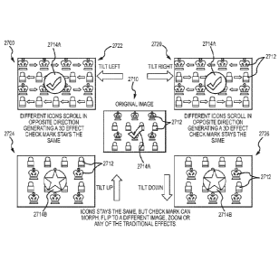
[0073] Figures 11 and 12 illustrate two exemplary assemblies useful as anti-
counterfeiting devices
for currency or the like that are configured with a lens array and printed
image to provide differing
motion effects. Particularly, the sets 1100 and 1200 of diagrams in Figures 11
and 12 are useful for
showing how the round, hexagon, parallelogram, or square-based lens arrays
when combined with a
printed image with the dual-axis interlacing/combination described herein can
be effectively used to
provide selected motion effects. Due in part to the complex interlacing
process that provides pixel
mapping, the assemblies shown in Figures 11 and 12 are particularly useful as
anti-counterfeiting
devices (which may be applied to currency, product labels, and other
objects/items) as they are very
difficult to reproduce.
[0074] In the diagrams 1100 of Figure 11, a plan or orthogonal view 1110 of a
lens/image assembly
according to the present description is shown. The viewer is able to observe
or view an original
image with rows of two differing icons with the icons all being stationary or
non-moving. In
diagram or view 1120, the assembly is tilted or angled to the right (e.g.,
through or to an angle of 15
to 45 degrees or the like), and the interlacing of the matrix of frames (a set
of different points of
view (POVs) of the original image shown in view 1110 such as a matrix similar
to that shown in
Figure 7) is configured to cause the rows of different icons to move in
opposite directions. For
example, rows with padlock icons move to the right while company logos/icons
move to the left. In
19
CA 2923132 2017-10-17
CA 02923132 2016-03-03
WO 2015/034551 PCT/US2014/018920
contrast, in diagram or view 1122, the assembly is tilted or angled to the
left (e.g., through or to an
angle of 15 to 45 degrees or the like), and the interlacing of the matrix of
frames is configured to
cause the rows of different icons again to move in opposite directions. For
example, rows of
padlock icons may move to the left while the company logos/icons concurrently
move to the right.
In other words, the printed image is adapted to provide animation of the
original image when the
lens/printed image (or ink layer) is viewed from differing angles or points of
view (e.g., the
assembly or anti-counterfeiting device shown in view 1110 is pivoted about a
first or vertical axis).
[0075] Significantly, the assembly of an array of lenses with an ink layer
providing a dual-axis
interlaced image provides animation or motion in more than one direction. In
diagram or view
1124, the assembly is tilted or angled upward (e.g., through or to an angle of
15 to 45 degrees or the
like by pivoting about a second or horizontal axis of the assembly), and the
interlacing of the matrix
of frames (a set of different points of view (POVs) of the original image
shown in view 1110 such
as a matrix similar to that shown in Figure 7) is configured to cause the rows
of different icons to
move in a single direction (e.g., all move upward). In contrast, in diagram or
view 1126, the
assembly is tilted or angled downward (e.g., through or to an angle of 15 to
45 degrees or the like
about a horizontal axis of the assembly), and the interlacing of the matrix of
frames is configured to
cause the rows of different icons again to move in a single direction (e.g.,
all move downward). In
other words, the printed image is adapted to provide animation of the original
image when the
lens/printed image (or ink layer) is viewed from differing angles or points of
view (e.g., the
assembly or anti-counterfeiting device shown in view 1110 is pivoted about a
second or horizontal
axis).
[0076] In the diagrams or views 1200 of Figure 12, a plan or orthogonal view
1210 of a lens/image
assembly according to the present description is shown. The viewer is able to
observe or view an
original image with rows of two differing icons with the icons all being
stationary or non-moving.
In diagram or view 1220, the assembly is tilted or angled to the right (e.g.,
through or to an angle of
15 to 45 degrees or the like), and the interlacing of the matrix of frames (a
set of different points of
view (POVs) of the original image shown in view 1210 such as a matrix similar
to that shown in
Figure 7) is configured to cause the rows of different icons to move in a
single direction (rather than
in opposite directions as shown in 1120 of Figure 11). For example, rows with
padlock icons and
company logos/icons all move downward when the assembly (or anti-
counterfeiting device) is tilted
to the right. In contrast, in diagram or view 1222, the assembly is tilted or
angled to the left (e.g.,
through or to an angle of 15 to 45 degrees or the like), and the interlacing
of the matrix of frames is
configured to cause the rows of different icons again to move in a single
direction such as upward.
In the embodiment shown in Figure 12, the printed image is adapted to provide
animation of the
original image when the lens/printed image (or ink layer) is viewed from
differing angles or points
of view (e.g., the assembly or anti-counterfeiting device shown in view 1210
is pivoted about a first
or vertical axis). The animation as shown can be in a direction that is
transverse relative to the
pivoting directions.
[0075] Significantly, as discussed relative to Figure 11, the assembly of an
array of lenses with an
ink layer providing a dual-axis interlaced image provides animation or motion
in more than one
direction. In diagram or view 1224, the assembly is tilted or angled upward
(e.g., through or to an
angle of 15 to 45 degrees or the like by pivoting about a second or horizontal
axis of the assembly),
and the interlacing of the matrix of frames (a set of different points of view
(POVs) of the original
image shown in view 1210 such as a matrix similar to that shown in Figure 7)
is configured to cause
the rows of different icons to move in single direction but one that differs
from that found during
left or right tilting (e.g., all move or scroll to the right). In contrast, in
diagram or view 1226, the
assembly is tilted or angled downward (e.g., through or to an angle of 15 to
45 degrees or the like
about a horizontal axis of the assembly), and the interlacing of the matrix of
frames is configured to
cause the rows of different icons again to move or scroll in a single
direction (e.g., all move to the
left). In other words, the printed image is adapted to provide animation of
the original image when
the lens/printed image (or ink layer) is viewed from differing angles or
points of view (e.g., the
assembly or anti-counterfeiting device shown in view 1210 is pivoted about a
second or horizontal
axis).
[0076] Figure 13 illustrates a set of images or views 1300 of another
lens/printed image (ink layer)
assembly as may be seen by a viewer in differing positions or with the
assembly tilted or moved to
change the viewing angle for the viewer. The assembly may take the form of an
array of round,
hexagonal, parallelogram, or square-based micro lenses overlying a dual-axis
interlaced image
(printed onto the back, planar surface of the lens array or on a substrate
(e.g., paper currency, a
plastic card, a paper or plastic label, or the like) upon which the lens array
is later attached). The
21
CA 2923132 2017-10-17
CA 02923132 2016-03-03
WO 2015/034551 PCT/US2014/018920
plastic card, a paper or plastic label, or the like) upon which the lens array
is later attached). The
interlaced image is printed using a print file that is generated as discussed
above to combine a
matrix of frames (e.g., sets of 2 to 4 or more frames of a single image/scene
taken at differing POVs
relative to the horizontal and vertical axes) to provide pixel mapping.
[0079] In Figure 13, image or view 1310 shows a straight-on or orthogonal view
of the assembly or
anti-counterfeiting device 1300, and the image is a company logo in this
example. Image or view
1320 is visible to a viewer when the assembly is tilted up as shown with arrow
1321 (the planar
assembly is rotated upward about a horizontal or first axis of the assembly).
As shown, view/image
1320 shows additional information relative to the original image seen in view
1310 such as the
bottom side of the logo or object that has been the subject of the interlaced
image file. Another
image or view 1322 is visible by a viewer when the assembly is rotated or
tilted to the right as
shown with arrow 1323 (the planar assembly is rotated or tilted about a
vertical axis (e.g., a second
axis orthogonal or at least transverse to the first axis of the assembly)).
More information or
imagery is visible in the view 1322 such as the left side of the logo or other
object that was the
subject of the interlaced image file.
[0080] Further, another view or image 1324 is viewed when the assembly is
rotated or tilted 1325
downward (rotated about a horizontal or first axis), and, in this view 1324,
information not seen in
the other views is presented such as the top side of the logo or other imaged
object. View or image
1326 provides more information or portions of the target object such as the
right side of the
logo/target object, and the view 1326 is visible when the assembly is rotated
or tilted 1327 about a
vertical or the second axis of the assembly.
[0081] Figure 14 illustrates a set of views/images 1400 of another embodiment
or implementation
of a lens/printed image assembly (or anti-counterfeiting device) 1410. As
shown in view/displayed
imagery 1412, the assembly 1410 (a micro lens array as described herein
positioned over a dual-axis
interlacing of a matrix of frames corresponding to differing images of a
scene/object from differing
points of view) is seen from a point of view that is normal or orthogonal to a
front surface 1411 of
the assembly 1410. In some embodiments, the front surface 1411 is provided by
the outer surfaces
of an array of round, hexagonal, parallelogram, or square-based lenses. As
shown, the viewer can
see a background that contains a static wallpaper pattern (of icons and
padlocks). The icons/image
22
CA 02923132 2016-03-03
WO 2015/034551 PCT/US2014/018920
components may appear very deep in the plane of the film and may be visible in
each viewing angle
(e.g., are visible in views 1414, 1416 when the assembly 1410 is tilted right
or left). The overlay
pattern is in the plane of the film but is not visible (or only slightly
visible) when viewed straight on
as shown in view 1412 (but can be seen in views 1414 and 1416).
[0082] View 1416 is useful for showing a display provided by the interlaced
image of assembly
1410 when the assembly is tilted at a shallow angle (tilted or rotated
slightly to the left about a
vertical axis). When tilted at a shallow angle (e.g., up to about 15 degrees
or the like), the overlay
pattern is only visible in black on the area of the film or front surface 1411
of the assembly 1410
that is closest to the viewer. The printed image may be configured such that
tilting slightly (e.g.,
less than about 15 degrees) in any side direction (up, down, left, or right or
rotating of the assembly
1410 about either the vertical or horizontal axis) causes the overlay pattern
to gradually become
visible (appears black in this example). The pattern is an "overlay" that
appears to be on the top of
or covering over the icons or wallpaper pattern in the plane of the film (or
outer surface 1411 of the
assembly 1410).
[0083] At shallow angles, the overlay is first visible on the portion of the
film or assembly 1410
closest to the viewer. When the assembly 1410 is tilted further away from the
viewer (such as to
angles of about 30 to 45 degrees or more), more and more of the overlay
pattern gradually becomes
visible until the entire overlay pattern is visible when the assembly 1410 is
viewed via surface 1411
at a predefined more extreme angle (e.g., an angle of 45 to 60 degrees or more
relative to the normal
view 1412). This can be seen in extreme angle view 1414 of Figure 14 where the
assembly 1410 is
rotated about a vertical axis (e.g., to the right) more than about 60 degrees.
In view 1414, the
overlay pattern is fully visible over the wallpaper pattern with the icons
(logos and padlocks in this
example) over the entire surface 1411 of the assembly/film 1410.
[0084] Figure 15 illustrates an assembly 1510 of another embodiment of the
present description.
The assembly 1510 may be configured for use as an anti-counterfeiting device
or label with a
body/substrate, an ink layer providing a printed image with dual-axis
interlacing of a matrix of
differing POV frames as discussed herein, and an array of round, hexagonal,
parallelogram, or
square-based lenses for viewing the printed image. For example, the assembly
1510 may be a label
(e.g., a 2-inch by 1 inch or other sized label) that may be printed down a web
on 1.125-inch centers
23
CA 02923132 2016-03-03
WO 2015/034551 PCT/US2014/018920
or the like during its manufacture. The assembly 1510 includes a front or
upper surface 1512 (e.g.,
a thin lens array formed of transparent or at least translucent plastic or
similar material) through
which an interlaced image (image built using the pixel mapping taught herein)
may be viewed as
shown. The printed image may include a void or blank space as shown with white
(or other-
colored) box 1513, which may be used for printing (e.g., flcxo) barcodcs
and/or human-readable
text, which may be added offline or in later processing (e.g., via thermal
transfer printing).
[0085] The assembly/label 1510 has a printed image that has been specifically
designed to provide
a number of images and effects to make it more difficult to reproduce and to
allow a viewer to
readily verify its authenticity. For example, the printed image presents a
gray background 1516
(e.g., that may be subsurface printed (e.g., flexo)) upon which icons or
symbols 1514, 1517 (colored
and/or black) may be printed or layered. The symbol 1517 may take the form of
a boundary (e.g. a
circle) in which a second symbol or text is provided such as text (e.g., "OK")
that should be
completely inside the boundary to show the label 1510 is not a counterfeit or
is authentic.
[0086] The printed interlaced image may also include devices/components for
further allowing a
viewer to check the authenticity of the label 1510. For example, a magnifying
glass image 1520
may be incorporated into printing plates used to fabricate the assembly/label
1510 and appear on the
plane of the film or surface 1512. One or more of the icons/symbols 1523, 1525
may be provided
within the image 1520 such as under the glass of the magnifying glass of image
1520. Then, the
printed image may be configured such that, when a viewer looks through the
glass area of image
1520, the icons 1523 appear black and the icons 1525 appear blue, which may be
a different color
than these icons 1514, 1517 appear in the rest of the label 1510 (e.g.,
reverse the coloring of these
icons when viewed under the glass image 1520). Further the icons 1523 and 1525
under the
magnifying glass image 1520 may appear to be somewhat larger in size than the
corresponding
wallpaper/background versions of these icons 1514, 1517.
[0087] The wallpaper icons 1530 may be designed to move in opposite (or the
same) directions
when the assembly 1510 is tilted about a first axis (e.g., the assembly/label
is rotated/tilted to the left
or right) while moving in the same (or opposite) directions when the assembly
1510 is tilted about a
second axis (e.g., the assembly/label is rotated/tilted upward or downward).
In contrast in some
embodiments of the label 1510, the corresponding icons/symbols 1523, 1525
under the magnifying
24
CA 02923132 2016-03-03
WO 2015/034551 PCT/US2014/018920
glass image 1520 may be designed to move differently than those icons 1530
that are not under the
glass. For example, the icons 1523, 1525 may move together in a single
direction under the glass
image 1520 while the icons 1530 move, as shown with arrows 1531, in opposite
directions when the
assembly 1510 is rotated/tilted about a particular axis.
[0088] The printed image under the lens array of assembly 1510 may include a
further element
(e.g., a boxed/bordered display) 1540 to enhance security (or limit
counterfeiting efforts further).
The element 1540 may include a border 1549, which may be formed of a pattern
that is difficult to
reproduce such as a 0.15-mm (or other size) microtext border containing one or
more intentional
misspellings (e.g., the border appears solid to the naked eye of a viewer but
misspelled words are
evident under a microscope). In the normal view as shown in Figure 15, a first
image 1541 is
displayed but, as shown in the exploded view, a second image 1542 is displayed
in the element
1540 when the assembly 1510 is rotated 1543 about a first axis (e.g., rotated
right or left about a
vertical axis of assembly 1510). To further enhance security, a third image
1544 may be displayed
in the element 1540 when the assembly 1510 is rotated 1545 in another
direction (e.g., rotated up or
down about a horizontal axis of assembly 1510).
[0089] Figure 16 illustrates a system 1600 adapted for use in fabricating an
assembly such as an
anti-counterfeiting device as described herein. The system 1600 includes an
imaging workstation
1610 with a processor 1612 for executing code or software programs to perform
particular
functions. The workstation 1610 may take the form of nearly any computer
device with the
processor 1612 acting to manage operation of input and output devices 1614
such as devices for
allowing an operator of the station 1610 to view and input data useful by the
mapping and imaging
module 1620 to create a print file 1648 communicated as shown at 1675 to a
print controller 1680.
The CPU 1612 also manages memory 1630 accessible by the mapping and imaging
module 1620.
[0090] The mapping and imaging module 1620 performs the functions useful in
performing the
functions and processes described herein such as for generating frame sets
1640 from an original
image 1632, creating a frame matrix 1646 from these image sets 1640, and
producing a
bidirectional bit map or print file 1648 (i.e., print file using pixel
mapping) from the frame matrix
1646. For example, the memory 1630 may be used to store an original image 1632
that may
CA 02923132 2016-03-03
WO 2015/034551 PCT/US2014/018920
include a background 1634 as well as one or more icons/symbols 1636 that may
be provided as
wallpaper (e.g., these elements may be layered over the background 1634).
[0091] The module 1620 may act to generate a number of sets of frames 1640
from the original
image 1632, and each of the sets 1640 may include 2 to 10 or more frames from
differing points of
view of the original image (e.g., see the sets of frames shown in Figure 7
that provide differing POV
frames along two axes (X and Y axis frames/images of a base or original image
1632)). The
module 1620 may generate a frame matrix 1646 as discussed above to properly
map the pixels to
provide proper X and Y axis interlacing with or without a motion effect. From
the matrix 1648, a
bidirectional pixel map or print file 1648 is generated by combining the rows
and columns of the
matrix 1646 with proper sequencing (with all 3D and/or motion information in
both directions such
as with squares with the data from the matrix 1646 rather than stripes).
[0092] The mapping and imaging module 1620 may generate the print file 1648
based on a variety
of imaging/mapping parameters 1650. For example, the lens array design
information 1652
including whether the lenses are round, hexagonal, parallelogram, or square,
the optical pitch 1654,
and the LPI 1656 values may be taken as input by the module 1620 to create the
print file 1648.
Further, the device output resolution 1670 may be used by the module 1620 to
create the print file
1648 such as to set the number of frames in the sets 1640 or the like. The
parameters 1650 may also
include motion parameters 1660 to define how to animate the original image
with tilting/rotating of
an assembly such as by setting the direction of movement of the icons/symbols
and how fast
movement occurs (how much rotation needed to achieve a particular motion
effect and so on). The
parameters 1650 may also include color parameters 1666 such as whether or not
icons/symbols
change colors with rotation of an assembly with an image printed from file
1648 and what such
colors should be in the displayed image.
[0093] Once a print file 1648 is created, the imaging workstation 1610 may
communicate (in a
wired or wireless manner such as over a digital communication network) this
file 1648 to a print
controller 1680 (e.g., another computer or computing device). The print
controller 1682 may use
this print file 1648 to fabricate a printing or embossing plate 1682, which
can then be used to
emboss a surface such as the planar/back side of a lens array with fabrication
device 1684. This
embossed surface can then be filled with one or more coatings/layers of ink to
form a printed image
26
CA 02923132 2016-03-03
WO 2015/034551 PCT/US2014/018920
in a lens array/printed image assembly (e.g., an anti-counterfeiting device).
The controller 1680
may also use the print file 1648 to provide a digital file 1670 to a color,
digital printer 1674 for
printing of the dual-axis interlaced image on a surface such as the planar
back side of a lens array or
on a side of a piece of paper currency or a product label over which a lens
array is later applied to
provide an anti-counterfeiting device on the currency/label.
[0094] At this point, it may be useful to describe techniques for performing
pixel adjustment that
may be performed (at least in part) by a software module/program such as the
mapping and imaging
module 1620 of Figure 16. Figure 17 illustrates with a flow diagram a pixel
adjustment method
1700 according to the present description. The method 1700 includes at 1710
performing a print
test (e.g., with components 1680 to 1684 of Figure 16) to determine the
optical pitch, in the X axis
and also in the Y axis, of a lens array, which as discussed above, may vary
from design. At 1720, a
target visual pitch is selected for a desired or input viewing distance
(again, in the X and Y axes).
For example, as shown at 1730, the method 1700 may involve setting the target
pitch at 416.88 for
the X axis and 384.47 for the Y axis.
[0095] The method 1700 continues at 1740 with interlacing the X and Y axes in
the pixel map.
This typically involves mapping at the nearest device output for the desired
target pitch (e.g., 400
output is near to the pitches set at step 1730). In step 1750, the method 1700
includes calculating
the difference between the device output and the target optical pitch. In this
example, the difference
in the X axis is +4.22 percent (i.e., Target Pitch of 416.88 divided by the
device output of 400) and
the difference in the Y axis is -3.9 percent (e.g., Target Pitch of 384.47
divided by the device output
of 400).
[0096] At step 1760, the mapping and imaging module/software program acts to
remove pixels
based on the differences determined in step 1750. In this example, the module
may remove 4.22
percent of the pixels by specifically targeting low information areas in the X
axis. The module may
also act to add 3.9 percent pixels in the Y axis. Step 1770 of method 1700
further explains this
process with the module acting to identify pixels with less information for
removal (e.g., evenly in
the X axis in this example) while the adding of pixels may be performed by
blending pixels such as
nearby (e.g., blending pixels are added in the Y axis). At 1780, plates are
output based on the print
file modified to provide pixel adjustment. In this working example, the plates
for printing may be
27
CA 02923132 2016-03-03
WO 2015/034551 PCT/US2014/018920
output at 4800 pixels in the X axis and 4800 pixels in the Y axis. At 1790, it
is noted that the
process 1700 retains integrity of the displayed image without blur, e.g., due
to re-resolution pristine
pixels.
[0097] Figure 18 is useful for further explaining the process of providing
dual-axis interlacing for a
lens array of the present description. A small lens array or lenslet 1810 is
shown in a plan or top
view that includes four lenses 1812, 1814, 1816, and 1818 (with a more typical
array having many
more lenses). As shown at 1815, the lenses 1812, 1814, 1816, and 1818 are
round-based lenses in
this non-limiting example. Underneath the lens array 1810, a dual-axis printed
image (or ink layer
with a printed image) can be provided with each of the boxes 1813 in the
figure being used to
represent a pixel. Further, each of these "pixels" 1813 can be considered to
be a lens focus point.
[0098] The printed image provided in pixels 1813 when combined with lens array
1810 provides a
display device that can be used to provide full 3D imagery as well as multi-
directional motion. For
example, each lens 1812, 1814, 1816, 1818 may be used to display a looping
image. To this end,
the diagonal sets of pixels 1830 shown with shading may be used to provide a
45 degree tilt loop
sweep while the horizontal and vertical sets of pixels 1820 shown with "stars"
may be used to
provide a side-to-side and up-and-down image loop.
[0099] With this in mind, graph 1850 is useful for illustrating how an
arrangement of 7 pixels by 7
pixels provided under each lens 1812, 1814, 1816, and 1818 may be printed with
dual-axis
combined/interlaced images to provide these effects. In this example, four
frames in the X axis are
combined with four frames in the Y axis (e.g., "X=3" refers to a particular
frame in the set of four
frames along the X axis). A mapping and imaging module (such as module 1620)
may be used to
select the proper frames to generate such a matrix and/or print map, and a
print file can be generated
from this mapping for use in printing the dual-axis interlaced images in each
pixel as shown in
graph 1850 so as to provide the visual effects described with pixels 1820,
1830.
[00100] Figures 19-21 are plots 1900, 2000, and 2100 showing ray tracing
for assemblies of
the present description, e.g., for a lens array combined with a dual-axis
interlaced image.
Particularly, Figure 19 illustrates a plot 1900 of a tracing of rays 1920
using an assembly 1910 (e.g.,
an anti-counterfeiting device) configured as described herein. As shown, the
assembly 1910
28
CA 02923132 2016-03-03
WO 2015/034551 PCT/US2014/018920
includes a lens array 1912 of round-based lenses 1914 overlying an ink
layer/printed image 1916
including a number of interlaces 1918 (7 images are interlaced using dual-axis
interlacing).
[00101] The plot 1900 shows rays 1920 traced from idealized lenticular
interlaced stripes
1918 in printed image/ink layer 1916. The order of the interlaces was modified
so that to the viewer
the image is properly interlaced. In this example, the radius of each lens
1914 was 1.23 mils, the
lenses 1914 were provided at 408 LPI, the lenses 1914 were 3 mils thick, and
the index of refraction
was assumed to be 1.49. For clarity, only zero width interlaces were
represented with 7 interlaces
1918 per sets of two lenses 1914. Tracings were made over a range of +30
degrees to -30 degrees
with 5 degree steps showing the near lenticule region.
[00102] The plot 2000 is a filled-in ray trace showing a larger overall
view of the plot 1900 of
Figure 19. The interlaces for plot 2000 were taken to be 2 mils wide with 7
interlaces provided per
set of two lenses. Five steps per interlace were traced, the range was +30
degrees to -30 degrees
using 1 degree steps. The sequence of the interlaces was 6, 4, 2, 3, 7, 5, and
1. The plot 2100 is a
trace done with a normal sequence of the interlaces (e.g., 1, 2, 3, 4, 5, 6,
and 7) for a lens of radius
1.23 mils, lenses provided at 408 LPI, a lens thickness of 3 mils, and an
index of refraction of 1.49.
The lens width was taken at 2 mils, and there were 7 interlaces provided for
each set of two lenses.
Five steps were traced across each lens again with a range of +30 degrees to -
30 degrees with 1
degree steps. In summary, the plots 1900, 2000, and 2100 show coding that is
done by having
multiple interlaces per multiple lenticules and the change in distribution to
the viewer by changing
the interlace sequence.
[00103] In analyzing use of the lens arrays of the present invention with
dual-axis interlaced
print images, it is useful to generate ray tracings and spot diagrams to check
a planned array/image
design. In this regard, Figure 22 is a plot 2200 of an off-axis ray tracing
while Figure 23 is a
corresponding spot diagram 2300 that may be generated to analyze a planned
array/image design.
Further, Figures 24 and 25 are two additional spot plots or diagrams 2400 and
2500 for a round-
based lens (or spherical lens), while Figure 26 is a plot 2600 of a ray
tracing for the lens associated
with the plots of Figures 24 and 25. The radius of the lens for these latter
three figures was 5 units
and the focal plane was about 10 units (e.g., the units may be any unit such
as mils).
29
CA 02923132 2016-03-03
WO 2015/034551 PCT/US2014/018920
[00104] Although the invention has been described and illustrated with a
certain degree of
particularity, it is understood that the present disclosure has been made only
by way of example, and
that numerous changes in the combination and arrangement of parts can be
resorted to by those
skilled in the art without departing from the spirit and scope of the
invention, as hereinafter claimed.
[00105] The description teaches a display assembly (e.g., an anti-
counterfeiting device) that
includes an array of round or square lenses combined with an ink layer with a
printed image/pattern.
The lens arrays are made up of nested round, hexagonal, parallelogram, or
square lenses arranged as
shown in the attached figures. The printed image/pattern provided in the ink
layer (or layers) are
aligned with the lens arrays (e.g., with the X and Y axes of the printed
image), and the printed
image/pattern is made up of vertically and horizontally mapped pixels (e.g.,
printed using a print file
defining dual-axis interlacing (or interlacing in two axis) of frames of a
matrix as discussed herein).
The pixels may be of any type and often are adapted to match the output device
with the viewer's
optical pitch in two axes. The lens arrays may be provided at 200 or more LPI
in both directions so
as to provide 4000 lenses or more per square inch. The focal lengths of the
lenses may vary, but
some arrays have been implemented that have focal lengths of less than about
10/1000 inches for
round and for square-based lenses.
[00106] The printing of the dual-axis interlaced image for use with a lens
array may be
performed using one or more colors using the pixel mapping provided in a
generated print file. In
some cases, diffractive techniques are used to create color with the
separation of wave lengths,
purposefully or accidentally, within the interlaced image in a round-based
lens array. Particularly,
the printing step involves printing of an X and Y pixel-imaged file or pixel
map so as to produce a
printing plate or a digital image, either of which may be used to provide an
ink layer with a printed
image/pattern that is useful in combination with the round and square-based
lenses as nested in an
array as described herein (e.g., printing on the back or planar surface of the
lens material to provide
the X and Y axis pixel mapped images). In other cases, an embossing plate is
produced for use to
emboss the back of the lens material (lens array). Then, the embossed back
surface is filled with ink
or metalized for use in holography in combination with a round or square-based
lens array. In some
cases, though, printing may also occur on the front or contoured surface of
the lens array. For
example, the printing may involve printing features, colors, or images
directly on top of the lenses
(i.e., the non-planar side of the lens array) in combination with printing on
the back or planar side of
the lenses using interlaced images.
[00107] A number of unique visual or display effects can be achieved with
the printed image
viewed through one of the lens arrays of the present description. For example,
image mapping of
the X and Y axes may be performed so that a wallpapered array of repeating
icons (e.g., the
company logos and padlocks of the exemplary figures) scroll or move across the
substrate in
opposite directions to each other when the substrate (or assembly or anti-
counterfeiting device) is
tilted left and right (rotated about a vertical or first axis) and in the same
direction when the
substrate is tilted up and down (rotated about a horizontal or second axis
transverse to the first axis).
This effect may be called "Continuum Movement in Opposite Directions."
[00108] In other cases, the image mapping is performed so that a
wallpapered array of
repeating icons moves or scrolls up and down across the surface of the
assembly/anti-counterfeiting
device when the assembly/device is tilted left and right (icons all move in
the same direction) and
left and right when the assembly/device is tilted up and down (again, all
icons move in the same
direction) (e.g., tilt left causes all icons to scroll or move upward, tilt
right causes all icons to scroll
move down, tilt up causes all icons to scroll right, and tilt down causes all
icons to scroll left). This
effect may be labeled "Continuum Movement in Orthogonal Directions."
[00109] Image mapping of the X axis and Y axis pixels may be performed such
that a
volumetric icon or image like a company logo or a symbol has five viewable
sides (e.g., a top side, a
bottom side, a left side, a right side, and a face or front side). These five
sides are viewable in three
dimensions, with apparent depth and in full parallax, when the assembly/device
is tilted or rotated in
differing directs (orthogonal/normal view, tilt left, tilt right, tilt upward,
and tilt downward or a
positioning therebetween). The face of the 3D logo/symbol/icon may be a
different color than the
sides to create a more noticeable 3D effect, and this effect may be called
"full volume 3D."
[00110] Another effect that can be achieved via the image mapping of the X
axis and the Y
axis described herein is to provide wallpaper with icons with another overlay
pattern. Then, the
overlay pattern may be provided in the print file and resulting printed image
so that it is hidden from
view when the assembly is viewed from certain POVs (such as a normal POV) but
gradually
31
CA 2923132 2017-10-17
CA 02923132 2016-03-03
WO 2015/034551 PCT/US2014/018920
becomes more and more visible (in the plane of the film and wallpaper pattern)
on top of the
icons/symbols/logos of the wallpaper (such as when moved to angles of 30 to 60
degrees or the like
from normal). Further, it is not required that the entire printed image
provide a single effect.
Instead, different zones or portions of the printed image may be used to
provide differing visual
effects (e.g., any of the effects described herein).
[00111]
Several means are available to implement the systems and methods discussed in
this
specification. These
means include, but are not limited to, digital computer systems,
microprocessors, application-specific integrated circuits (ASTC), general
purpose computers,
programmable controllers and field programmable gate arrays (FPGAs), all of
which may be
generically referred to herein as "processors." For example, in one
embodiment, signal processing
may be incorporated by an FPGA or an ASIC, or alternatively by an embedded or
discrete
processor. Therefore, other embodiments include program instructions resident
on computer
readable media which when implemented by such means enable them to implement
various
embodiments. Computer readable media include any form of a non-transient
physical computer
memory device. Examples of such a physical computer memory device include, but
are not limited
to, punch cards, magnetic disks or tapes, optical data storage systems, flash
read only memory
(ROM), non-volatile ROM, programmable ROM (PROM), erasable-programmable ROM (E-
PROM), random access memory (RAM), or any other form of permanent, semi-
permanent, or
temporary memory storage system or device. Program instructions include, but
are not limited to,
computer-executable instructions executed by computer system processors and
hardware
description languages such as Very High Speed Integrated Circuit (VHSIC)
Hardware Description
Language (VHDL).
[00112] While
Figures 11-15 illustrate a number of the effects that can be achieved using
the
pixel mapping techniques described herein in combination with arrays of micro
lenses, it may be
useful at this time to discuss these unique effects in more detail. Pixel
mapping (or dual-axis
interlacing) allows one to generate a print file with a plurality of pixels
each generated with the
specific purpose of allowing activation of an effect about one of two axes. In
other words,
activation in 2 axes requires or is at least enhanced by pixel mapping as
taught herein. The "effects"
that can be achieved (including those shown in Figures 11-15) may be thought
of as the same set of
32
effects achieved in a single axis using lenticular lenses and interlacing of
images in a single
direction. These effects, however, can now be provided one (or two, three, or
more) at a time in
each direction using pixel mapping, and the anti-counterfeiting devices may
use any combination of
these effects (with one provided in each direction in many cases). The effects
include 3D, motion,
flip (change an image into another or modified image), animation, on/off (make
an image appear
and disappear with rotation about an axis or with "activation"), zoom, morph
(like a flip but can
view the transition to the new image), and color shift (change color as part
of the activation).
[00113] As a first example, a lens array and printed image assembly may be
designed and
fabricated to provide 3D in one axis (such as in the X axis) and to provide an
effect activation in the
a second axis transverse (such as orthogonal) to the first axis (such as by
providing activation in the
Y axis). The 3D may be provided in a first axis of the assembly with patterns
or elements in
different layers (such as by having a foreground image over one or more
background images).
Then, activation of additional effects may be provided in the second axis such
as: (a) motion (e.g.,
elements moving or with displacement in the frame; (b) flip (e.g., an image
"A" changing to image
"B" for 2-image flip or more than two images may be used to provide more
flipping); (c) animation
(e.g., a sequence of frames may be used to describe or define animation of
images); (d) on/off (e.g.,
single or multiple elements may be provided in the frames that appear or
disappear depending on
the viewing angle; (e) zoom (e.g., single or Multiple element enlarging or
reducing of size of a
displayed image may be provided that depends upon the viewing angle); (f)
morph (e.g., effect can
be like a flip from image "A" to image "B" but with transition frames included
in between final
images so that it is possible for viewer to see the transformation from image
"A" to image "B"); and
(g) color shift (e.g., single or multiple elements can change color with
activation that may be
triggered by rotation of assembly through multiple viewing angles or POVs).
[00114] With these combinations in mind, Figure 27 illustrates a set of
views 2700 of an
exemplary assembly viewed from differing POVs, with the assembly being useful
as an anti-
counterfeiting device for currency or other objects that are configured with a
lens array and printed
image to provide differing motion effects (dual-axis activation). In the
diagrams or views 2700 of
Figure 27, a plan or orthogonal view 2710 of a lens/image assembly according
to the present
description is shown. The viewer is able to observe or view an original image
with rows of two
33
CA 2923132 2017-10-17
differing icons 2712 with the icons 2712 all being stationary or non-moving.
Further, the original
image includes an overlay image or foreground image 2714A (shown here as a
checkmark) that
appears to be in a different layer than the rows of icons 2712. Hence, the
assembly is adapted to
provide a 3D effect. In the figures, rows of two icons are shown, but it will
be understood that this
was done for ease of explanation only and not as a limitation. With rows of
two icons understood
and how they may be used to provide security with activation in two axes, it
will be understood that
each row may include two or more differing icons (rather than a single icon
per row) and rows of a
third, fourth, or more differing icon may be included in the assembly as
desired to achieve a desired
displayed image.
[00115] In diagram or view 2720, the assembly is tilted or angled to the
right (e.g., through or
to an angle of 15 to 45 degrees or the like), and the interlacing of the
matrix of frames (a set of
different points of view (POVs) of the original image shown in view 2710 such
as a matrix similar
to that shown in Figure 7 is used in pixel mapping) is configured to cause the
rows of different icons
2712 to move in opposite directions. For example, rows with padlock icons
and/or logos 2712
move left and right when the assembly (or anti-counterfeiting device) is
tilted to the right. In
contrast, in diagram or view 2722, the assembly is tilted or angled to the
left (e.g., through or to an
angle of 15 to 45 degrees or the like), and the interlacing of the matrix of
frames is configured to
cause the rows of different icons again to move in differing directions from
each other and in the
opposite direction as in view 2720 (icons 2712 that moved to the right now
move to the left and vice
versa).
[00116] In the embodiment shown in Figure 27, the printed image is adapted
to provide
animation of the original image when the lens/printed image (or ink layer) is
viewed from differing
angles or points of view (e.g., the assembly or anti-counterfeiting device
shown in view 2710 is
pivoted about a first or vertical axis). The animation as shown can be in a
direction that is parallel
to the pivoting directions. However, the print file is configured such that
some images such as
foreground or other layer image 2714A, remains in the same relative location,
and this movement of
background or other layer icons (as these moving icons 2712 could be
foreground images and
symbol/icon 2714A could be provided in the background layer) enhances or even
provides the 3D
effect of the assembly.
34
CA 2923132 2017-10-17
CA 02923132 2016-03-03
WO 2015/034551 PCT/US2014/018920
[00117] Further, the 3D effect can be combined with additional effects when
the assembly is
activated in another or the second of two orthogonal axes. As shown, the
assembly of an array of
lenses with an ink layer presenting a dual-axis interlaced image provides
animation and a 3D effect
in one direction or when activated along one axis and flipping (or morphing)
in a second direction
or when activated along a second axis. In diagram or view 2724, the assembly
is tilted or angled
upward (e.g., through or to an angle of 15 to 45 degrees or the like by
pivoting about a second or
horizontal axis of the assembly), and the interlacing of the matrix of frames
(a set of different points
of view (POVs) of the original image shown in view 2710 such as a matrix
similar to that shown in
Figure 7) is configured to cause the icons 2712 to stay the same or remain
unchanged while the
symbollicon 2714A in the other layer (foreground image) flips (or morphs) to a
different image
2714B (here, a check mark flips into a star).
[00118] Similarly, in diagram or view 2726, the assembly is tilted or
angled downward (e.g.,
through or to an angle of 15 to 45 degrees or the like about a horizontal axis
of the assembly), and
the interlacing of the matrix of frames is configured to cause the rows of
icons 2712 to remain
stationary while the foreground or other layer symbeicon 2714A flips (or
morphs) into a different
image 2714B (here the same image as when the assembly is tilted upward). In
other words, the
printed image is adapted to provide flipping of an image when the assembly is
rotated about a
second axis (such as about the horizontal or X-axis). Flipping is shown in
Figure 27 for the effect
provided when activated in the second direction but the effect may also be
morphing, on/off,
motion, animation, zoom, or color shift.
[00119] To further illustrate the many possible combinations, Figure 28
illustrates a set of
views 2800 of an exemplary assembly viewed from differing POVs, with the
assembly being useful
as an anti-counterfeiting device for currency or other objects that are
configured with a lens array
and printed image to provide differing motion effects (dual-axis activation).
In the diagrams or
views 2800 of Figure 28, a plan or orthogonal view 2810 of a lens/image
assembly according to the
present description is shown, and the assembly is configured to provide 3D
from all viewpoints
(e.g., floating and/or depth) along with the same or different image elements
having a Y-axis or X-
axis activation (to have motion, to flip, to morph, or another of the effects
achievable with
interlacing of image frames). The viewer is able to observe or view an
original image with rows of
two differing icons 2812 with the icons 2812 all being stationary or non-
moving. Further, the
original image includes first and second overlay images or foreground images
2814A and 2816A
(shown here as the word "OK" and a check-nark symbol) that appear to be in a
different layer than
the rows of icons 2812. Hence, the assembly is adapted to provide a 3D effect.
[00120] In diagram or view 2820, the assembly is tilted or angled up (e.g.,
through or to an
angle of 15 to 45 degrees or the like), and the interlacing of the matrix of
frames (a set of different
points of view (POVs) of the original image shown in view 2810 such as a
matrix similar to that
shown in Figure 7 is used in pixel mapping) is configured to cause the rows of
different icons 2812
to move in a single direction (e.g., all icons move downward or opposite the
activation direction).
With this movement of the assembly (tilt up), the foreground images 2814A and
2816A remain
unchanged (e.g., no flip at this point). The movement of the icons 2812
underneath (or over the top
in some embodiments) the symbols 2814A, 2816A heightens the 3D effect achieved
with the
assembly.
[00121] In contrast, in diagram or view 2822, the assembly is tilted or
angled downward (e.g.,
through or to an angle of 15 to 45 degrees or the like), and the interlacing
of the matrix of frames is
configured to cause the rows of different icons again to move in a single
direction (but this time
upward or opposite the activation direction). Concurrently, though, a flip
effect is also activated
with the foreground symbol/icon 2814A flipping to an image as shown at 2814B
(e.g., from the
word "OK" to the word "Yes"), while the other symbol/icon 2816A remains
unchanged in this
example. From the view 2822 to the view 2820, flipping will again occur as the
symbol 2814B will
change back or flip back to image 2814A (e.g., flipping effect is activated
with rotation about the
horizontal or X-axis of the assembly concurrently with the movement effect for
icons 2812 (in a
single direction in this non-limiting example)).
[00122] Further, the 3D effect can be combined with additional flip effects
when the assembly
is activated in another or the second of two orthogonal axes. As shown, the
assembly of an array of
lenses with an ink layer presenting a dual-axis interlaced image provides
animation and a 3D effect
in one direction or when activated along one axis and flipping (or morphing)
in a second direction
or when activated along a second axis. In diagram or view 2824, the assembly
is tilted or angled to
the left (e.g., through or to an angle of 15 to 45 degrees or the like by
pivoting about a second or
36
CA 2923132 2017-10-17
horizontal axis of the assembly), and the interlacing of the matrix of frames
(a set of different points
of view (POVs) of the original image shown in view 2810 such as a matrix
similar to that shown in
Figure 7) is configured to cause the icons 2812 to be placed in motion with
the icons 2812 moving
in the same direction (again opposite the activation direction and this is
orthogonal to the earlier
movement directions of views 2820 and 2822). Concurrently, the symbol/icon
2814A (or 2814B)
in the other layer (foreground image) remains unchanged while the symbol/icon
2816A does not flip
but is activated to have a morph effect in that it changes as shown at 2816B
to be spun to a new
position (e.g., the checkmark in this example has a new orientation, which may
also be considered
an animation effect).
[00123] Similarly, in diagram or view 2826, the assembly is tilted or
angled to the right (e.g.,
through or to an angle of 15 to 45 degrees or the like about a horizontal axis
of the assembly), and
the interlacing of the matrix of frames is configured to cause the rows of
icons 2812 to again have a
motion effect (move in single direction such as opposite the activation
direction) while the
foreground or other layer symbol/icon 2816A again is morphed (or animated) to
spin into image
2816B. In other words, the printed image is adapted to provide 3D with
foreground images that can
be flipped, morphed, or animated with activation and such activation effects
can be independent
from each other and from the background images. Further, the printed image
provides concurrent
motion effects with background images, which are shown to be activated to move
together in a
single direction that is opposite the activation direction. With the icons
2812 moving in the
directions shown, the result is a depth effect (e.g., 3D) where the icons 2812
appear to be pushed
back from the foreground symbols/icons 2814A-2816B. This effect can also be
combined with
some layers being pushed toward the front or outward toward the viewer.
[00124] To still further illustrate the many possible combinations, Figure
29 illustrates a set of
views 2900 of an exemplary assembly viewed from differing POVs, with the
assembly being useful
as an anti-counterfeiting device for currency or other objects that are
configured with a lens array
and printed image to provide differing motion effects (dual-axis activation).
In the diagrams or
views 2900 of Figure 29, a plan or orthogonal view 2910 of a lens/image
assembly according to the
present description is shown, and the assembly is configured to provide
activation in a first axis
(such as the X-axis) that achieves orthogonal movement of the image elements
combined with
37
CA 2923132 2017-10-17
activation in a second axis (such as the Y-axis) of the same or different
image elements. The viewer
is able to observe or view an original image with rows of two differing icons
2912 with the icons
2912 all being stationary or non-moving. Further, the original image includes
first and second
overlay images or foreground images 2914A and 2916A (shown here as the word
"OK" and a
checkmark symbol) that appear to be in a different layer than the rows of
icons 2912. Hence, the
assembly is adapted to provide a 3D effect.
[00125] In diagram or view 2920, the assembly is tilted or angled to the
right (e.g., through or
to an angle of 15 to 45 degrees or the like), and the interlacing of the
matrix of frames (a set of
different points of view (POVs) of the original image shown in view 2910 such
as a matrix similar
to that shown in Figure 7 is used in pixel mapping) is configured to cause the
rows of different icons
2912 to move in a single direction (e.g., all icons move downward or
orthogonal to the activation
direction). With this movement of the assembly (tilt right), the foreground
images 2914A and
2916A remain unchanged (e.g., no flip at this point). The movement of the
icons 2912 underneath
(or over the top in some embodiments) the symbols 2914A, 2916A heightens the
3D effect achieved
with the assembly.
[00126] In contrast, in diagram or view 2922, the assembly is tilted or
angled to the left (e.g.,
through or to an angle of 15 to 45 degrees or the like), and the interlacing
of the matrix of frames is
configured to cause the rows of different icons again to move in a single
direction (but this time
upward (which is opposite the movement shown in view 2920) and orthogonal to
the activation
direction). Concurrently, though, a flip effect is also activated with the
foreground symbol/icon
2914A flipping to an image as shown at 2914B (e.g., from the word "OK" to the
word "Yes"),
while the other symbol/icon 2916A remains unchanged in this example. From the
view 2922 to the
view 2920, flipping will again occur as the symbol 2914B will change back or
flip back to image
2914A (e.g., flipping effect is activated with rotation about the vertical or
Y-axis of the assembly
concurrently with the movement effect for icons 2912 (in a single direction in
this non-limiting
example)).
[00127] Further, the 3D effect can be combined with additional flip effects
when the assembly
is activated in another or the second of two orthogonal axes. As shown, the
assembly of an array of
lenses with an ink layer presenting a dual-axis interlaced image provides
animation and a 3D effect
38
CA 2923132 2017-10-17
CA 02923132 2016-03-03
WO 2015/034551 PCT/US2014/018920
in one direction or when activated along one axis and flipping (or morphing)
in a second direction
or when activated along a second axis. In diagram or view 2924, the assembly
is tilted or angled
upward (e.g., through or to an angle of 15 to 45 degrees or the like by
pivoting about a second or
horizontal axis of the assembly), and the interlacing of the matrix of frames
(a set of different points
of view (POVs) of the original image shown in view 2910 such as a matrix
similar to that shown in
Figure 7) is configured to cause the icons 2912 to be placed in motion with
the icons 2912 moving
in the same direction (again orthogonal to the activation direction which may
be to the right as
shown in this example) . Concurrently, the symbol/icon 2914A (or 2914B) in the
other layer
(foreground image) remains unchanged while the symbol/icon 2916A does not flip
but is activated
to have a morph effect in that it changes as shown at 2916B to be spun to a
new position (e.g., the
checkmark in this example has a new orientation, which may also be considered
an animation
effect).
[00128] Similarly, in diagram or view 2926, the assembly is tilted or
angled downward (e.g.,
through or to an angle of 15 to 45 degrees or the like about a horizontal axis
of the assembly), and
the interlacing of the matrix of frames is configured to cause the rows of
icons 2912 to again have a
motion effect (move in single direction such as to the left and so as to move
orthogonal to the
activation direction (or the vertical or Y-axis of the assembly) while the
foreground or other layer
symbol/icon 2916A again is morphed (or animated) to spin into image 2916B.
[00129] Figure 30 illustrates another assembly 3010 useful as an anti-
counterfeiting device
that may be used on or with currency or the like. The assembly 3010 may be
formed with a top or
outer surface 3102, which may be provided with a lens array. The assembly 3010
may also include
an ink layer(s) providing a printed image printed using a print file with
pixel mapping as described
herein to provide dual-axis activation (or activation of image effects such as
3D, motion, or the like)
in two axes. Particularly, the printed image of assembly 3010 is adapted to
allow viewing of a
background image made up of a plurality of smaller symbols/icons 3014 (such as
the checkmarks
shown in Figure 30). The printed image of assembly 3010 also is adapted to
allow viewing
(through lens array/front surface layer 3012) a foreground image made up of
one or more
symbols/icons (which are typically larger than the background image elements
3014).
39
CA 02923132 2016-03-03
WO 2015/034551 PCT/US2014/018920
[00130] In some implementations of the assembly 3010, the printed image is
pixel mapped to
the lens array in a manner that full 3D is provided in all directions by
providing the image elements
3014 and 3018 in 2 or more layers. As shown in Figure 30, the background image
or pattern
provided by symbols/icons 3014 is pushed back away from a viewer to appear to
be behind the
foreground image made up of symbols/icons 3018. The elements 3018 may be
provided as larger
elements, and they may be caused to appear to float in different levels
relative to image elements
3014 from all view points. This may be achieved in part by causing the images
3018 to remain
stationary during dual-axis activation (rotating of the assembly 3010 about
the X and Y-axes) while
the background images 3018 are caused to move (apply a motion effect to the
image elements
3014).
[00131] Other assemblies may be created that include a print image formed
using pixel
mapping chosen to provide patterns or images that are activated in a first
axis (e.g., the X-axis) with
any of the effects listed or described herein. Further, the print image may be
configured to provide a
combination of the same image elements (e.g., an icon or symbol) or different
image elements being
activated in a second axis (e.g., the Y-axis) with any one of the effects
listed or described (the same
or differing effects). For example, the effects may include, but are not
limited to: (a) a 3D layered
effect (e.g., image elements displayed so as to appear in different layers
with each layer being a flat
image); (b) a 3D real effect (e.g., provide a picture or 3D element generated
by 3D software or the
like); (c) a motion effect (e.g., image elements that are moving or with
displacement in the frame);
(d) a flip effect (e.g., an image "A" changing to an image "B" for 2-image
flip or more than two
images may be used in a flip effect); (e) animation (e.g., sequence of frames
that describes or
defines animation for one or more image elements); (f) an on/off effect (e.g.,
single or multiple
image elements may be caused to appear or disappear depending on the viewing
angle for the
assembly); and (g) a zoom effect (e.g., single or multiple image elements may
be enlarged or
reduced in size depending on the viewing angle of the printed image through
the array of round,
hexagonal, parallelogram, or square-based micro lenses).
[00132] Figures 3A-4B provide examples of items formed using round-based
and square-
based lenses to form lens arrays. Further, these lens arrays were specifically
patterned or arranged
to not use offset or nested rows and columns of lenses (e.g., the lenses in
adjacent rows and columns
CA 02923132 2016-03-03
WO 2015/034551 PCT/US2014/018920
were aligned rather than offset). The use of pixel mapping as taught herein by
the inventors has
allowed anti-counterfeiting devices with lens array/printed image assemblies
to be fabricated
effectively with the use of lens arrays with offset/nested lenses and also
with lens arrays that are
configured to include hexagon lenses or hexagonal-based lenses. Hence, Figures
31 and 32 provide
specific working examples of such implementations.
[00133] In an embodiment shown in Figure 31, an item 3100 (such as a piece
of paper
currency, a label for a product, or the like) is provided with an anti-
counterfeiting element or device
in the form of a lens array (array of hexagonal-based lenses) 3110 covering or
provided on top of a
layer of ink 3120 providing a printed image. As shown, the item 3100 includes
a substrate or body
3105 such as a sheet of paper or plastic (e.g., paper to be used as currency
or paper/plastic to be used
for a product label). On a surface of the substrate/body 3105, an image is
printed via a layer of ink
3120, and a lens array 3110 is provided on an exposed surface of the ink layer
3120 (e.g., the ink
layer 3120 and its pattern/image may be printed onto the substrate surface or
onto the back surface
of the lens array 3110).
[00134] As shown, the lens array 3110 is made up of a plurality of lenses
3114 that each have
a hexagonal base abutting the surface of the ink layer 3120 and have a dome-
shaped cross section
and/or one two or more facets/sides. The hexagonal-based lenses or round
lenses 3114 are arranged
in a number of columns 3112 that are parallel as shown by parallel vertical or
Y-axes 3113 (axes
passing through the center of the lenses 3114 in columns 3112) in Figure 31.
Further, the lenses
3114 are arranged such that pairs of lenses 3114 in adjacent ones of the
columns 3112 are in contact
or proximate at least at the bases. Still further, the columns 3112 are
vertically offset such that pairs
of adjacent lenses 3114 in a particular column 3112 are spaced apart. Then,
the array 3110 is
configured to have parallel rows of lenses 3114, each abutting their
neighboring lenses in such rows
(or nearly contacting each other at the bases), as can be seen by parallel
horizontal or X-axes 3115
passing through centers of lenses 3114 in the array 3110, and the rows are
shown to be abutting
each other and to also be offset (e.g., to have a horizontal offset as well as
vertical offset). In this
way, the lenses 3114 may be tightly nested in the pattern shown in Figure 31
(note, the array 3110
may be rotated for use such as rotation of 90 degrees such that the "columns"
become "rows" and
vice versa).
41
CA 02923132 2016-03-03
WO 2015/034551 PCT/US2014/018920
[00135] In an embodiment shown in Figure 32, an item 3200 (such as a piece
of paper
currency, a label for a product, or the like) is provided with an anti-
counterfeiting element or device
in the form of a lens array (array of round-based lenses) 3210 covering or
provided on top of a layer
of ink 3220 providing a printed image. As shown, the item 3200 includes a
substrate or body 3205
such as a sheet of paper or plastic (e.g., paper to be used as currency or
paper/plastic to be used for a
product label). On a surface of the substrate/body 3205, an image is printed
via a layer of ink 3220,
and a lens array 3110 is provided on an exposed surface of the ink layer 3220
(e.g., the ink layer
3220 and its pattern/image may be printed onto the substrate surface or onto
the back surface of the
lens array 3210).
[00136] As shown, the lens array 3210 is made up of a plurality of lenses
3214 that each has a
round or circular base abutting the surface of the ink layer 3220 and have a
dome-shaped cross
section and/or one two or more facets/sides. The round lenses 3214 are
arranged in a number of
columns 3212 that are parallel as shown by parallel vertical or Y-axes 3213
(axes passing through
the center of the lenses 3214 in columns 3212) in Figure 32. Further, the
lenses 3214 are arranged
such that pairs of lenses 3214 in adjacent ones of the columns 3212 are in
contact or proximate at
least at the bases. Still further, the columns 3212 are vertically offset such
that pairs of adjacent
lenses 3214 in a particular column 3212 are spaced apart. Then, the array 3210
is configured to
have parallel rows of lenses 3214, each abutting their neighboring lenses in
such rows (or nearly
contacting each other at the bases), as can be seen by parallel horizontal or
X-axes 3215 passing
through centers of lenses 3214 in the array 3210, and the rows are shown to be
abutting each other
and to also be offset (e.g., to have a horizontal offset as well as vertical
offset). In this way, the
lenses 3214 may be tightly nested in the pattern shown in Figure 32 (note, the
array 3210 may be
rotated for use such as rotation of 90 degrees such that the "columns" become
"rows" and vice
versa).
[00137] As discussed in the initial portion of this document, moire
patterns have been used in
conjunction with round and hexagonal lens arrays for many years. Typically the
printed images are
small fine images relative to the size of the lenses. Some of the images are
printed in a frequency
slightly more frequent or less than the one to one dimension of the lenses in
two axes and some are
printed slightly differently relative to each other. The result is a moire
pattern that shows the
42
CA 02923132 2016-03-03
WO 2015/034551 PCT/US2014/018920
illusion of depth of field with the lenses to the viewer or shows motion of
the items to the viewer.
Typically, these lens arrays combined with printing of an image are used in
the anti-counterfeiting
market for labels and currency. The thickness of the lenses is under 5/1000-
inch and down to about
.5/1000-inch (i.e., 125 microns to about 12 microns). The frequency of these
lenses is about 400 X
400 to over 1000 X 1000 per inch.
[00138] While useful to a point, the effects one can achieve with moire
patterns are limited.
For example, one cannot take a photograph and display 3D with a moire pattern.
Typically, the
moire patterns are used in the security industry in very fine lenses with
focal lengths of about 20 to
75 microns and frequencies of over 500 lenses per inch in one axis (or more
than 250,000 per
square inch). The printed images underlying the lenses are typically at least
12,000 DPI and may go
to over 25,000 DPI, with the micro-lens arrays being closely nested (e.g., as
shown in Figures 1 and
2). In other cases, these lenses can be quite course at 30 lenses in a linear
inch with focal lengths of
more than 0.125 inches or even 0.25 inches and only about 900 lenses per
square inch.
[00139] One significant problem with the use of moire images is that they
can be relatively
easily reverse engineered. It is easy to see the patterns underlying the lens
with a cheap microscope
and determine the frequency of the images and patterns. In addition, the
lenses can be cast and re-
molded making counterfeiting possible. The relative difficulty in reverse
engineering comes in
printing the images, but this is also getting easier to achieve due to high-
resolution lasers and setters.
[00140] Typically, the micro-lenses are printed using an emboss-and-fill
technology. This
generally limits the printing to one color due to the fact that the process
tends to be self-
contaminating after one color, as well as the fact that the process is
difficult to control from a
relative color-to-color pitch in the emboss and fill printing process. Some
have implemented a
motion technology that uses emboss-and-fill, high-resolution printing that is
one color due to the
fact the web or sheet is pre-embossed, flood coated with an ink and wiped
clean (absent the
embossed areas) and a blade leaves ink residue and contaminants making
additional colors
challenging. Another problem relative to the general web stretch and movement
is that the small
optical pitch differences needed for magnifying moires are difficult to
achieve due to differences in
run tensions between colors.
43
CA 02923132 2016-03-03
WO 2015/034551 PCT/US2014/018920
[00141] Hence, the inventors determined that there was a need for anti
counterfeiting devices
that are much more difficult, if not impossible to duplicate. Preferably, it
was determined that these
devices should also be designed to have the "wow" factor for overt display of
images floating above
the focal plane and below the focal plane.
[00142] Printed lens arrays can be difficult to print in either sheet or
web form (especially web
form) in offset, gravure, flexo or any other method. Some of the problems lie
with the devices that
make plates or "plate-setters" as well as the physical ability to print a very
small dot or image. This
fact when combined with the registration inaccuracies in equipment, film
stretch, and other
variables make it impossible or difficult to print very high resolution images
needed in micro-lens
arrays in 4-color process or with any real accuracy. These facts limit what
can be done in printed
micro lenses.
[00143] General print accuracies limitations found in press manuals can be
found as follows
(color to color registration): (1) Best Sheetfed Press (Heidelberg or Komori)-
8 microns; (2) Best
Currency Press (Sheet only-KBA Notsys)-4 to 6 microns; (3) Best Web (Gravure
or Flexo)-150
plus microns; and (4) Best Central Impression Web -50 microns. Further,
physics dictates that the
thinner the substrate or lens array used (needed for security and anti
counterfeiting) the finer or
smaller the lens array is for the target thickness and focal length
relationship. The basic formula is
the following: (A) Chord Width=C; (B) Radius of Lens= R; (C) Focal Length=F
(or lens thickness);
and (D) LPI= Lens frequency or number of lenses in a lineal inch. Then, basic
lens physics
indicates: R>.5(C). Further, F=1.5(C) (as an approximation).
[00144] For example, a currency thread can be printed in multiple colors in
patterns and plain
colors at about 25 microns. The minimum realistic LPI in both directions to
make this possible is
about 1200 LPI, which requires a minimum of 5 pixels for decent 3D or
animation. Therefore, 5 X
1200 = 6000 DPI in both directions. However, much better quality dictates 10
images and about
12,000 DPI. Non-registering patterns and so forth can be printed showing
motion and 3D in
multiple colors. However, the registration requirements for printing color to
color, 4¨color process,
or registering colors together at this level is impossible or at least
extremely difficult with past
technology. The lens width or chord width (C) in this case is about 21
microns. Since one pixel is
needed for each frame and 5 frames are needed for each lens, the print
requirement for even a single
44
CA 02923132 2016-03-03
WO 2015/034551 PCT/US2014/018920
color is difficult. Looking at the discussion above, the best web presses
register color to color at
about 50 microns. The registration requirement for 4-color process or other
tight multiple color
processes with a chord width of about 21 microns (5 frames, each at 4.2
microns) is about 2-3
microns. Unfortunately, this has proven difficult to impossible to achieve
with current technology.
[00145] Producing non-holographic imagery (printed imagery) in registration
in even one axis
is impossible with current technology with more than one color. Obviously,
photographs in motion
or 3D are impossible under lens arrays regardless of the print technology. The
practical limitation
with today's technology in web is really non-existent (the thickness of the
material would
necessarily be over 15/1000" and about 100 LPI to possibly register color to
color, and would not
practically wind in a web). Therefore, printed and registered color would be
limited to sheet fed
offset technology (not practical for banknotes or labels for security).
[00146] A novel way to address this problem is needed for the technology to
advance beyond
traditional printing. In the microwave part of the spectrum, where there are
few losses, patterned
and perforated metal films or films coated with metal on the sub-wavelength
scale achieve spectral
selectivity by balancing the transmission and reflective characteristics of
the surface. For optical
frequencies, where joule losses are important, the planned structure of a
metal film (without
perforation) or a violation of continuity is sufficient to provide or achieve
substantial modification
of reflectivity. By engineering the geometry of the structure imposed or
embossed onto the surface,
one can dramatically change the "perceived" color of the metal without the use
of chemicals, thin-
film coating, or diffraction effects.
[00147] This novel selective frequency effect underlies plasmonic joule
losses in continuous
elements of the patterns ("intaglio" and "bas relief') in the metamaterials to
distinguish both the
raised and indented portions of the structures, and it is specific to the
optical part of the spectrum.
Such a technology has the advantage of maintaining the integrity of the metal
structures on the
surfaces and is scalable for high production techniques and fabrication.
[00148] The highest possible resolution for printed color images is
determined by the
diffraction limit of visible light. To hit the "limit," individual color
elements, which are or may be
considered "pixels," with a pitch of 250 nm (e.g., a pitch of less than 10,000
nanometers (or 10
CA 02923132 2016-03-03
WO 2015/034551 PCT/US2014/018920
microns) such as in the range of 200 to 300 nanometers or less than about 300
nm) are required or
desired for making the effective print resolution (often given as dots per
inch (DPI)) at about
100,000 DPI (or a range of 10,000 to 125,000 DPI or at least about 10,000 DPI
in some cases while
others may use at least 75,000 DPI). Color information can be encoded in the
dimensional
parameters of the metal nano structures so that tuning their plasmonic
resonance determines the
color of the individual pixels. This type of color mapping produces images
with sharp color
differences as well as fine tonal variations. The method can be used for large
volume color printing
without ink via nanoimprint lithography.
[00149] This technology can be used to reproduce the entire spectrum of
visible colors from
distinct colors to RGB blends and CMYK process colors for the reproduction of
photographs or
other images. It is important to note that, unlike diffraction imagery, the
resulting colors from the
manipulation of the balance of reflected and transmitted waves are largely
insensitive to viewing
angle. Therefore, since combining these nanostructures tuned to produce color
pixels simulating up
to 100,000 DPI with lens arrays as described herein using both moire and
interlaced images results
in incoming light (due to the lens focus) of different entry angles, the
resulting color back to the
viewer is not distorted or changed as it is with diffraction patterns.
Interlaced images with lenses
that focus on individual pixels or groups of pixels remain as designed when
presented or reflected
back to the viewer and color remains unchanged. The resulting color is largely
unaffected due to
the incoming angle.
[00150] For the above reasons, combining lens arrays as described herein
with this
"plasmonic resonance" technology makes the ideal, or at least a very useful,
combination for thin
film 4-color processes and for providing combined and registered color for
lens arrays for uses in
security, branding, and other applications. For the first time, one can use
the dramatic color effects
that can be produced in a single step intaglio/bas relief metamaterial. It can
be applied equally to a
bulk and thin film surface and can be implemented into a single step process.
The mapping of the
pixels can be done post interlacing or mapping of the 3D or animated image.
The images can be
interlaced first and then converted at the pixel level to the proper
conversion method (continuous
intaglio or bas relief) to simulate the desired color.
46
[00151] An example of the astounding depth of features and animation that
can occur is
illustrated by the conventional counterpart (traditional print combined with
these lenses) that would
be at 75 microns. Even in the proofing environment (images impossible to
register and print in
production), a maximum of 6 images for a 400 LPI lens (bi-directional round or
square based lens)
by 6 images could be achieved at about 2400 DPI. Conversely, the plasmonic
resonance system
described above allows a very sharp focusing lens to be designed that will
provide the pixels at 75
microns. Rather than a 6 by 6 frame pattern (36 images in a lens), a 250 image
by 250 image
pattern could be achieved at 100,000 DPI with 62,500 views or image frames in
process colors,
straight colors (PMS equivalents), or RGB colors. Hence, plasmonic resonance
facilitates larger
frame patterns than the 6 by 6 patterns such as 7 by 7 frame patterns (49
image frames) up to 250 by
250 frame patterns (62,500 image frames).
[00152] The lens array can then be cast, extruded, or laminated to the nano-
bas relief or
embossed film that contains the imagery or the nano-bas relief structures. The
optical pitch of the
lens can be designed and fabricated to match the exact resonance of the color
pixels generated by
the nano-bas relief structures or the inverse. The optical pitch can be scaled
to match the lens array
exactly by the systematic removal of pixel sets (formed by sets of nano
structures) or addition of
nanostructures formulated in blending (non-interfering) colors or pixels so
that the exact resolution
of the device writing the file is matched without interpolation down to about
250 nanometers.
[001531 Using plasmonic resonance or continuous metal frequency for
creating imagery using
interlaced files allows the finite adjustment of a file down to the combined
nanopost combination
creating color resonance at the 250 rim level. This pixel "replacement"
represents a final pixel, and
therefore, the adjustment to match the optical pitch (imagery) to the
microlens goes down to about
250 mn. This is ideal for creating a precise match between the micro lens and
the image itself, as it
allows a finite adjustment without using ancillary programs that cause
averaging and distortion in
the file.
[00154] With regard to general interlacing for all lens arrays using
continuous metal
frequency technology, images may be created in a normal way using photographs,
Adobe's
Photoshop Illustrator, or any number of programs. The color file is then
separated into color zones
via color separation software that may be in RGB or CMYK for the images. This
is done at a very
47
CA 2923132 2017-10-17
CA 02923132 2016-03-03
WO 2015/034551 PCT/US2014/018920
high resolution so that the pixels may be broken down to make color builds at
up to about 100,000
DPI, with about 250 nm per pixel. The shapes of the nanoposts are then formed
to match the
appropriate color given the plasmonic resonance associated with that color
when matching the wave
length to the electron. This can be done in the color separation software.
[00155] The individual color selections for those pixels are then
translated into the appropriate
physical shapes of the micro-structures (nanoposts) to create the proper color
to the viewer.
However, before the final selection of the shapes, the files are interlaced
for 3D and/or animation
down to the possible level of one pixel per frame or 250 nm depending upon the
size of the file and
or micro lens. The files are then interlaced to match the lenses, whether
round, square, hexagonal,
linear, parallelogram-type, or aspheric lenses are used in the lens array. The
pixels are then
translated (after interlacing) with software that identifies the colors and
the pixels and provides the
necessary data to create the nanoposts or micro-embossing file containing X, Y
and Z coordinates.
[00156] With regard to lens application and general manufacturing, after
the files are created
with the interlaced images and converted into embossing files, a plastic
substrate may be embossed
first and then metalized appropriately, with the exact metamaterials used
varying from application
to application. The materials may be individually conductive materials or
combinations of
conductive materials such as gold, aluminum, silver and so forth. These
materials may be vapor
coated with layers of 2 to 50 or more nanometers of material. Conversely, the
film itself may be
pre-coated with the metamaterials and post-embossed with the nano-structures.
[00157] The lenses (again, any of the previously mentioned types/shapes may
be used) may
be applied after the process of metallization and embossing or even before.
The lens array is
formed on or as part of the film and the metallization occurs, and this is
followed by embossing on
the planar side of the lens. However, when the lens is applied afterward, the
adhesive and or
stamping process and associated hot melt adhesive and the index of refraction
should be taken into
account to calculate the appropriate focal lengths.
[00158] In summary, the lens or array of micro lenses: (1) may be applied
after the
production of the substrate, embossing, and metallization; (2) may be embossed
with the lens array
first extruded or cast first and then embossed with the nano-interlaced images
(then metalized with
48
CA 02923132 2016-03-03
WO 2015/034551 PCT/US2014/018920
the metamaterials); and (3) may be made, metalized, and then embossed on the
backside (planar
side).
49
CA 02923132 2016-03-03
WO 2015/034551 PCT/US2014/018920
PROGRAM LISTING OR SUBROUTINE FOR RAY TRACING FOR DUAL-AXIS
INTERLACING AND ROUND OR SQUARE-BASED LENS ARRAYS
Sub Intersect_Nearest_Surface(xs, ys, zs, elx, ely, elz, xi, yi, zi, enx, eny,
enz, gnfound,
snfound, surftypefound, success)
'finds surface nearest to starting point of ray.
'inputs
'xs,ys,zs starting point of ray
' c 1 x,c 1 y,c 1 z direction cosines of ray
'xi,yi,zi intersection point of ray
'returns
'gnfound,snfound group number, surface number found
'surfacetypefound of nearest surface.
'sucess (if found)
Dim intplaneflag, IntSphere5flag, IntCylinderFlag, IntEllipsoidFlag As Boolean
Dim icolor, k As Integer
Dim surftypetemp As String
Dim intsphere3planeflag As Boolean
Dim gn, sn, gntemp, sntemp As Integer
Dim distance As Double
Dim xitemp, yitemp, zitemp As Double
CA 02923132 2016-03-03
WO 2015/034551 PCT/US2014/018920
Dim enxtemp, enytemp, enztemp As Double
Dim xp, yp, zp As Double
Dim XP1, YP1, ZP1 As Double
'Dim enx, eny, enz As Double
Dim enxx, enyy, enzz As Double
Dim enxplane, enyplane, enzplane As Double
Dim xc, yc, zc, rr As Double
Dim x0, yO, z0 As Double
Dim Tx, ry, rz As Double
'Dim rxl, ryl, rzl, rx2, ry2, rz2 As Double
'Dim xil, yil, zil, xi2, yi2, zi2 As Double
Dim gx, gy, gz As Double
Dim a, b, c, xvertex As Double
Dim riml, toll, sl As Double
toll = 0.0001
'go through all the surfaces that have been defined, intersect each one and
find the surface
nearest to the starting point of the
'incident ray.
success = False
distance = 10 A 10
51
CA 02923132 2016-03-03
WO 2015/034551 PCT/US2014/018920
For gn = GroupStart To GroupEnd Step GroupStep
For sn = SurfaceStart(gn) To SurfaceEnd(gn) Step SurfaceStep
'plane surface
If SurfaceType(gn, sn) = 1 Then
xp = x(gn, sn)
yp = y(gn, sn)
zp = z(g-n, sn)
enx = Xdir(gn, sn)
eny = Ydir(gn, sn)
cnz = Zdir(gn, sn)
Call intplanc2(xs, ys, zs, clx, cly, clz, xp, yp, zp, cnx, cny, cnz, xi, yi,
zi,
intplaneflag)
If intplaneflag = True Then
sl = Scir((xi - xs) A 2 + (yi - ys) A 2 + (zi - zs) A 2)
If s 1 < distance And sl > toll Then
distance = s 1
xitemp = xi
yitemp = yi
zitemp = zi
enxtemp = enx
52
CA 02923132 2016-03-03
WO 2015/034551
PCT/US2014/018920
enytemp = eny
enztemp = enz
surftypetemp = "Plane"
gntemp = gn
sntemp = sn
End If
End If 'intplane=true
End If
'spherical surface
If SurfaceType(gn, sn) = 2 Then
xc = x(gn, sn)
ye = y(gn, sn)
zc = z(gn, sn)
rr = r(gn, sn)
XP1 = XPlane(gn, sn)
YP1 = YPlane(gn, sn)
ZP1 = ZPlane(gn, sn)
enxplane = ENXP(gn, sn)
enyplane = ENYP(gn, sn)
53
CA 02923132 2016-03-03
WO 2015/034551 PCT/US2014/018920
enzplane = ENZP(gn, sn)
Call IntSphere5(xs, ys, zs, elx, ely, elz, xc, ye, zc, rr, Tx, ry, rz, xi, yi,
zi,
IntSphere5flag)
'Call IntSphere3_Plane_Divide(xs, ys, zs, elx, ely, elz, xc, ye, zc, rr, XP1,
YP1, ZP1,
enxplane, enyplane, enzplane, Tx, ry, rz, xi, yi, zi, intsphere3planeflag)
'Call IntSphere2(xs, ys, zs, elx, ely, elz, xc, ye, zc, rr, Tx, ry, rz, xi,
yi, zi,
intsphereflag)
If IntSphere5flag = True Then
'If IntSphere5flag = True Then '= 1 Or intsphereflag = 2 Then
sl = Sqr((xi - xs) A 2 + (yi - ys) A 2 + (zi - zs) A 2)
s 1 < distance And sl > tol I Then
distance = sl
xitemp = xi
yitemp = yi
zitemp = zi
enxtemp = rx '999999?999?99999
enytemp = ry
enztemp = rz
surftypetemp = "Sphere"
gntemp = gn
54
CA 02923132 2016-03-03
WO 2015/034551
PCT/US2014/018920
sntemp = sn
End If
'If intsphereflag = 2 Then
sl = Sqr((xi2 - xs) A 2 + (yi2 - ys) A 2 + (zi2 - zs) A 2)
' If s1 < distance And sl > toll Then
distance = sl
' xitemp = xi2
yitemp = yi2
' zitemp = zi2
enxtemp = rx2 ,?799799?799?7997
enytemp = ry2
enztemp = rz2
surftypetemp = "Sphere"
gntemp = gn
sntemp = sn
' End If
'End If 'intsphereflag=2
'End If 'intsphere=1 or 2
End If 'intsphere <>0
CA 02923132 2016-03-03
WO 2015/034551 PCT/US2014/018920
End If 'spherical surface
'cylinder surface
If SurfaceType(gn, sn) = 3 Then
x0 = x(gn, sn)
y0 = y(gn, sn)
z0 = z(gn, sn)
gx = Xdir(gn, sn)
gy = Ydir(gn, sn)
gz = Zdir(gn, sn)
rr = r(g-n, sn)
Call intcylindcr(xs, ys, zs, clx, cly, clz, x0, yO, zO, gx, gy, gz, rr, xi,
yi, zi, cnx, cny,
enz, IntCylinderFlag)
If IntCylinderFlag = True Then
sl = Scir((xi - xs) A 2 + (yi - ys) A 2 + (zi - zs) A 2)
If s 1 < distance And sl > toll Then
distance = s 1
xitemp = xi
yitemp = yi
zitemp = zi
enxtemp = enx
56
CA 02923132 2016-03-03
WO 2015/034551 PCT/US2014/018920
enytemp = eny
enztemp = enz
surftypetemp = "Cylinder"
gntemp = gn
sntemp = sn
End If
End If
End If
'Aperture
If SurfaceType(gn, sn) = 4 Then
xp = x(gn, sn)
yp = y(gn, sn)
zp = z(gn, sn)
enx = Xdir(gn, sn)
eny = Ydir(gn, sn)
enz = Zdir(gn, sn)
Call intplane(xs, ys, zs, elx, ely, elz, xp, yp, zp, enx, eny, enz, xi, yi,
zi, intplaneflag)
If intplaneflag = True Then
s I = Sqr((xi - xs) A 2 + (yi - ys) A 2 + (zi - zs) A 2)
57
CA 02923132 2016-03-03
WO 2015/034551
PCT/US2014/018920
If s 1 < distance And sl > toll Then
distance = sl
xitemp = xi
yitemp = yi
zitemp = zi
enxtemp = enx
enytemp = eny
enztemp = enz
surftypetemp = "Aperture"
gntemp = gn
sntemp = sn
End If
End If
End If
'Ellipsoid
If SurfaceType(gn, sn) = 5 Then
a = ax(gn, sn)
b = by(gn, sn)
c = cz(gn, sn)
58
CA 02923132 2016-03-03
WO 2015/034551 PCT/US2014/018920
xvertex = x(gn, sn)
riml = RimLocation(gn, sn)
toll = 0.000001 '.00001 seems to give consistant results
Call IntEllipsoid(a, b, c, xvertex, riml, xs, ys, zs, elx, ely, elz, xi, yi,
zi, enx, eny,
enz, IntEllipsoidFlag)
If IntEllipsoidFlag = True Then
sl = Sqr((xi - xs) A 2 + (yi - ys) A 2 + (zi - zs) A 2)
If sl < distance And sl > toll Then
distance = sl
xitemp = xi
yitemp = yi
zitemp = zi
enxtemp = enx
enytemp = eny
enztemp = enz
surftypetemp = "Ellipsoid"
gntemp = gn
sntemp = sn
End If
End If
59
CA 02923132 2016-03-03
WO 2015/034551
PCT/US2014/018920
End If
'Spline
If SurfaceType(gn, sn) = 6 Then
MsgBox ("Trace main does not support spline")
End If
Next sn
Next gn
'Target plane
xp = XTarget
yp = 0#
zp = 0#
enx = 1#
eny = 0#
enz = 0#
Call intplane(xs, ys, zs, elx, ely, elz, xp, yp, zp, enx, eny, enz, xi, yi,
zi, intplaneflag)
If intplaneflag = True Then
sl = Scir((xi - xs) A 2 + (yi - ys) A 2 + (zi - zs) A 2)
If s 1 < distance And s 1 > toll Then
CA 02923132 2016-03-03
WO 2015/034551
PCT/US2014/018920
distance = sl
xitemp = xi
yitemp = yi
zitemp = zi
enxtemp = enx
enytemp = eny
enztemp = enz
gntemp = 0
sntemp = 0
surftypetemp = "Target"
End If
End If
'plot boundaries
'right side
xp = BoundaryRight
yp = 0#
zp = 0#
enx = 1#
61
CA 02923132 2016-03-03
WO 2015/034551
PCT/US2014/018920
eny = 0#
enz = 0#
Call intplane(xs, ys, zs, elx, ely, elz, xp, yp, zp, enx, eny, enz, xi, yi,
zi, intplaneflag)
If intplaneflag = True Then
sl = Sqr((xi - xs) A 2 + (yi - ys) A 2 + (zi - zs) A 2)
If s 1 < distance And s 1 > toll Then
distance = sl
xitemp = xi
yitemp = yi
zitemp = zi
enxtemp = enx
enytemp = eny
enztemp = enz
gntemp = 0
sntemp = 0
surftypetemp = "Boundary"
End If
End If
'left side
62
CA 02923132 2016-03-03
WO 2015/034551
PCT/US2014/018920
xp = BoundaryLeft
yp = 0#
zp = 0#
enx = -1#
eny = 0#
enz = 0#
Call intplane(xs, ys, zs, elx, ely, elz, xp, yp, zp, enx, eny, enz, xi, yi,
zi, intplaneflag)
If intplaneflag = True Then
sl = Sqr((xi - xs) A 2 + (yi - ys) A 2 + (zi - zs) A 2)
If s 1 < distance And s 1 > toll Then
distance = sl
xitemp = xi
yitemp = yi
zitemp = zi
enxtemp = enx
enytemp = eny
enz temp = enz
gntemp = 0
sntemp = 0
63
CA 02923132 2016-03-03
WO 2015/034551
PCT/US2014/018920
surftypetemp = "Boundary"
End If
End If
'top side
xp = 0#
yp = BoundaryTop
zp = 0#
enx = 0#
cny = 1#
cnz = 0#
Call intplane(xs, ys, zs, elx, ely, elz, xp, yp, zp, enx, eny, enz, xi, yi,
zi, intplaneflag)
If intplaneflag = True Then
sl = Sqr((xi - xs) A 2 + (yi - ys) A 2 + (zi - zs) A 2)
Tf s 1 < distance And s 1 > tol 1 Then
distance = sl
xitemp = xi
yitemp = yi
zitemp = zi
64
CA 02923132 2016-03-03
WO 2015/034551
PCT/US2014/018920
enxtemp = enx
enytemp = eny
enztemp = enz
gntemp =0
sntemp = 0
surftypetemp = "Boundary"
End If
End If
'bottom side
xp = 0#
yp = BoundaryBottom
zp = 0#
enx = 0#
eny = -1#
enz = 0#
Call intplane(xs, ys, zs, elx, ely, elz, xp, yp, zp, enx, eny, enz, xi, yi,
zi, intplaneflag)
If intplaneflag = True Then
CA 02923132 2016-03-03
WO 2015/034551
PCT/US2014/018920
sl = Sqr((xi - xs) A 2 + (yi - ys) A 2 + (zi - zs) A 2)
If s1 < distance And sl > toll Then
distance = sl
xitemp = xi
yitemp = yi
zitemp = zi
enxtemp = enx
enytemp = eny
enztemp = enz
gntemp = 0
sntemp = 0
surftypetemp = "Boundary"
End If
End If
'front side
xp = 0#
yp = 0#
zp = 10 A 6
66
CA 02923132 2016-03-03
WO 2015/034551
PCT/US2014/018920
enx = 0#
eny = 0#
enz = -1#
Call intplane(xs, ys, zs, elx, ely, elz, xp, yp, zp, enx, eny, enz, xi, yi,
zi, intplaneflag)
If intplaneflag = True Then
sl = Sqr((xi - xs) A 2 + (yi - ys) A 2 + (zi - zs) A 2)
If s 1 < distance And s 1 > toll Then
distance = sl
xitemp = xi
yitemp = yi
zitemp = zi
enxtemp = enx
enytemp = eny
enztemp = enz
gntemp = 0
sntemp = 0
surftypetemp = "Boundary"
End If
End If
67
CA 02923132 2016-03-03
WO 2015/034551
PCT/US2014/018920
'back side
xp = 0#
yp = 0#
zp = -10 A 6
enx = 0#
eny = 0#
enz = 1#
Call intplane(xs, ys, zs, elx, ely, elz, xp, yp, zp, enx, eny, enz, xi, yi,
zi, intplaneflag)
If intplaneflag = True Then
sl = Sqr((xi - xs) A 2 + (yi - ys) A 2 + (zi - zs) A 2)
If s 1 < distance And s 1 > toll Then
distance = sl
xitemp = xi
yitemp = yi
zitemp = zi
enxtemp = enx
enytemp = eny
enztemp = enz
gntemp = 0
68
CA 02923132 2016-03-03
WO 2015/034551
PCT/US2014/018920
sntemp = 0
surftypetemp = "Boundary"
End If
End If
'final report
If distance < 10 A 9 Then
success = True
xi = xitemp
yi = yitemp
zi = zitemp
enx = enxtemp
eny = enytemp
enz = enztemp
gnfound = gntemp
snfound = sntemp
surftypefound = surftypetemp
End If
69
CA 02923132 2016-03-03
WO 2015/034551 PCT/US2014/018920
If gnfound = GroupEnd And snfound = SurfaceEnd(gnfound) Then
surftypefound = "Final Surface"
End If
End Sub
**************************************************************************
*******************************************************
Sub IntSphere5(xs, ys, zs, elx, ely, elz, xc, ye, zc, r, Tx, ry, rz, xi, yi,
zi, IntSphere5flag)
'xs,ys,zs is starting point of ray
'elx,ely,elz are direction cosines of ray
'xc,yc,zc is center of circle
'r is radius of sphere
'rx,ry,rz are direction cosines of radius at intersection
'xi,yi,zi is intersection of ray on sphere
'intsphereflag = true if intersection found
Dim sl, s2, s3, xl, x2 As Double
Dim LL, Li, L2 As Double
IntSphere5flag = False
s 1 = 2# * ((xs - xc) * e 1 x + (ys - ye) * e ly + (zs - zc) * e 1 z)
CA 02923132 2016-03-03
WO 2015/034551
PCT/US2014/018920
s3 = s 1 A 2 - 4# * s2
'there is no intersection
If s3 <0 Then
Exit Sub
End If
'there is only one intersection
If s3 = 0# Then
LL -s 1 / 2#
GoTo IntSphere250
End If
'there are two intersections
Li = (-Si + Sqr(s3)) / 2#
L2 = (-sl - Sqr(s3)) / 2#
'check for + L and - L for the side of sphere to choose ( compare where xc and
xi is)
If Li <0# And L2 <0# Then
Exit Sub 'no intersection
71
CA 02923132 2016-03-03
WO 2015/034551
PCT/US2014/018920
End If
If Ll > 0# And L2 > 0# Then
If Ll > L2 Then
1=L1
Else
1=L2
End If
'End If
If Li > 0# Then
xi = xs + Li * clx
yi = ys + L 1 * ely
zi = zs + Li * el z
If r > 0# Then
If xi <= xc Then
LL = Li
End If
End If
72
CA 02923132 2016-03-03
WO 2015/034551
PCT/US2014/018920
If r < 0# Then
If xi >= xc Then
LL = Li
End If
End If
End If
If L2> 0# Then
xi = xs + L2 * elx
yi = ys + L2 * c ly
zi = zs + L2 * c I z
If r > 0# Then
If xi <= xc Then
LL = L2
End If
End If
If r < 0# Then
If xi >= xc Then
LL = L2
73
CA 02923132 2016-03-03
WO 2015/034551
PCT/US2014/018920
End If
End If
End If
IntSphere250:
'Ifl <=0 Then
' Exit Sub
'End If
xi = xs + LL * el x
yi ys + LL * ely
zi = zs + LL * clz
rx = (xi - xc) / r
ry = (yi - yc) / r
rz = (zi - zc) / r
sl =rx^ 2 +ry^2 +rzA2
'MsgBox ("Sum of squares of normal direction cosines "& sl )
IntSphere5flag = True
End Sub
74