Note: Descriptions are shown in the official language in which they were submitted.
1
POWER STORAGE DEVICE, POWER STORAGE CONTROL DEVICE, AND
POWER STORAGE CONTROL METHOD
Technical Field
[0001]
The present disclosure relates to a power storage device, a power storage
control device, and a power storage control method. More specifically, the
present
disclosure relates to a power storage device, a power storage control device,
and a
power storage control method for storing electricity in a cell.
Background Art
[0002]
Technologies of equalizing voltages of a plurality of cells which are
connected in series have been proposed in the related art. Patent Literature
1, for
example, proposes an inter-battery voltage equalization circuit in which a
terminal
voltage of a capacitor is boosted by a voltage of a boosting element in which
electric
charges have accumulated and then the electric charges are transferred to a
secondary
battery.
Citation List
Patent Literature
[0003]
Patent Literature: JP 2013-13291A, published January 17, 2013
Summary of Invention
Technical Problem
[0004]
When a potential difference between a plurality of serially connected cells is
high in a case in which voltages of the cells are to be equalized, an
excessive current
may flow to a cell that will receive energy and thus a burden is imposed
thereon.
[0005]
The present disclosure provides a power storage device, a power storage
control device, and a power storage control method for suppressing a burden
imposed
CA 2923589 2019-08-16
CA 02923589 2016-03-07
2
on a cell when voltages of cells are equalized.
Solution to Problem
[0006]
According to the present disclosure, a power storage device includes: a
plurality of cells which are connected in series; a series resonance circuit
configured
to include a reactor and a capacitor; and a power storage control device
configured to
control a connection state of the cells and the series resonance circuit. The
power
storage control device causes energy to be transferred between equal numbers
of cells
via the series resonance circuit.
After the power storage control device connects first cells including at least
one cell to the series resonance circuit, the power storage control device may
connect
second cells which include cells equal in number to the first cells and have a
lower
total voltage than the first cells to the series resonance circuit.
In this case, the power storage control device may select a plurality of
consecutive cells as the first cells, and select consecutive cells equal in
number to the
first cells as the second cells.
On the other hand, when the first cells are connected to the series resonance
circuit and then the direction of a current flowing in the series resonance
circuit
changes, the power storage control device may disconnect the first cells from
the
series resonance circuit. In this case, when the second cells are connected to
the
series resonance circuit and then the direction of a current flowing in the
series
resonance circuit changes, the power storage control device may disconnect the
second cells from the series resonance circuit. In this case, the power
storage control
device may maintain a state in which all the cells are disconnected from the
series
resonance circuit during a set period after the first and/or second cells are
disconnected from the series resonance circuit, and determine whether or not
transfer
of energy is to be finished based on a voltage of the cells during the set
period.
The series resonance circuit may include a resistance, and the power storage
control device may detect the direction of a current flowing in the series
resonance
circuit based on a potential difference of both ends of the resistance.
The power storage control device may switch connection of the series
resonance circuit and the cells using a resonance frequency of the series
resonance
CA 02923589 2016-03-07
3
circuit.
A resonance frequency of the series resonance circuit may be a frequency
when an imaginary component in a Cole-Cole plot of internal impedances of the
cells
measured using an AC impedance method becomes 0.
The power storage control device may cause a cell having a maximum
voltage to be included in the first cells. In this case, the power storage
control device
may cause a cell having a minimum voltage to be included in the second cells.
The power storage device may further include: a switch configured to
connect or disconnect the cells and the series resonance circuit. The power
storage
control device may control a connection state of the cells and the series
resonance
circuit by controlling an operation of the switch.
The cells may have a discharge characteristic that a change of a voltage is
0.25 V or lower in a series of sections spanning 50% or more of a section of a
charge
ratio of 0% to 100%.
According to the present disclosure, a power storage control device is
configured to control a connection state of a plurality of cells which are
connected in
series and a series resonance circuit which includes a reactor and a
capacitor, and to
cause energy to be transferred between equal numbers of cells via the series
resonance
circuit.
According to the present disclosure, a power storage control method is
carried out by a control device which controls a connection state of a
plurality of cells
which are connected in series and a series resonance circuit which includes a
reactor
and a capacitor to cause energy to be transferred between equal numbers of
cells via
the series resonance circuit.
Advantageous Effects of Invention
[0007]
According to the present disclosure, a burden imposed on a cell when
voltages of cells are equalized can be suppressed.
Brief Description of Drawings
[0008]
[FIG I] FIG. 1 is a diagram schematically showing a configuration example of a
CA 02923589 2016-03-07
4
power storage device of a first embodiment of the present disclosure, in which
A
shows a connection state of one cell and a series resonance circuit, and B
shows a
connection state of another cell and the series resonance circuit.
[FIG. 2] FIG. 2 is a diagram schematically showing a configuration of a power
storage
device of a first modified example of the first embodiment of the present
disclosure,
in which A shows a connection state of two cells and a series resonance
circuit, and B
shows a connection state of two other cells and the series resonance circuit.
[FIG. 3] FIG. 3 is a diagram schematically showing a configuration of a power
storage
device of a second modified example of the first embodiment of the present
disclosure,
in which A shows a connection state of two cells and a series resonance
circuit and B
shows a state in which one of the two cells and another cell are connected to
the series
resonance circuit.
[FIG. 4] FIG 4 is a diagram schematically showing a configuration example of a
power storage device of a second embodiment of the present disclosure.
[FIG 5] FIG 5 is a diagram schematically showing a configuration example of a
power storage control device of the power storage device of the second
embodiment
of the present disclosure.
[FIG 6] FIG. 6 is a flowchart showing an operation example of the power
storage
device of the second embodiment of the present disclosure.
[FIG 7] FIG 7 is a diagram schematically showing a configuration of a power
storage
device of a first modified example of the second embodiment of the present
disclosure.
[FIG. 8] FIG 8 is a diagram schematically showing a configuration example of a
power storage device of a third embodiment of the present disclosure.
[FIG 9] FIG 9 is a diagram schematically showing a configuration example of a
power storage control device of the power storage device of the third
embodiment of
the present disclosure.
[FIG 10] FIG 10 is a diagram showing the power storage device of the third
embodiment of the present disclosure as an equivalent circuit.
[FIG. 11] FIG. 11 includes time charts showing an operation example of the
power
storage device of the third embodiment of the present disclosure, among which
A is a
time chart showing a current flowing in a series resonance circuit, B is a
time chart
showing a voltage of a cell, C is a time chart showing open and closed states
of a first
switch, and D is a time chart showing open and closed states of a second
switch.
CA 02923589 2016-03-07
[FIG 12] FIG. 12 is a diagram showing a configuration example of a resonance
current direction detection unit of a power storage device of a first modified
example
of the third embodiment of the present disclosure.
[FIG 13] FIG. 13 includes time charts showing an operation example of the
resonance
5 .. current direction detection unit of the power storage device of the first
modified
example of the third embodiment of the present disclosure. Specifically, A
thereof
shows a resonance current flowing in a series resonance circuit, B shows an
output of
a first comparator, C shows an output of a second comparator, D shows an
output of a
first D-type flip-flop, E shows an output of a second D-type flip-flop, F
shows an
output of a first AND circuit, and G shows an output of a second AND circuit.
[FIG 14] FIG. 14 is a flowchart showing an operation example of the power
storage
device of the first modified example of the third embodiment of the present
disclosure.
[FIG. 15] FIG. 15 includes time charts showing an operation example of a power
storage device of a fourth embodiment of the present disclosure, among which A
is a
.. time chart showing a resonance current flowing in a series resonance
circuit, B is a
time chart showing open and closed states of a first switch, and C is a time
chart
showing open and closed states of a second switch.
[FIG 16] FIG 16 is a flowchart showing the operation example of the power
storage
device of the fourth embodiment of the present disclosure.
[FIG. 17] FIG 17 includes time charts showing an operation example of a power
storage device of a first modified example of the fourth embodiment of the
present
disclosure, in which A is a time chart showing a resonance current flowing in
a series
resonance circuit, B is a time chart showing open and closed states of a first
switch,
and C is a time chart showing open and closed states of a second switch.
.. [FIG. 18] FIG 18 is a flowchart showing the operation example of the power
storage
device of the first modified example of the fourth embodiment of the present
disclosure.
[FIG 19] FIG. 19 is a diagram schematically showing a configuration example of
a
part of a power storage device of a fifth embodiment of the present
disclosure.
[FIG 20] FIG. 20 is a diagram showing the power storage device of the fifth
embodiment of the present disclosure as an equivalent circuit.
[FIG 21] FIG. 21 is a diagram schematically showing a configuration example of
a
part of a power storage device of a first modified example of the fifth
embodiment of
CA 02923589 2016-03-07
6
the present disclosure.
[FIG. 22] FIG. 22 is a diagram schematically showing a configuration example
of a
part of a power storage device of a second modified example of the fifth
embodiment
of the present disclosure.
[FIG. 23] FIG 23 is a flowchart showing an operation example of a power
storage
device of a sixth embodiment of the present disclosure.
[FIG. 24] FIG 24 is a Cole-Cole plot diagram for describing a configuration
example
of a power storage device of a seventh embodiment of the present disclosure.
[FIG 25] FIG 25 is a Cole-Cole plot diagram for describing a configuration
example
.. of a power storage device of a first modified example of the seventh
embodiment of
the present disclosure.
[FIG. 26] FIG. 26 is a discharge curve diagram of a cell for describing a
configuration
example of a power storage device of an eighth embodiment of the present
disclosure.
Description of Embodiments
[0009]
Hereinafter, exemplary embodiments for implementing the present disclosure
will be described with reference to the drawings. The plurality of embodiments
described below are for showing representative examples of the embodiments of
the
present disclosure, and the scope of the present disclosure should not be
narrowly
interpreted according to them. In addition, in each of the embodiments, the
same
reference numerals are given to constituent elements corresponding to each
other to
omit overlapping description. Description will be provided in the following
order.
I. First embodiment
(Example of a power storage device in which energy is transferred between
equal
numbers of cells)
2. First modified example of the first embodiment
(Example of a power storage device in which energy is transferred between cell
groups having equal numbers of cells)
3. Second modified example of the first embodiment
(Example of a power storage device in which energy is transferred between cell
groups having equal numbers of cells among which some of the cells overlap)
4. Second embodiment
CA 02923589 2016-03-07
7
(Example of a power storage device in which energy is transferred between a
first cell
having a higher voltage and a second cell having a lower voltage)
5. First modified example of the second embodiment
(Example of a power storage device in which energy is transferred between
first cells
including a plurality of cells and second cells including cells equal in
number to the
first cells)
6. Third embodiment
(Example of a power storage device which switches connection between a cell
and a
series resonance circuit according to a current OA)
7. First modified example of the third embodiment
(Example of a power storage device which switches connection between a cell
and a
series resonance circuit according to a change of a direction of a current)
8. Fourth embodiment
(Example of a power storage device which maintains a state in which all cells
are
disconnected from a series resonance circuit during a period set between
disconnection of a second cell from the series resonance circuit and next
connection
of a first cell to the series resonance circuit)
9. First modified example of the fourth embodiment
(Example of a power storage device which maintains a state in which all cells
are
disconnected from a series resonance circuit during a period set between
disconnection of a first cell from the series resonance circuit and connection
of a
second cell to the series resonance circuit)
10. Fifth embodiment
(Example of a power storage device in which a series resonance circuit has a
resistance)
11. First modified example of the fifth embodiment
(Example of a power storage device which detects a direction of a resonance
current
using a resistance)
12. Second modified example of the fifth embodiment
(Example of a power storage device in which a resistance of a series resonance
circuit
is a parasitic resistance)
13. Sixth embodiment
(Example of a power storage device which switches connection between a cell
and a
CA 02923589 2016-03-07
8
series resonance circuit using a resonance frequency of the series resonance
circuit)
14. Seventh embodiment
(Example of a power storage device in which a series resonance circuit has a
resonance frequency adaptive to a Cole-Cole plot)
15. First modified example of the seventh embodiment
(Example of a power storage device in which a resonance frequency of a series
resonance circuit is set in consideration of a Cole-Cole plot of each charge
ratio)
16. Eighth embodiment
(Example of a power storage device to which a cell having a substantially flat
discharge characteristic is applied)
[0010]
<1. First embodiment>
[Device configuration example]
FIG. 1 is an overall diagram schematically showing a configuration example
of a power storage device 100 of the present embodiment. The power storage
device
100 includes a plurality of cells 110a and 110b, a series resonance circuit
120, and a
power storage control device 130 as shown in FIG. 1.
[0011]
[Cells 110a and 110b]
The cells 110a and 110b are connected in series as shown in FIG. 1. All the
cells 110a and 110b can be charged and discharged. In other words, each of the
cells
110a and 110b can accumulate a charge current supplied from a charge device
which
is not illustrated as electric charge during charge, and can supply
accumulated electric
charge to a load which is not illustrated as a discharge current during
discharge.
[0012]
The number of cells 110a and 110b is not limited to two as shown in FIG. 1
as long as they are plural. The cells 110a and 110b may be configured
according to
the same standard or different standards. The cells 110a and 110b may each be
single cells or battery packs. When the cells 110a and 110b are battery packs,
connection inside the battery packs may be made in series, in parallel, or
both. A
more preferable form of the cells 110a and 110b will be described in <16.
Eighth
embodiment> below.
[0013]
CA 02923589 2016-03-07
9
[Series resonance circuit 1201
As shown in FIG. 1, the series resonance circuit 120 has a reactor 121 and a
capacitor 122. The reactor 121 and the capacitor 122 are connected in series.
[0014]
A current flows in the series resonance circuit 120 according to inductive
reactance of the reactor 121 and capacitive reactance of the capacitor 122.
Self-
inductance [H] of the reactor 121 and electrostatic capacitance [F] of the
capacitor
122 are not limited. A more preferable mode of the series resonance circuit
120 will
be described in <14. Seventh embodiment> below.
[0015]
[Power storage control device 130]
The power storage control device 130 controls electrical connection states of
the cells 110a and 110b and the series resonance circuit 120. Here, in FIG 1,
a
connection state of the cells 110a and 110b and the series resonance circuit
120
formed according to control of the power storage control device 130 is
schematically
indicated by bidirectional arrows A. In addition, in FIG. 1, the power storage
control
device 130 is configured to control the connection state, which is
schematically
shown by dotted lines in the drawing. Further, FIG 1A shows a state in which
the
one cell 110a is connected to the series resonance circuit 120 and the other
cell 110b
is disconnected from the series resonance circuit 120. On the other hand, FIG
1B
shows a state in which the one cell 110a is disconnected from the series
resonance
circuit 120 and the other cell 110b is connected to the series resonance
circuit 120.
[0016]
When a potential difference between a cell on a power supply side that gives
energy and a cell on a power reception side that receives the energy is
significant
during a voltage equalizing process, there is concern of an excessive current
flowing
to the cell on the power reception side which may damage the cell on the power
reception side. In the present disclosure, for one purpose of suppressing a
burden
imposed on the cell on the power reception side caused by a potential
difference
between the cell on a power supply side and the cell on the power reception
side, the
power storage control device 130 is configured to cause energy to be
transferred
between equal numbers of cells. Specifically, the power storage control device
130
causes energy to be transferred between the equal numbers of cells via the
series
CA 02923589 2016-03-07
resonance circuit 120 by, for example, selectively forming the connection
states
shown in FIGS. IA and 1B.
[0017]
Here, transfer of energy between the equal numbers of cells in the present
5 disclosure is performed by moving energy from n (n is an arbitrary
natural number)
cells on a power supply side to a series resonance circuit and moving the
energy from
the series resonance circuit to n cells on a power reception side. In other
words,
transfer of energy between the equal numbers of cells in the present
disclosure is
performed by selectively connecting n cells on the power supply side and n
cells on
10 the power reception side to a series resonance circuit. In addition,
transfer of energy
between the equal numbers of cells in the present disclosure does not entail
transfer of
energy between a power storage element that is included in neither the equal
numbers
of cells nor the series resonance circuit, such as a cell other than the equal
numbers of
cells, a capacitor other than the capacitor of the series resonance circuit,
or the like.
.. [0018]
The power storage control device 130 may control a connection state of the
cells 110a and 110b and the series resonance circuit 120 by electrically
controlling an
electronic device which connects or disconnects the cells 110a and 110b and
the series
resonance circuit 120. In this case, the electronic device may include a
switching
device or the like.
[0019]
The power storage control device 130 may be configured with an electronic
device or the like. In this case, the electronic device may include an
arithmetic
processing device such as a central processing unit (CPU) or a micro-
processing unit
(MPU), a storage device such as a random access memory (RAM) or a read only
memory (ROM). The ROM may store data and a program for realizing a function of
the power storage control device 130, i.e., a program for causing a computer
to
function as the power storage control device 130. By executing the program
stored
in the ROM, the arithmetic processing device may realize the function of the
power
storage control device 130. The RAM may be used as a work area of the
arithmetic
processing device or the like. The above constituent elements, however, are
not
limited to the above configurations.
[0020]
CA 02923589 2016-03-07
11
[Device operation example]
An operation example of the power storage device 100 will be described
below. The operation example below includes an embodiment of the power storage
control method according to the present disclosure. The power storage control
method according to the present disclosure, however, may be realized with a
configuration other than that of the power storage device 100.
[0021]
In the present embodiment, as the power storage control device 130 controls
connection states of the cells 110a and 110b and the series resonance circuit
120 as
shown in FIGS. 1A and 1B, the cells 110a and 110b are selectively connected to
the
series resonance circuit 120. The cells 110a and 110b that are connected to
the series
resonance circuit 120 transfer a current to move energy with the series
resonance
circuit 120 interposed therebetween. Accordingly, transfer of energy is
performed
between the cells 110a and 110b via the series resonance circuit 120. For
example,
when energy retained by the one cell 110a is greater than energy retained by
the other
cell 110b, energy is supplied from the cell 110a to the cell 110b via the
series
resonance circuit 120. After the supply of energy, unevenness in energy
between the
cells 110a and 110b is decreased or resolved.
[0022]
As described above, according to the power storage device 100 of the present
embodiment, under a condition that there is a small potential difference
between equal
numbers of cells, i.e., between the one cell 110a and the other cell 110b, the
power
storage control device 130 can cause energy to be transferred between the
cells using
a low current. If the series resonance circuit 120 is boosted by a boosting
element, it
is difficult to transfer energy with a low current. In addition, since energy
can be
transferred via the series resonance circuit 120, a speed of a voltage
equalizing
process can be raised more than when only a capacitor is used, and a
capability of
preventing a short circuit of cells is higher than when only a reactor is
used. In other
words, according to the power storage device 100 of the present embodiment, a
burden imposed on the cells 110 is low and an efficient and stable voltage
equalizing
process, i.e., an active cell balancing process, is possible.
[0023]
<2. First modified example of the first embodiment>
CA 02923589 2016-03-07
12
FIG. 2 is an overall diagram schematically showing a configuration of a
power storage device 100 of a first modified example of the present
embodiment.
The power storage device 100 of the present modified example has a different
cell
disposition form and connection state of cells and a series resonance circuit
120
formed by a power storage control device 130 from the power storage device 100
of
FIG. 1. The difference will be described in detail below.
[0024]
As shown in FIG 2, the power storage device 100 of the present modified
example includes four cells 110a, 110b, 110c, and 110d that are connected in
series.
[0025]
FIG. 2 schematically shows connection states of the cells 110a to 110d and
the series resonance circuit 120 formed by control of the power storage
control device
130. Specifically, FIG. 2A shows a state in which the two cells 110a and 110b
are
connected to the series resonance circuit 120. In addition, FIG. 2A shows a
state in
which the other two cells 110c and 110d are disconnected from the series
resonance
circuit 120. On the other hand, FIG. 2B shows a state in which the two cells
110a
and 110b that are connected to the series resonance circuit 120 in FIG. 2A are
disconnected from the series resonance circuit 120. In addition, FIG. 2B shows
a
state in which the two cells 110c and 110d that are disconnected from the
series
.. resonance circuit 120 in FIG 2A are connected to the series resonance
circuit 120.
[0026]
The power storage control device 130 selectively forms connection states
shown in FIG 2A and 213 to cause energy to be transferred between cell groups
having the equal numbers of cells via the series resonance circuit 120. Other
.. configurations and operations are basically the same as those of the power
storage
device 100 of FIG. 1.
[0027]
According to the present modified example, the same effect as the power
storage device 100 of FIG. 1 can be exhibited, and by causing energy to be
transferred
between cell groups, a voltage equalizing process is possible with an even
lower
current having a more reduced potential difference. Furthermore, a degree of
freedom in the mode of the voltage equalizing process can be improved.
[0028]
CA 02923589 2016-03-07
13
<3. Second modified example of the first embodiment>
FIG. 3 is an overall diagram schematically showing a configuration of a
power storage device 100 of a second modified example of the present
embodiment.
The power storage device 100 of the present modified example has a different
cell
disposition form and connection state of cells and a series resonance circuit
120
formed by a power storage control device 130 from the power storage devices
100 of
FIGS. 1 and 2. The difference will be described in detail below.
[0029]
As shown in FIG 3, the power storage device 100 of the present modified
example includes three cells 110a, 110b, and 110c that are connected in
series.
[0030]
FIG. 3 schematically shows connection states of the cells 110a to 110c and
the series resonance circuit 120 selectively formed by the power storage
control
device 130. Specifically, FIG 3A shows a state in which the two cells 110a and
110b
are connected to the series resonance circuit 120 and the remaining one cell
110c is
disconnected from the series resonance circuit 120. FIG. 3B shows a state in
which
the two cells 110b and 110c in a different combination from FIG. 3A are
connected to
the series resonance circuit 120 and the remaining one cell 110a is
disconnected from
the series resonance circuit 120. In short, in the present modified example,
the one
cell 110b is connected to the series resonance circuit 120 in all the
connection states.
This case is also included within the scope of the present disclosure because
energy is
transferred between the equal numbers of cells that are the two cells 110a and
110b
and another combination of the two cells 110b and 110c. Other configurations
and
operations are basically the same as those of the power storage devices 100 of
FIGS. 1
and 2.
[0031]
According to the present modified example, the same effect as the power
storage devices 100 of FIGS. 1 and 2 can be exhibited, and a degree of freedom
in the
mode of the voltage equalizing process can be improved.
[0032]
<4. Second embodiment>
[Device configuration example]
FIG. 4 is an overall diagram schematically showing a configuration example
CA 02923589 2016-03-07
14
of a power storage device 100 of the present embodiment. The power storage
device
100 of the present embodiment has a specified configuration of a power storage
control device 130 with respect to the power storage device 100 of FIG 1. In
other
words, the power storage control device 130 is configured to connect a first
cell
including at least one cell to a series resonance circuit 120 and then connect
a second
cell including the number of cells equal to that of the first cell and having
a lower
total voltage than the first cell to the series resonance circuit 120. When
the total
number of cells 110a and 110b is 2, the numbers of first cells and second
cells are
both 1, as shown in FIG. 4.
[0033]
As an example of a specific configuration for selectively connecting the first
cell and the second cell to the series resonance circuit 120 in order, the
power storage
device 100 includes switches 140a, 140b, 140c, and 140d, and cell voltage
detection
units 150a and 150b as shown in FIG 4. The power storage control device 130 is
configured to control operations of the switches 140a to 140d to control
connection
states of the cells 110a and n Ob and the series resonance circuit 120.
[0034]
[Switches 140a to 140d]
The four switches 140a to 140d are each provided to correspond to the cells
110a and 110b as shown in FIG. 4. Specifically, the switches 140a to 140d are
disposed such that two of them respectively correspond to the cells 110a and
110b and
are configured such that every one of them is connected to the positive
electrodes and
negative electrodes of the cells 110a and 110b.
[0035]
More specifically, the one switch 140a is connected to the positive electrode
of the cell 110a. Another switch 140b is connected to the negative electrode
of the
cell 110a. Another switch 140c is connected to the positive electrode of the
cell
110b. The remaining one switch 140d is connected to the negative electrode of
the
cell 110b.
[0036]
In more detail, the one switch 140a is disposed on a connection line 161
which connects the positive electrode of the cell 110a and a first end 120a of
the
series resonance circuit 120. The switch 140a is switched on or off according
to a
CA 02923589 2016-03-07
switch control signal input from the power storage control device 130 to open
or close
the connection line 161.
[0037]
Another switch 140b is disposed on a connection line 162 which connects the
5 negative electrode of the cell 110a and a second end 120b of the series
resonance
circuit 120. The switch 140b opens or closes the connection line 162 according
to a
switch control signal input from the power storage control device 130.
[0038]
Another switch 140c is disposed on a connection line 163 which connects the
10 positive electrode of the cell 110b and the first end 120a of the series
resonance circuit
120. The connection line 163 is connected to the other connection line 161
running
to the first end 120a at a node Ni. The switch 140c opens or closes the
connection
line 163 according to a switch control signal input from the power storage
control
device 130.
15 [0039]
The remaining one switch 140d is disposed on a connection line 164 which
connects the negative electrode of the cell n Ob and the second end 120b of
the series
resonance circuit 120. The connection line 164 is connected to the other
connection
line 162 running to the second end 120b at a node N2. The switch 140d opens or
closes the connection line 164 according to a switch control signal input from
the
power storage control device 130.
[0040]
Among the switches 140a to 140d, a switch connected to the positive
electrode of the first cell will be referred to as a switch on a first
positive electrode
side, and a switch connected to the negative electrode of the first cell will
be referred
to as a switch on a first negative electrode side hereinbelow. In addition, a
switch
connected to the positive electrode of the second cell will be referred to as
a switch on
a second positive electrode side, and a switch connected to the negative
electrode of
the second cell will be referred to as a switch on a second negative electrode
side.
[0041]
A form of the switches 140a to 140d is not limited, and the switches 140a to
140d may be configured with, for example, semiconductor elements, or the like.
Such a semiconductor element may be a transistor or the like. The transistor
may be
CA 02923589 2016-03-07
16
a field-effect transistor or the like. The field-effect transistor may be a
metal-oxide-
semiconductor field-effect transistor (MOSFET) or the like. By employing the
field-
effect transistor, power consumption can be suppressed.
[0042]
.. [Cell voltage detection units 150a and 150b]
The cell voltage detection units 150a and 150b are provided to correspond to
each of the cells 110a and 110b as shown in FIG. 4. The cell voltage detection
units
150a and 150b are each connected to the corresponding cells 110a and 110b in
parallel. Each of the cell voltage detection units 150a and 150b detects a
voltage, i.e.,
a terminal voltage, of the corresponding cells 110a and 110b, and outputs the
detection result to the power storage control device 130 as cell voltage
information.
At this time, the cell voltage information may be output in a form in which
the power
storage control device 130 can specify a cell that corresponds to the cell
voltage
information. For example, the cell voltage information may be output toward an
input terminal of the power storage control device 130 with respect to each of
the
cells 110a and 110b, or may be associated with cell number information.
[0043]
An aspect of the cell voltage detection units 150a and 150b is not limited,
and any of various electronic devices that can detect voltages of the cells
110a and
110b can be employed. The electronic devices may include an integrated circuit
and
the like.
[0044]
[Power storage control device 130]
FIG. 5 is a diagram schematically showing a configuration example of the
power storage control device 130 of the present embodiment. As shown in FIG 5,
the power storage control device 130 has a cell voltage information
acquisition unit
131 and a switch control unit 132. The cell voltage information acquisition
unit 131
acquires cell voltage information output from the cell voltage detection units
150a and
150b. The switch control unit 132 outputs a switch control signal according to
the
cell voltage information acquired by the cell voltage information acquisition
unit 131
to the switches 140a to 140d. Content of the switch control information
includes
causing the first cell to be connected to the series resonance circuit 120 and
then
causing the second cell to be connected to the series resonance circuit 120.
The
CA 02923589 2016-03-07
17
switch control signal may be, for example, a gate voltage applied to a field-
effect
transistor, or the like. The cell voltage information acquisition unit 131 and
the
switch control unit 132 may be embodied as hardware, software, or both.
[0045]
[Device operation example]
FIG. 6 is a flowchart showing an operation example of the power storage
device 100 of the present embodiment. The operation example shown in FIG. 6
includes an embodiment of the power storage control method according to the
present
disclosure.
[0046]
For the sake of convenience of description, in an initial state of FIG 6, all
the
switches 140a to 140d are assumed to be in the off state, i.e., all the cells
110a and
110b are assumed to be disconnected from the series resonance circuit 120.
[0047]
Then, first from the initial state, the power storage control device 130
decides
a first cell and a second cell based on cell voltage information in Step 61
(S61) of FIG.
6. For example, the power storage control device 130 decides the cell 110a as
a first
cell when cell voltage information from the cell voltage detection unit 150a
which
corresponds to the cell 110a indicates a higher voltage than cell voltage
information
.. from the cell voltage detection unit 150a which corresponds to the cell
110b. At the
same time, the power storage control device 130 decides the cell 110b as a
second cell.
[0048]
Next, in Step 62 (S62), the power storage control device 130 switches the
switch on the first positive electrode side and the switch on the first
negative electrode
side which correspond to the first cell decided in Step 61 (S61) to the on
state. On
the other hand, the power storage control device 130 maintains the switch on
the
second positive electrode side which corresponds to the second cell decided in
Step
61 (S61) and the switch on the second negative electrode side in the off
state.
[0049]
Accordingly, only the first cell is connected to the series resonance circuit
120 by the connection line closed by the switch on the first positive
electrode side and
the connection line closed by the switch on the first negative electrode side.
Thereby,
a current flows from the first cell to the series resonance circuit 120 and
energy moves
CA 02923589 2016-03-07
18
from the first cell to the series resonance circuit 120.
[0050]
Next. in Step 63 (S63), the power storage control device 130 switches the
switch on the first positive electrode side and the switch on the first
negative electrode
side that were switched to the on state in Step 62 (S62) to the off state.
[0051]
Next, in Step 64 (S64), the power storage control device 130 switches the
switch on the second positive electrode side and the switch on the second
negative
electrode side which correspond to the second cell decided in Step 61 (S61) to
the on
state. At this time, the power storage control device 130 maintains the switch
on the
first positive electrode side and the switch on the first negative electrode
side in the
off state.
[0052]
Accordingly, only the second cell is connected to the series resonance circuit
120 by the connection line closed by the switch on the second positive
electrode side
and the connection line closed by the switch on the second negative electrode
side.
Thereby, a current flows from the series resonance circuit 120 to the second
cell and
energy that moved to the series resonance circuit 120 in Step 62 (S62) is
moved from
the series resonance circuit 120 to the second cell.
[0053]
Next, in Step 65 (S65), the power storage control device 130 switches the
switch on the second positive electrode side and the switch on the second
negative
electrode side that were switched to the on state in Step 64 (S64) to the off
state.
Thereafter, the voltage equalizing process ends or the process returns to Step
62 (S62)
or Step 64 (S64) if necessary.
[0054]
As described above, according to the power storage device 100 of the present
embodiment, after the first cell shifts energy to the series resonance circuit
120, the
second cell can take the energy from the series resonance circuit 120, and
thus a
simple and proper voltage equalizing process becomes possible. In addition,
connection states of the cells 110a and 110b and the series resonance circuit
120 can
be controlled with the simple configuration including the switches 140a to
140d.
[0055]
CA 02923589 2016-03-07
19
<5. First modified example of the second embodiment>
[Device configuration example]
FIG. 7 is an overall diagram schematically showing a configuration of a
power storage device 100 of a first modified example of the present
embodiment.
The power storage device 100 of the present modified example has a different
cell
disposition form and connection state of cells and a series resonance circuit
120
formed by a power storage control device 130 from the power storage device 100
of
FIG 4. The differences will be described in detail below.
[0056]
In the present modified example, the power storage control device 130 is
configured to cause first cells including a plurality of cells to be connected
to the
series resonance circuit 120, and then to cause second cells including a
plurality of
cells equal in number to the first cells to be connected to the series
resonance circuit
120. In addition, the power storage control device 130 is configured to select
a
plurality of consecutive cells as first cells and to select a plurality of
consecutive cells
equal in number to the first cells as second cells. Furthermore, the power
storage
control device 130 is configured to cause a cell having a maximum voltage
among a
plurality of serially connected cells to be included in the first cells, and a
cell having a
minimum voltage to be included in the second cells.
[0057]
As shown in FIG. 7, the power storage device 100 of the present modified
example is obtained by adding two cells 110c and 110d and two cell voltage
detection
units 150c and 150d, each corresponding to the cells 110e and 110d, to the
configuration of FIG. 4. In addition, in the present modified example, four
switches
140e, 140f, 140g, and 140h, and four connection lines 165, 166, 167, and 168
are
further added. Specific disposition of the added constituent elements is as
shown
below.
[0058]
The negative electrode of the cell 110c is connected to the positive electrode
of the cell 110d. The positive electrode of the 110c is connected to the
negative
electrode of the cell 110b. In other words, in the present modified example,
the four
cells 110a to 110d are connected in series in the order of 110a, 110b, 110c,
and 110d
from the positive electrode terminal P to the negative electrode terminal N of
all of the
CA 02923589 2016-03-07
cells.
[0059]
The cell voltage detection units 150c and 150d are connected to the
corresponding cells 110c and 110d in parallel. The cell voltage detection
units 150c
5 and 150d detect voltages of the corresponding cells 110c and 110d and
output
detection results to the power storage control device 130 as cell voltage
information.
[0060]
The switch 140e is disposed on the connection line 165 which connects the
positive electrode of the cell 110c that is in the third position from the
positive
10 electrode terminal P and the first end 120a of the series resonance
circuit 120. The
connection line 165 is connected to another connection line 163 running from
the
positive electrode of the second cell 110b to the first end 120a of the series
resonance
circuit 120 at a node N3. The switch 140e opens or closes the connection line
165
according to a switch control signal input from the power storage control
device 130.
15 [0061]
The switch 140f is disposed on the connection line 166 which connects the
negative electrode of the third cell 110c and the second end 120b of the
series
resonance circuit 120. The connection line 166 is connected to another
connection
line 168 running from the negative electrode of the fourth cell 110d to the
second end
20 120b of the series resonance circuit 120 at a node N4. In addition, the
connection
line 166 is connected to another connection line 164 running from the negative
electrode of the second cell 110b to the second end 120b of the series
resonance
circuit 120 at a node N5. The switch 140f opens or closes the connection line
166
according to a switch control signal input from the power storage control
device 130.
[0062]
The switch 140g is disposed on the connection line 167 which connects the
positive electrode of the fourth cell 110d and the first end 120a of the
series resonance
circuit 120. The connection line 167 is connected to another connection line
165
running from the positive electrode of the third cell to the first end 120a of
the series
resonance circuit 120 at a node N6. The switch 140g opens or closes the
connection
line 167 according to a switch control signal input from the power storage
control
device 130.
[0063]
CA 02923589 2016-03-07
21
The switch 140h is disposed on the connection line 168 which connects the
negative electrode of the fourth cell 110d and the second end 120b of the
series
resonance circuit 120. The switch 140h opens or closes the connection line 168
according to a switch control signal input from the power storage control
device 130.
[0064]
[Device operation example]
An operation example of the present modified example will be described
with reference to FIG. 7. The operation example below includes an embodiment
of
the power storage control method according to the present disclosure.
[0065]
For the sake of convenience of description, the power storage control device
130 is assumed to detect a voltage of the first cell 110a to be maximum and a
voltage
of the third cell 110c to be minimum in an initial state. In addition, all the
switches
140a to 140h are assumed to be in the off state.
[0066]
In addition, first from the initial state, the power storage control device
130
decides the first cell 110a and the succeeding second cell 110b as first
cells. At the
same time, the power storage control device 130 decides the third cell 110c
and the
succeeding fourth cell 110d as second cells.
[0067]
Next, the power storage control device 130 switches the switch 140a which
corresponds to the positive electrode of the first cell 110a, i.e., the switch
on the first
positive electrode side, to an on state. At the same time, the power storage
control
device 130 switches the switch 140d which corresponds to the negative
electrode of
the second cell 110b, i.e., the switch on the first negative electrode side,
to an on state.
Through this switching, the positive electrode of the first cell 110a is
connected to the
first end 120a of the series resonance circuit 120, and the negative electrode
of the
second cell 110b is connected to the second end 120b of the series resonance
circuit
120. Accordingly, energy moves from the first cells constituted by the two
consecutive, i.e., adjacent, cells 110a and 110b toward the series resonance
circuit 120.
[0068]
Next, the power storage control device 130 switches the switches 140a and
140d to an off state. At this time, the energy that has moved to the series
resonance
CA 02923589 2016-03-07
22
circuit 120 is retained in the series resonance circuit 120.
[0069]
Next, the power storage control device 130 switches the switch 140e which
corresponds to the positive electrode of the third cell 110c, i.e., the switch
on the
second positive electrode side, to an on state. At the same time, the power
storage
control device 130 switches the switch 140h which corresponds to the negative
electrode of the fourth cell 110d, i.e., the switch on the second negative
electrode side,
to an on state. Through this switching, the positive electrode of the third
cell 110c is
connected to the first end 120a of the series resonance circuit 120, and the
negative
electrode of the fourth cell 110d is connected to the second end 120b of the
series
resonance circuit 120. Accordingly, energy moves from the series resonance
circuit
120 to the second cells constituted by the two consecutive cells 110c and
110d.
[0070]
In this manner, energy is transferred between cell groups having equal
numbers of cells via the series resonance circuit 120. In the configuration of
FIG 7,
however, transfer of energy between one cell and another cell is also included
in the
scope of the present disclosure.
[0071]
According to the present modified example, while efficient transfer of energy
is realized with the cells having a maximum voltage selected as the first
cells and the
cells having a minimum voltage selected as the second cells, a potential
difference
between the cells on the power supply side and the cells on the power
reception side
can be reduced more effectively by setting the first cells and second cells as
cell
groups. In addition, wiring in the configuration in which adjacent cells are
selected
as first or second cells can be simplified more than in a configuration in
which cells
that are not adjacent to each other are selected as first or second cells.
[0072]
<6. Third embodiment>
[Device configuration example]
FIG. 8 is an overall diagram schematically showing a configuration example
of a power storage device 100 of the present embodiment. The power storage
device
100 of the present embodiment has a specified switch timing of connection of
cells
and a series resonance circuit 120 with respect to the power storage device
100 of FIG
CA 02923589 2016-03-07
23
4. Details thereof will be described below.
[0073]
In the present embodiment, a power storage control device 130 is configured
to disconnect a first cell from the series resonance circuit 120 when a
current flowing
in the series resonance circuit 120 after the first cell is connected to the
series
resonance circuit 120 becomes OA. In addition, the power storage control
device
130 is configured to disconnect a second cell from the series resonance
circuit 120
when a current flowing in the series resonance circuit 120 after the second
cell is
connected to the series resonance circuit 120 becomes OA.
.. [0074]
As shown in FIG 8, the power storage device 100 has a resonance current
detection unit 170 between a node N1 and the first end 120a of the series
resonance
circuit 120. The resonance current detection unit 170 detects a resonance
current
flowing to the series resonance circuit 120 and outputs a detection result to
the power
storage control device 130 as current value information.
[0075]
[Power storage control device 130]
The power storage control device 130 of the present embodiment is one
obtained by adding a current value information acquisition unit 133 to the
power
storage control device 130 of FIG 5 as shown in FIG. 9. The current value
information acquisition unit 133 acquires current value information output
from the
resonance current detection unit 170. The switch control unit 132 outputs cell
voltage information acquired by the cell voltage information acquisition unit
131 and
a switch control signal according to the current value information acquired by
the
current value information acquisition unit 133 to the switches 140a to 140d.
Content
of the switch control signal includes disconnecting a cell that was connected
to the
series resonance circuit 120 at the time at which the value of a current
flowing in the
series resonance circuit 120 was OA from the series resonance circuit 120. The
current value information acquisition unit 133 may be embodied as hardware,
software, or both.
[0076]
[Device operation example]
An operation of the power storage device 100 of the present embodiment can
CA 02923589 2016-03-07
24
be described as an operation of an equivalent circuit of the power storage
device 100
shown in FIG. 10. In FIG. 10, a switch on a first positive electrode side and
a switch
on a first negative electrode side which correspond to a first cell (Ce111)
are expressed
as one switch SW1. In addition, a switch on a second positive electrode side
and a
switch on a second negative electrode side which correspond to a second cell
(Ce112)
are expressed as one switch SW2 in FIG. 10. The resonance current detection
unit
170 detects a resonance current i running from the first cell to the series
resonance
circuit 120 in a state in which the first cell is connected to the series
resonance circuit
120, i.e., an on state of the switch SW1. In addition, the resonance current
detection
unit 170 detects the resonance current i running from the series resonance
circuit 120
to a second cell in a state in which the second cell is connected to the
series resonance
circuit 120, i.e., an on state of the switch SW2.
[0077]
[Time charts]
FIG. 11 shows time charts of the equivalent circuit of FIG. 10.
[0078]
In the time charts of FIG. 11, an operation from a time ti at which the
resonance current i (see FIG. 11A) is OA is shown. The time ti may be an
operation
start time. At the time t1, the resonance current detection unit 170 detects
OA, and
the power storage control device 130 switches the switch SW1 to an on state as
shown
in FIG. 11C based on the detection result of the resonance current detection
unit 170.
When the time ti is an operation start time, switching of the switch SW1 may
be
performed at the time tl triggered by decision of a first cell and a second
cell.
[0079]
By switching the switch SW1 to the on state, a terminal voltage Vin [V] of
FIG 10 becomes a voltage El [V] of the first cell, and the resonance current i
flows in
a forward direction from the first cell to the series resonance circuit 120.
Accordingly, discharge is performed from the first cell to the series
resonance circuit
120. When an amplitude of the resonance current i in the forward direction
changes
sinusoidally according to time and reaches a positive peak value ipp (see FIG.
11A),
the current becomes OA at a time t2. When the resonance current detection unit
170
detects OA at that time, the power storage control device 130 switches the
switch SW1
to an off state and switches the switch SW2 to an on state.
CA 02923589 2016-03-07
[0080]
When the switch SW2 is switched to the on state, the terminal voltage Vin
[V] becomes a voltage E2 [V] of the second cell and the resonance current i
whose
direction has reversed flows into the second cell from the series resonance
circuit 120.
5 Accordingly, charge is performed from the series resonance circuit 120 to
the second
cell. When an amplitude of the resonance current i in the reverse direction
changes
sinusoidally according to time and reaches a negative peak value ipn (see FIG
11A),
the current becomes OA at a time t3. When the resonance current detection unit
170
detects OA again at that time, the power storage control device 130 switches
the
10 switch SW2 to an off state and switches the switch SW1 to an on state if
necessary.
[0081]
By repeating the operation of one cycle described above according to
necessity, energy is transferred between the first cell and the second cell
via the series
resonance circuit 120, and thereby voltages of the cells are equalized.
15 [0082]
According to the present embodiment, since loss of electricity caused by
opening and closing of the switches can be suppressed, energy can be
efficiently
transferred between the equal numbers of cells.
[0083]
20 <7. First modified example of the third embodiment>
[Device configuration example]
A power storage device 100 of the present modified example has a different
configuration for switching connection of a cell and a series resonance
circuit 120
from the power storage device 100 of FIG. 8. Details thereof will be described
25 below.
[0084]
A power storage control device 130 of the present modified example is
configured to disconnect a first cell from the series resonance circuit 120
when a
direction of a current flowing in the series resonance circuit 120 is changed
after the
first cell is connected to the series resonance circuit 120. In addition, the
power
storage control device 130 is configured to disconnect a second cell from the
series
resonance circuit 120 when a direction of a current flowing in the series
resonance
circuit 120 is changed after the second cell is connected to the series
resonance circuit
CA 02923589 2016-03-07
26
120.
[0085]
FIG. 12 is a circuit diagram showing a configuration example of a resonance
current direction detection unit 180 included in the power storage device 100
of the
present modified example. The resonance current direction detection unit 180
is
broadly constituted by a Hall element 181, first and second comparators 182
and 183,
first and second AND circuits 184 and 185, first and second D-type flip-flops
186 and
187, and first and second NOT circuits 188 and 189.
[0086]
The Hall element 181 is connected to the non-inverted input terminal (+) of
the first comparator 182 and the inverted input terminal (¨) of the second
comparator
183. The inverted input terminal (¨) of the first comparator 182 and the non-
inverted input terminal (+) of the second comparator 183 are grounded. The
output
terminal of the first comparator 182 is connected to the input terminal (D) of
the first
D-type flip-flop 186 and the input terminal of the first AND circuit 184. The
output
terminal of the second comparator 183 is connected to the input terminal (D)
of the
second D-type flip-flop 187 and the input terminal of the second AND circuit
185.
The output terminal (Q) of the first D-type flip-flop 186 is connected to the
input
terminal of the first NOT circuit 188. The output terminal (Q) of the second D-
type
flip-flop 187 is connected to the input terminal of the second NOT circuit
189. The
output terminal of the first NOT circuit 188 is connected to the input
terminal of the
first AND circuit 184. The output terminal of the second NOT circuit 189 is
connected to the input terminal of the second AND circuit 185. The first and
second
D-type flip-flops 186 and 187 are configured to receive an input of a clock
signal CK
having a sufficiently higher frequency than a resonance frequency of a
resonance
current.
[0087]
An operation example of the resonance current direction detection unit 180
will be described with reference to the time charts of FIG. 13.
[0088]
First, the resonance current i, i.e., the direction of the resonance current,
is
switched from the reverse direction, i.e., the direction from the series
resonance
circuit 120 to a cell, to the forward direction, i.e., the direction from a
cell to the series
CA 02923589 2016-03-07
27
resonance circuit 120, at a time t 1 as shown in FIG. 13A. In other words, the
value
of the resonance current i is switched from negative to positive at the time
tl.
[0089]
Accordingly, when the first comparator 182 receives an input of an electrical
signal corresponding to the resonance current i in the forward direction from
the Hall
element 181, a value of the non-inverted input terminal (+) becomes higher
than a
value of the inverted input terminal (¨). As a result, as shown in FIG. 13B,
the
output of the first comparator 182 becomes "High" (indicated by H in the
drawing),
i.e., "1," at the time ti.
[0090]
On the other hand, when the second comparator 183 receives an input of an
electrical signal corresponding to the resonance current i of the forward
direction from
the Hall element 181, a value of the non-inverted input terminal (+) becomes
lower
than a value of the inverted input terminal (¨). Accordingly, as shown in FIG.
13C,
the output of the second comparator 183 becomes "Low" (indicated by L in the
drawing), i.e., "0," at the time tl.
[0091]
While the output "High" of the first comparator 182 is input to the D
terminal of the first D-type flip-flop 186, the input value of the clock
signal is "Low"
(which is not illustrated), and thus the output Q of the first D-type flip-
flop 186 of the
previous status is maintained. Accordingly, the output of the first D-type
flip-flop
186 (the first D-type FF) becomes "Low" at the time tl as shown in FIG 13D.
[0092]
On the other hand, while the output "Low" from the second comparator 183
is input to the D terminal of the second D-type flip-flop 187, the input value
of the
clock signal is "Low" (which is not illustrated), and thus the previous status
of the
output Q of the second D-type flip-flop 187 is maintained. Accordingly, the
output
of the second D-type flip-flop 187 (the second D-type FF) becomes "High" at
the time
tl as shown in FIG 13E.
[0093]
The output "High" of the first comparator 182 and the output "High" of the
first NOT circuit 188 which negates the output of the first D-type flip-flop
186 are
input to the first AND circuit 184. Accordingly, the output of the first AND
circuit
CA 02923589 2016-03-07
28
184, i.e., logical product, becomes "High" at the time ti as shown in FIG 13F.
[0094]
On the other hand, the output "Low" of the second comparator 183 and the
output "Low" of the second NOT circuit 189 which negates the output of the
second
D-type flip-flop 187 are input to the second AND circuit 185. Accordingly, the
output of the second AND circuit 185 becomes "Low" at the time ti as shown in
FIG
13G
[0095]
As described above, the resonance current direction detection unit 180
detects that the direction of the current at the time ti is the forward
direction based on
the output "High" of the first AND circuit 184 and the output "Low" of the
second
AND circuit 185. Then, the resonance current direction detection unit 180
outputs
the detection result to the power storage control device 130.
[0096]
Next, at the time t2 at which a slight time has elapsed from the time t 1 ,
the
clock signal input to the first and second D-type flip-flops 186 and 187 is
switched
from "Low" to "High," although it is not illustrated. Accordingly, the output
of the
first D-type flip-flop 186 is switched to "High" that is an input value of the
D terminal
as shown in FIG 13D. In addition, the output of the second D-type flip-flop
187 is
switched to "Low" that is an input value of the D terminal as shown in FIG.
13E.
Accordingly, the output of the first AND circuit 184 is switched to "Low" at
the time
t2. On the other hand, the output of the second AND circuit 185 remains
"Low."
[0097]
Next, the direction of the resonance current i is switched from the forward
direction to the reverse direction at a time t3. In the operation of the
resonance
current direction detection unit 180, "High" and "Low" are reversed from those
at the
time t 1. In other words, it is detected that the direction of the current is
the reverse
direction at the time t3 based on the output "Low" of the first AND circuit
184 and the
output "High" of the second AND circuit 185.
[0098]
Note that a configuration of the resonance current direction detection unit
180 is not limited to that shown in FIG 12.
[0099]
CA 02923589 2016-03-07
29
[Device operation example]
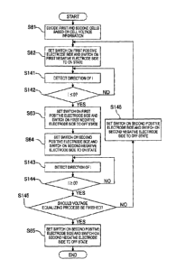
FIG. 14 is a flowchart showing an operation example of the power storage
device 100 of the present embodiment. The operation example shown in FIG 14
includes an embodiment of the power storage control method according to the
present
disclosure.
[0100]
The operation example of FIG. 14 includes the following differences from
FIG. 6. That is, in FIG 14, Step 141 (S141) and Step 142 (S142) are executed
between Step 62 (S62) and Step 63 (S63). In addition, in FIG. 14, Step 143
(S143)
to Step 146 (S146) are executed after Step 64 (S64).
[0101]
Specifically, in Step 141 (S141), the resonance current direction detection
unit 180 detects a direction of the resonance current i.
[0102]
In Step 142 (S142), the power storage control device 130 determines whether
or not i.e., the
direction of the resonance current i has changed, based on the
detection result of Step 141 (S141). Then, when a positive determination
result is
obtained in Step 142 (S142), the power storage control device proceeds to Step
63
(S63), and when a negative determination result is obtained, the power storage
control
device returns to Step 141 (S141).
[0103]
In Step 143 (S143), the resonance current direction detection unit 180 detects
a direction of the resonance current i.
[0104]
In Step 144 (S144), the power storage control device 130 determines whether
or not 1>0, i.e., the direction of the resonance current i has changed, based
on the
detection result of Step 143 (S143). Then, when a positive determination
result is
obtained in Step 144 (S144), the power storage control device proceeds to Step
145
(S145), and when a negative determination result is obtained, the power
storage
control device returns to Step 143 (S143).
[0105]
In Step 145 (S145), the power storage control device 130 determines whether
the voltage equalizing process should be finished. This determination can be
made
CA 02923589 2016-03-07
based on, for example, whether or not an external control signal is input to
the power
storage control device 130, whether a voltage difference between a first cell
and a
second cell is within prescribed values, or the like. Then, when a positive
determination result is obtained in Step 145 (S145), the power storage control
device
5 proceeds to Step 65 (S65), and when a negative determination result is
obtained, the
power storage control device returns to Step 146 (S146).
[0106]
In Step 146 (S146), the power storage control device 130 switches the switch
on the second positive electrode side and the switch on the second negative
electrode
10 side to an off state, and proceeds to Step 62 (S62).
[0107]
As long as the voltage equalizing process is repeated a plurality of times,
i.e.,
a plurality of cycles, when necessary, and energy is transferred between cells
equal in
number in each cycle, transfer of energy between cells of which the numbers
are
15 different in different cycles belongs to the scope of the present
disclosure.
[0108]
According to the power storage device 100 of the present modified example,
a timing at which movement of energy between the first cell or the second cell
and the
series resonance circuit 120 is deemed to have been completed can be detected
using a
20 simple method such as one with respect to a change of a direction of a
current, and the
cell can be disconnected from the series resonance circuit 120. Accordingly, a
more
rapid voltage equalizing process is possible at a low cost. In addition, the
resonance
current direction detection unit 180 can detect a direction of a resonance
current
rapidly and accurately.
25 [0109]
<8. Fourth embodiment>
[Device configuration example]
A power storage device 100 of the present embodiment has a different timing
at which connection of a cell and a series resonance circuit 120 is switched
from the
30 power storage devices 100 of FIGS. 8 and 12. Details thereof will be
described
below.
[0110]
A power storage control device 130 of the present embodiment is configured
CA 02923589 2016-03-07
31
to disconnect a second cell from the series resonance circuit 120 and then to
maintain
a disconnection state of all cells from the series resonance circuit 120
during a set
period (hereinafter referred to as a waiting period). In addition, the power
storage
control device 130 is configured to determine whether or not transfer of
energy, i.e., a
voltage equalizing process, should be finished based on a voltage of a cell
during the
waiting period.
[0111]
A form of the waiting period is not limited, and a proper time can be set for
the power storage control device 130 for measurement of a voltage of a cell
and
determination of appropriateness of the voltage equalizing process. The
waiting
time may be changeable.
[0112]
[Device operation example]
[Time charts]
FIG. 15 is a diagram showing an operation example of the power storage
device 100 of the present embodiment using similar time charts to those of
FIG. 11.
[0113]
In the time charts of FIG. 15, after the switch SW2 is switched off at the
time
t3, the switch SW1 is switched on at a time t4 at which a waiting time T has
elapsed
therefrom. During the waiting time T, the power storage control device 130
determines whether the voltage equalizing process should be finished based on
a
detection result of a cell voltage. Since the resonance current i is OA during
the
waiting time T, the cell voltage measured during the waiting time T has an
accurate
value that is not affected by internal impedance of the cell. If
appropriateness of
finishing the voltage equalizing process is determined based on such an
accurate cell
voltage, a proper determination result can be obtained. Note that, when the
voltage
equalizing process is determined to be finished during the waiting period T,
the power
storage control device 130 does not switch the switch SW1 on at the time t4.
[0114]
[Flowchart]
FIG. 16 is a diagram showing the operation example of the power storage
device 100 of the present embodiment in a flowchart. The flowchart of FIG 16
has a
different process after Step 144 (S144) from the flowchart of FIG 14.
Specifically,
CA 02923589 2016-03-07
32
in FIG 16, after a positive determination result is obtained in Step 144
(S144), Step
65 (S65), Step 161 (S161), and Step 162 (S162) are executed in order.
[0115]
Specifically, in Step 161 (5161), the power storage control device 130 waits
for next connection of a first cell to the series resonance circuit 120 for
the waiting
period and measures a cell voltage during the waiting period. The cell voltage
detection units 150a and 150b shown in FIG. 4 may be caused to measure the
cell
voltage.
[0116]
In Step 162 (S162), the power storage control device 130 determines whether
or not the voltage equalizing process should be finished based on the
measurement
result of the cell voltage in Step 161 (S161). Then, when a positive
determination
result is obtained in Step 162 (S162), the power storage control device
finishes the
process, and when a negative determination result is obtained, the power
storage
control device proceeds to Step 62 (S62).
[0117]
According to the present embodiment, appropriateness of finishing the
voltage equalizing process can be properly determined based on an accurate
cell
voltage measured during a waiting period, and further, the voltage equalizing
process
can be performed more suitably.
[0118]
<9. First modified example of the fourth embodiment>
[Device configuration example]
A power storage device 100 of the present embodiment has a different timing
at which connection of a cell and a series resonance circuit 120 is switched
from the
power storage device 100 of FIGS. 15 and 16. Details thereof will be described
below.
[0119]
A power storage control device 130 of the present embodiment is configured
to maintain a disconnection state of all cells from the series resonance
circuit 120
during a waiting period even after a first cell is disconnected from the
series
resonance circuit 120, and to determine appropriateness of finishing a voltage
equalizing process during the waiting period. This waiting period may also be
set to
CA 02923589 2016-03-07
33
be changeable with respect to the power storage control device 130.
[0120]
[Device operation example]
[Time charts]
FIG. 17 includes time charts showing an operation example of the power
storage device 100 of the present embodiment. In the time charts of FIG 17,
after
the switch SW1 is switched off at the time t2, the switch SW2 is switched on
at the
time t3 at which a second waiting period T2 has elapsed. In addition, in the
time
charts of FIG 17, after the switch SW2 is switched off at the time t4, the
switch SW!
is switched on at a time t5 at which a first waiting period T1 has elapsed.
During the
waiting periods Ti and T2, the power storage control device 130 determines
whether
or not the voltage equalizing process should be finished based on a detection
result of
a cell voltage. The waiting periods Ti and T2 may be the same as or different
from
each other.
[0121]
[Flowchart]
FIG 18 is a flowchart showing the operation example of the power storage
device 100 of the present embodiment. The flowchart of FIG 18 is different
from
the flowchart of FIG 16 in that Step 181 (S181) and Step 182 (S182) are
executed
between Step 63 (S63) and Step 64 (S64).
[0122]
Specifically. in Step 181 (S181), the power storage control device 130 waits
for connection of a second cell to the series resonance circuit 120 for the
second
waiting period and measures a cell voltage during the second waiting period.
[0123]
In Step 182 (S182), the power storage control device 130 determines whether
or not the voltage equalizing process should be finished based on the
measurement
result of the cell voltage of Step 181 (S181). Then, when a positive
determination
result is obtained in Step 182 (S182), the power storage control device
finishes the
process, and when a negative determination result is obtained, the power
storage
control device proceeds to Step 64 (S64).
[0124]
According to the power storage device 100 of the present modified example,
CA 02923589 2016-03-07
34
it is possible to increase chances of accurately determining appropriateness
of
finishing the voltage equalizing process.
[0125]
<10. Fifth embodiment>
[Device configuration example]
FIG. 19 is a diagram showing a configuration example of a series resonance
circuit 120 of a power storage device 100 of the present embodiment. The
series
resonance circuit 120 of the present embodiment is different from the series
resonance
circuits 120 of the first to fourth embodiments in that it has a resistance
123, in
.. addition to a reactor 121 and a capacitor 122. In other words, the series
resonance
circuit 120 of the present embodiment is an RLC series resonance circuit.
[0126]
[Device operation example]
An operation example of the power storage device 100 of the present
embodiment can be described as an operation example of an equivalent circuit
of the
power storage device 100 shown in FIG. 20.
[0127]
With respect to the equivalent circuit of FIG. 20, the peak value Ipeak [A] of
a resonance current i flowing in a first cell (Ce111) and a second cell
(Ce112) is a value
indicated by the following expression (I).
Ipeak = (El¨E2)/(2xR) (1)
In the expression (1), El represents a voltage [V] of the first cell. E2
represents a voltage [V] of the second cell. R represents a value [0] of the
resistance 123.
[0128]
As the expression (1) indicates, the peak value Ipeak varies according to a
value of the resistance 123, and as a resistance value increases, a smaller
peak value
Ipeak is obtained.
[0129]
The resonance current i [A] is a value indicated by the following expression
(2).
i = {(El¨E2)/(2xR)Ixsinwot (2)
In the expression (2), coo represents a resonance angle frequency [rad/s]
CA 02923589 2016-03-07
expressed by the following expression (3).
coo = 1/(LxC)1/2 (3)
In the expression (3), L represents a self-inductance [H] of the reactor 121,
and C represents electrostatic capacitance [F] of the capacitor 122.
5 Note that a resonance frequency fo is coo/27c from the expression (3).
[0130]
In the expression (2), in a first-half cycle, i.e., in a period in which coot
is 0 to
IT [rad], discharge is performed from the first cell to the series resonance
circuit 120.
On the other hand, in a second-half cycle, i.e., in a period in which coot is
71 to 271 [rad],
10 charge is performed from the series resonance circuit 120 to the second
cell. The
average discharge current Idis [A] of the first-half cycle and the average
charge
current Icha [A] of the second-half cycle can be obtained by integrating the
expression (2) for each half cycle of a resonance frequency and averaging the
results.
Specifically, the average discharge current Idis and the average charge
current Icha
15 have a value expressed by the following expression (4).
Icha = Idis = (E 1¨E2)/(nxR) (4)
If connection of a cell and the series resonance circuit 120 is switched at a
timing at which i is OA or a timing at which the direction of i changes,
electric charge
corresponding to the expression (4) can be supplied from the first cell to the
second
20 cell.
[0131]
According to the power storage device 100 of the present embodiment, since
the peak current Ipeak can be suppressed by the resistance 123, a burden
imposed on a
cell can be more effectively reduced.
25 [0132]
<11. First modified example of the fifth embodiment>
FIG. 21 is a diagram showing a main part of a power storage device 100 of
the present modified example. The power storage device 100 of the present
modified example is configured such that a power storage control device 130
detects
30 the direction and magnitude of a current flowing in a series resonance
circuit 120
based on a potential difference of both ends of a resistance 123 of the series
resonance
circuit 120. The potential difference of both ends of the resistance 123 may
be
detected by a voltage detection unit 190.
CA 02923589 2016-03-07
36
[0133]
According to the power storage device 100 of the present modified example,
costs can be reduced more even when the resonance current detection unit 170
of FIG.
8 and the resonance current direction detection unit 180 of FIG. 12 are
provided to
detect a resonance current.
[0134]
<12. Second modified example of the fifth embodiment>
FIG. 22 is a diagram showing a series resonance circuit 120 of a power
storage device 100 of the present modified example. The series resonance
circuit
120 of FIG 22 is different from the series resonance circuit 120 of FIG. 19 in
that a
resistance 123 is a parasitic resistance. The parasitic resistance may be a
parasitic
resistance of at least one of a reactor 121, a circuit wire, and a switch.
According to
the present modified example, a peak value of a resonance current can be
suppressed
using a small number of parts.
[0135]
<13. Sixth embodiment>
[Device configuration example]
A power storage device 100 of the present embodiment has a different
configuration for switching connection of a cell and a series resonance
circuit 120
from the power storage devices 100 of the first to fifth embodiments. Details
thereof
will be described below.
[0136]
A power storage control device 130 of the present modified example is
configured to switch connection of the series resonance circuit 120 and a cell
using a
resonance frequency of the series resonance circuit 120.
[0137]
Here, like the period between the time ti and the time t2 of FIG 11, a period
from connection of one cell to the series resonance circuit 120 to connection
of
another cell replacing the one cell to the series resonance circuit 120 is
defined as a
connection switching cycle. Since the connection switching cycle is a half
cycle of a
resonance cycle of the series resonance circuit 120, it is indicated with
rc(LxC)1/2 [s].
The power storage control device 130 of the present modified example can be
said to
be configured to switch connection of the series resonance circuit 120 and a
cell in
CA 02923589 2016-03-07
37
each connection switching cycle.
[0138]
The power storage control device 130 may be configured to store
information such as a resonance frequency and a connection switching cycle,
and to
operate by computing a connection switching timing based on the stored
information.
[0139]
[Device operation example]
FIG. 23 is a flowchart showing an operation example of the power storage
device 100 of the present embodiment. In FIG. 23, first, the power storage
control
device 130 connects a cell on a power supply side to the series resonance
circuit 120
in Step 231 (S231).
[0140]
Next, in Step 232 (S232), the power storage control device 130 determines
whether or not a connection switching timing based on a resonance frequency of
the
series resonance circuit 120 has arrived. Then, when a positive determination
result
is obtained in Step 232 (S232), the power storage control device proceeds to
Step 233
(S233), and when a negative determination result is obtained, the power
storage
control device returns to Step 232 (S232).
[0141]
Next, in Step 233 (S233), the power storage control device 130 disconnects
the cell on the power supply side from the series resonance circuit 120.
[0142]
Next, in Step 234 (S234), the power storage control device 130 connects a
cell on a power reception side to the series resonance circuit 120.
[0143]
Next, in Step 235 (S235), the power storage control device 130 determines
whether or not a connection switching timing based on a resonance frequency of
the
series resonance circuit 120 has arrived. Then, when a positive determination
result
is obtained in Step 235 (S235), the power storage control device proceeds to
Step 236
(S236), and when a negative determination result is obtained, the power
storage
control device repeats Step 235 (S235).
[0144]
Next, in Step 236 (S236), the power storage control device 130 disconnects
CA 02923589 2016-03-07
38
the cell on the power reception side from the series resonance circuit 120.
[0145]
Then, in Step 237 (S237), the power storage control device 130 finishes this
voltage equalizing process when the process should be finished, and returns to
Step
231 (S231) when the voltage equalizing process is to be continued. The
determination of whether to finish the voltage equalizing process may be
performed
before Step 237 (S237).
[0146]
According to the power storage device 100 of the present embodiment,
connection of a cell can be switched at a timing proper for transfer of
energy, with no
need to monitor a current flowing in the series resonance circuit 120.
[0147]
<14. Seventh embodiment>
The power storage device 100 of the present embodiment shows a different
resonance frequency of the series resonance circuit 120 from the power storage
devices 100 of the first to sixth embodiments.
[0148]
Specifically, the resonance frequency of the series resonance circuit 120
according to the present embodiment is a frequency when an imaginary number
component in a Cole-Cole plot of internal impedance of cells measured using an
AC
impedance method is 0.
[0149]
Here, in the AC impedance method, the internal impedance of each
frequency is measured while a frequency is changed by applying an alternate
current
to cells. The Cole-Cole plot is one method for illustrating a measurement
result of
the AC impedance method. In the Cole-Cole plot, the internal impedance of
cells for
each frequency obtained using the AC impedance method is plotted on a complex
plane whose horizontal axis represents real number components of internal
impedance
and whose vertical axis represents imaginary number components of the internal
impedance.
[0150]
An example of the Cole-Cole plot is shown in FIG. 24. The horizontal axis
of FIG 24 represents the real part of internal impedance of a cell, and the
vertical axis
CA 02923589 2016-03-07
39
of FIG. 24 represents the imaginary part of the internal impedance of the
cell. In FIG
24, the frequency when an imaginary component of the internal impedance
becomes 0
is fmin [Hz]. In this case, the series resonance circuit 120 may be designed
so that
fmin serves as a resonance frequency. Specifically, it is preferable to select
the self-
inductance L of the reactor 121 and the electrostatic capacitance C of the
capacitor
122 in advance to satisfy fmin = 1/{2nx(LxC)1/2}. Note that fmin may be a
value of
lk [Hz] to 10k [Hz].
[0151]
In the power storage device 100 of the present embodiment, internal
impedance of a cell becomes the minimum with respect to a current flowing
between
a cell and the series resonance circuit 120. Therefore, energy can be
efficiently
transferred.
[0152]
<15. First modified example of the seventh embodiment>
A power storage device 100 of the present modified example has a different
setting of a resonance frequency of series resonance circuit 120 from the
power
storage device 100 described with reference to FIG. 24.
[0153]
Examples of Cole-Cole plots for describing the power storage device 100 of
the present modified example are schematically shown in FIG. 25. The
horizontal
axis Z' of FIG 25 represents the real part of internal impedance of cells and
the
vertical axis Z" of FIG 25 represents the imaginary part of the internal
impedance of
the cells. In FIG. 25, the Cole-Cole plots of respective states of charge
(SOC) [ /0]
are shown as examples of charge ratios of cells. The Cole-Cole plots of FIG.
25 are
plots based on measurement results of the internal impedance of the cells by a
frequency response analyzer (FRA). Specific numerical values in FIG 25 are
merely
examples, and do not limit the scope of the present disclosure.
[0154]
As shown in FIG. 25, a Cole-Cole plot may be different according to SOC.
When the frequency fmin when the imaginary number component in the Cole-Cole
plot is 0 is different according to SOC, fmin is obtained for each SOC and a
resonance
frequency of the series resonance circuit 120 may be set comprehensively
taking
obtained fmin of each SOC into consideration. For example, the series
resonance
CA 02923589 2016-03-07
circuit 120 may be designed such that the average value of fmin of the SOC is
obtained and the average value is set to the resonance frequency.
[0155]
According to the present modified example, energy can be efficiently
5 transferred in consideration of a changing SOC.
[0156]
<16. Eighth embodiment>
A power storage device 100 of the present embodiment has a specific cell
with respect to the power storage devices 100 of the first to seventh
embodiments.
10 [0157]
Specifically, a cell of the present embodiment has a discharge characteristic
in which a change of a voltage is 0.25 V or lower in a series of sections
spanning 50%
or more of the section of the charge ratio of 0% to 100%.
[0158]
15 As an example of such a discharge characteristic, a discharge curve
obtained
when a lithium ion secondary battery of which a material of the positive
electrode is
olivine-type iron phosphate is discharged at 1C is shown in FIG 26. With
respect to
the discharge curve of FIG. 26, the horizontal axis represents SOC [%] as an
example
of a discharge ratio, and the vertical axis represents terminal voltages [V]
of cells. In
20 the discharge curve of FIG. 26, a change of voltage is 0.25 V or lower
in a series of
sections spanning 50% or more of the section of the discharge ratio of 0% to
100%.
More specifically, the discharge curve of FIG. 26 shows a change of voltage of
about
0.1 V in the section of the discharge ratio of 20% to 90%. Although the
discharge
curve of FIG. 26 shows a significant voltage drop attributable to internal
resistance
25 immediately after the start of discharge, it continuously shows a flat
characteristic
thereafter, and thus unevenness in voltage within a battery pack configured in
serial
connection becomes small. The cells are not limited to lithium ion secondary
batteries that use olivine-type iron phosphate.
[0159]
30 Here, the power storage device 100 has relatively even temperature
distribution therein and a load current fluctuates little in comparison to an
automobile
or the like, and thus unevenness of voltages between cells is small.
Therefore, in the
power storage device 100, it is desirable in the voltage equalizing process to
secure
CA 02923589 2016-03-07
41
cell balance with a low current without waste, rather than rapidly resolving
unevenness of voltages between cells using a high current. In addition,
if a cell
having a flat discharge characteristic as in the present embodiment is
applied,
effectiveness of a voltage equalizing process can be secured with a low
current.
[0160]
The above-described embodiments and modified examples may be
appropriately combined.
[0161]
Effects described in the embodiments and modified examples are merely
illustrative and are not limitative, and other effects may be exhibited. The
present
disclosure may exhibit any one of a plurality of effects described in the
embodiments
and modified examples.
[0162]
Additionally, the present technology may also be configured as below.
(1)
A power storage device including:
a plurality of cells which are connected in series;
a series resonance circuit configured to include a reactor and a capacitor;
and
a power storage control device configured to control a connection state of the
.. cells and the series resonance circuit,
wherein the power storage control device causes energy to be transferred
between equal numbers of cells via the series resonance circuit.
(2)
The power storage device according to (1), wherein, after the power storage
control device connects first cells including at least one cell to the series
resonance
circuit, the power storage control device connects second cells which include
cells
equal in number to the first cells and have a lower total voltage than the
first cells to
the series resonance circuit.
(3)
The power storage device according to (2), wherein the power storage
control device selects a plurality of consecutive cells as the first cells,
and selects
consecutive cells equal in number to the first cells as the second cells.
(4)
CA 02923589 2016-03-07
42
The power storage device according to (2) or (3), wherein, when the first
cells are connected to the series resonance circuit and then the direction of
a current
flowing in the series resonance circuit changes, the power storage control
device
disconnects the first cells from the series resonance circuit.
.. (5)
The power storage device according to (4), wherein, when the second cells
are connected to the series resonance circuit and then the direction of a
current
flowing in the series resonance circuit changes, the power storage control
device
disconnects the second cells from the series resonance circuit.
.. (6)
The power storage device according to (5), wherein the power storage
control device maintains a state in which all the cells are disconnected from
the series
resonance circuit during a set period after the first and/or second cells are
disconnected from the series resonance circuit, and determines whether or not
transfer
.. of energy is to be finished based on a voltage of the cells during the set
period.
(7)
The power storage device according to any one of (1) and (4) to (6),
wherein the series resonance circuit includes a resistance, and
wherein the power storage control device detects the direction of a current
flowing in the series resonance circuit based on a potential difference of
both ends of
the resistance.
(8)
The power storage device according to any one of (1) to (3), wherein the
power storage control device switches connection of the series resonance
circuit and
the cells using a resonance frequency of the series resonance circuit.
(9)
The power storage device according to any one of (1) to (8), wherein a
resonance frequency of the series resonance circuit is a frequency when an
imaginary
component in a Cole-Cole plot of internal impedances of the cells measured
using an
.. AC impedance method becomes 0.
(10)
The power storage device according to any one of (2) to (9), wherein the
power storage control device causes a cell having a maximum voltage to be
included
CA 02923589 2016-03-07
43
in the first cells.
(11)
The power storage device according to any one of (2) to (10), wherein the
power storage control device causes a cell having a minimum voltage to be
included
in the second cells.
(12)
The power storage device according to any one of (1) to (11), further
including:
a switch configured to connect or disconnect the cells and the series
resonance circuit,
wherein the power storage control device controls a connection state of the
cells and the series resonance circuit by controlling an operation of the
switch.
(13)
The power storage device according to any one of (1) to (12), wherein the
cells have a discharge characteristic that a change of a voltage is 0.25 V or
lower in a
series of sections spanning 50% or more of a section of a charge ratio of 0%
to 100%.
(14)
A power storage program for causing a computer to functions as a means of
controlling a connection state of a plurality of cells which are connected in
series and
a series resonance circuit which includes a reactor and a capacitor and
causing energy
to be transferred between equal numbers of cells via the series resonance
circuit.
Reference Signs List
[0163]
100 power storage device
110a, 110b cell
120 series resonance circuit
121 reactor
122 capacitor
130 power storage control device