Note: Descriptions are shown in the official language in which they were submitted.
CA 02923940 2016-03-10
1
Antenna for short-range applications and use of such an antenna
The present invention relates to the field of high-frequency technology,
particularly an
antenna for short-range applications, such as RFID applications, for example.
Further-
more, the invention relates to the use of such an antenna.
In the sense of the invention, the term "short-range applications" in
particular comprises
applications in which the transmission of electromagnetic energy and/or
electromagnetic
signals is provided with the use of the antenna over distances which are
smaller than 5
m, in particular smaller than 1 m. However, this distance is preferably
greater than 0.01
m, particularly greater than 0.05 m.
It is an object of the present invention to realise a wireless and reliable
transmission of
energy and/or information, particularly over short distances, in a simple
manner.
This object is achieved according to a first aspect of the invention by an
antenna, which
comprises an elongated bipolar conductor structure with an inner conductor and
an en-
velope conductor coaxially surrounding the same, wherein a first end of the
conductor
structure is provided as a connection end for connecting a transmitter and/or
receiver for
an antenna signal to be transmitted using the antenna or an antenna signal to
be re-
ceived by the antenna, and wherein an inner-conductor extension, which is
connected to
the inner conductor, is provided at a second end of the conductor structure
and a free
end of the inner-conductor extension is capacitively coupled to the envelope
conductor.
Using this relatively simple design according to the invention, broadband
coaxial travel-
ling-wave antennas for short-range applications can advantageously be
realised, as ex-
plained in the following.
The term "travelling wave" here relates to a preferred operating mode of the
antenna in
the context the invention, in which e.g. during transmission starting from the
second end
of the coaxial conductor structure, electromagnetic waves run back along the
conductor
structure in the direction towards the first end of the conductor structure.
CA 02923940 2016-03-10
2
This functionality of the antenna in transmission mode, i.e. when feeding in a
high-
frequency transmit signal at the connection end (first end) can be described
as follows:
The transmit signal applied and thus fed in at the first end of the conductor
structure,
between inner conductor and envelope conductor, is in principle, such as e.g.
in the case
of a conventional "coaxial cable", transmitted along the coaxial conductor
structure to the
second end thereof. The discontinuity of the conductor structure created by
the second
end in connection with the capacitive coupling of the inner-conductor end to
the enve-
lope conductor via the inner-conductor extension provided at this point
effects the afore-
mentioned running back of electromagnetic travelling waves as surface waves
along the
io conductor structure (on the exterior of the envelope conductor) in the
direction of the first
end of the conductor structure.
For many interesting applications, it is advantageous here if the antenna
builds up an
electromagnetic field (travelling waves) around itself to some extent, but
only radiates
very little or absolutely no electromagnetic energy (by means of
electromagnetic waves
that "detach" themselves). An operating mode of this type is termed a "coupled
mode"
here.
According to an embodiment of a "coupled-mode" operating method of an antenna
ac-
cording to the invention, it is e.g. provided that in transmission mode, more
than 50% of
the energy arriving at the second end of the conductor structure due to the
feeding in of
the transmit signal runs as a travelling wave "bound on the conductor
structure" emanat-
ing from the second end (back in the direction of the first end). In this
case, less than
50% of the energy arriving at the second end is consequently radiated from the
antenna
as an electromagnetic wave.
Alternatively or additionally, in the "coupled-mode" operating method of an
antenna ac-
cording to the invention, it can e.g. be provided that in transmission mode,
more than
40% of the energy fed in at the first end (connection end) of the conductor
structure due
to the feeding in of the transmit signal runs as a travelling wave bound on
the conductor
structure emanating from the second end (back in the direction of the first
end).
The antenna according to the invention has an elongated conductor structure.
This con-
ductor structure can be stiff or flexible. It is also possible that both at
least one stiff sec-
CA 02923940 2016-03-10
3
tion and at least one flexible section are provided, of which the conductor
structure is
composed. The length of the elongated conductor structure can be larger than a
(maxi-
mum) transverse extent (e.g. diameter) of the conductor structure e.g. by a
factor in the
range from 10 to 50,000.
The length of the elongated conductor structure can be e.g. at least 0.05 m,
in particular
at least 0.1 m. However applications in which this length is substantially
larger are par-
ticularly interesting. For most applications it is satisfactory however, if
this length is at
most 200 m, particularly at most 100 m.
In an embodiment, it is provided that the length of the elongated conductor
structure (or
the length of a signal transmitter/receiver section which is further described
below) is at
least 2-times, particularly at least 5-times the wavelength of the travelling
waves men-
tioned provided during operation.
In an embodiment, it is provided that the latter length at a signal frequency
of up to 1
GHz provided during operation is at most 500-times, in particular at most 300-
times the
corresponding wavelength. For operating frequencies of more than 1 GHz, it is
provided
according to one embodiment that this length is at most 1,000-times, in
particular at most
500-times the corresponding operational wavelength of the travelling waves.
The antenna according to the invention is preferably used with an operating
frequency
(carrier frequency of the antenna signal in transmission mode) in the range of
400 MHz
to 6 GHz. In an embodiment, the operating frequency lies e.g. in the range
from 860 to
960 MHz (as is conventional e.g. for many RFID applications). In a different
embodiment,
an operating frequency in the range from 1 to 3 GHz, for example 2.4 GHz, is
used.
The inner conductor and the envelope conductor are electrically conductive
(e.g. made
from metal). In the simplest case, the inner conductor has a circular cross
section and
the envelope conductor has an annular cross section.
In a departure from circular cross-sectional contours, different cross-
sectional contours
for the inner conductor and/or the envelope conductor are also possible, for
example
rectangular or square or oval shapes.
CA 02923940 2016-03-10
4
The inner conductor can be formed solidly or as a hollow conductor.
The cross section of the inner conductor and/or the cross section of the
envelope con-
ductor are uniform in the simplest case, when considered over the length of
the conduc-
tor structure.
As observed in the radial direction, electrical insulation or a dielectric
(including e.g. air)
can be arranged between inner conductor and envelope conductor. Electrical
insulation
(e.g. made from plastic), also termed "insulating sheath" in the following, is
preferably
provided radially outside of the envelope conductor, which like the inner
conductor can
preferably be formed from a metallic material.
The inner-conductor extension is a structure, which is electrically connected
to the inner
conductor at the second end of the conductor structure and is used in
transmission mode
of the antenna for "decoupling" energy out of the inner conductor and
"coupling" this en-
ergy into the envelope conductor.
The inner-conductor extension is an electrical conductor in the simplest case,
which on
the one hand is connected to the inner conductor and a free end of which on
the other
hand preferably projects relatively close to the envelope conductor, in order
to realise the
capacitive coupling to the envelope conductor.
In a development it is provided that the inner-conductor extension has at
least one ca-
pacitive, inductive or resistive element in the run between inner conductor
and envelope
conductor.
In a preferred embodiment, the inner-conductor extension runs outside of the
envelope
conductor at least to some extent.
In an embodiment, the inner-conductor extension has at least one angled
section of the
run and/or at least one curved section of the run emanating from the second
end of the
conductor structure up to the free end of the inner-conductor extension.
CA 02923940 2016-03-10
In an embodiment, the free end of the inner-conductor extension is
capacitively coupled
to the exterior of the envelope conductor. Alternatively or additionally, a
capacitive cou-
pling to the inside and/or the front side (at the conductor structure end) of
the envelope
conductor is conceivable.
5
In an embodiment, the inner-conductor extension is formed to be integrally
connected to
the inner conductor. In a different embodiment, the inner-conductor extension
is formed
separately from the inner conductor, but connected to the same.
io In a preferred embodiment, as viewed in the longitudinal direction of
the conductor struc-
ture, a surface-wave damping device is arranged at a distance from the second
end of
the conductor structure, for example on the outer circumference of the
envelope conduc-
tor (e.g. surrounding an insulating sheath).
A surface-wave damping device of this type is advantageous insofar as the
region of the
"returning travelling waves" mentioned can be delimited in a well-defined
manner along
the conductor structure. The damping device is used to absorb the energy of
arriving
returning travelling waves, at least for the most part. In an embodiment, the
damping
device has at least one ferrite ring for this, which surrounds the outer
circumference of
the envelope conductor. In particular, a plurality of ferrite rings can also
be arranged one
behind the other in the longitudinal direction of the conductor structure,
which in each
case surround the outer circumference of the envelope conductor (with or
without mutual
spacing). In a development, the ferrite ring (or at least one of a plurality
of ferrite rings) is
displaceably attached on the conductor structure.
Alternatively or additionally to at least one ferrite ring surrounding the
envelope conduc-
tor, the surface-wave damping device can also have a damping unit comprising a
damp-
ing network (made up of capacitive and/or inductive and/or resistive elements)
inter-
posed in the run of the elongated bipolar coaxial conductor structure.
In an embodiment, the surface-wave damping device comprises an earth of the
envelope
conductor. An earth of this type can be implemented e.g. by means of an
"earthing
sleeve" attached on the outer circumference of the envelope conductor. An
earthing
CA 02923940 2016-03-10
6
sleeve of this type can be formed e.g. in a divided manner from two earthing-
sleeve
halves, which are connected to one another (e.g. screwed) for fitting.
If a surface-wave damping device is provided, then the total length of the
coaxial conduc-
tor structure is therefore divided into a "signal-conducting section", located
between the
first end of the conductor structure and the damping device, and a "signal
transmit-
ter/receiver section", located between the damping device and the second end
of the
conductor structure. In a development of the invention, it is provided that
one or a plurali-
ty of "discontinuities" (significant local deviations of a wave impedance
effective for the
io travelling waves) are provided inside the signal transmitter/receiver
section. Each discon-
tinuity of this type can be implemented e.g. likewise by means of a ferrite
ring as already
described or a similar device. The advantage of this development consists in
the fact that
the propagation of the travelling waves along the conductor structure can be
influenced
thereby in a desired manner (for example for "wave shaping").
In the case of a relatively long antenna according to the invention, the
arrangement of a
surface-wave damping device may be dispensable insofar as the travelling waves
run-
ning back from the second to the first conductor structure end no longer have
too great
an intensity, due to the unavoidable intensity loss, if the travelling waves
reach the vicini-
ty of the first end. However, in this case also, the previously mentioned
discontinuities,
e.g. implemented by means of ferrite rings or the like, at one or a plurality
of points in the
run of the antenna may be advantageous in order to influence the wave
propagation in a
targeted manner.
As already mentioned, a preferred use of the antenna according to the
invention consists
in using the same as a travelling-wave antenna in a "coupled mode". This use
according
to the invention can be provided e.g. for communication with transponders
located in the
surroundings of the antenna and/or for communication with components of a
computer
network located in the surroundings of the antenna.
In the "coupled-mode" operating method, communication can take place in
particular not
by means of electromagnetic radiation in the narrower sense, but rather by
means of
wave coupling with systems or units located within the antenna range. A
wireless energy
CA 02923940 2016-03-10
7
supply of such systems or units (e.g. sensors, particularly "intelligent
sensors") can also
be implemented as an alternative or in addition to wireless communication.
In a development of the invention, a "modular design" of the antenna is
provided, which
can be realised in particular in that one or a plurality of electrical
contacts (e.g. plug
and/or screw connections) are provided in the run from the first end of the
conductor
structure to the second end of the conductor structure (or the inner-conductor
extension
attached on the second end), which correspondingly delimit individual
"modules", of
which the antenna is composed.
In a corresponding embodiment, it is provided that a surface-wave damping
device of the
previously described type is equipped at one or at both of its ends with a
corresponding
connector device (e.g. electric plug or the like). Alternatively or
additionally, a connector
device of this type can in particular also be provided at the second end of
the conductor
structure for connecting the inner-conductor extension. The inner-conductor
extension
can accordingly be equipped with a (counterpart) connector device.
A major advantage of a modular design of the antenna of this type consists
e.g. in it be-
ing possible to some extent to use conventional and already commercially
available
components such as e.g. "coaxial cables" to build the antenna, which are only
to be sup-
plemented with the respectively required additional modules for the
construction accord-
ing to the invention of an antenna. In particular, a conventional coaxial
cable can be used
in order to form the coaxial conductor structure provided according to the
invention. If a
surface-wave damping device is provided, this can be formed e.g. by means of a
corre-
sponding damping module, which is supplemented on both sides with conventional
coax-
ial cables (e.g. via conventional electrical plug/screw connections), in order
to realise the
signal cable section on the one hand and the signal transmitter/receiver
section of the
antenna on the other hand by means of the two coaxial cables.
The invention is described further in the following on the basis of exemplary
embodi-
ments with reference to the attached drawings. In the figures:
Fig. 1 shows an antenna according to a first exemplary embodiment,
CA 02923940 2016-03-10
8
Fig. 2 shows an antenna according to a further exemplary embodiment,
Fig. 3 shows an antenna according to a further exemplary embodiment,
Fig. 4 shows the antenna from Fig. 2, illustrated in a particular
application situation,
Fig. 5 shows an antenna according to a further exemplary embodiment,
Fig. 6 shows an antenna according to a further exemplary embodiment,
illustrated in
a plan view,
Fig. 7 shows the antenna from Fig. 6, illustrated in a schematic side
view, and
Fig. 8 shows an antenna according to a further exemplary embodiment in an
illus-
tration corresponding to Fig. 7.
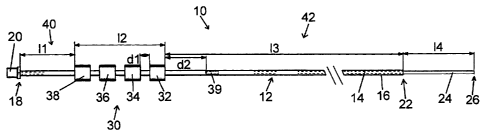
Fig. 1 shows an antenna 10 according to a first exemplary embodiment provided
for
short-range applications, particularly e.g. RFID applications.
The antenna 10 comprises an elongated bipolar coaxial conductor structure 12
with an
electrically conductive inner conductor 14 and an electrically conductive
envelope con-
ductor 16 coaxially surrounding the inner conductor 14.
In the exemplary embodiment illustrated, the inner conductor 14 is cylindrical
and the
envelope conductor 16 is hollow and cylindrical. The inner conductor 14 like
the enve-
lope conductor 16 is e.g. in each case formed from a metallic material,
wherein an elec-
trically insulating intermediate layer (e.g. made from plastic) is expediently
present radi-
ally between the inner conductor and the envelope conductor 16 over the entire
length of
the conductor structure 12.
A first end 18 of the conductor structure 12 (on the left in Fig. 1) is
provided for connect-
ing a transmitter and/or receiver for an antenna signal to be transmitted
using the anten-
na 10 or an antenna signal to be received by the antenna 10, respectively, and
is provid-
ed with a conventional coaxial plug 20 for this in the example illustrated,
which coaxial
CA 02923940 2016-03-10
9
plug realises an electrical connector for the inner conductor 14 and for the
envelope
conductor 16 at this first end 18 in the conventional manner for "conventional
coaxial
cables".
An inner-conductor extension 24, which is formed integrally with the inner
conductor 14
in the example illustrated and is therefore electrically connected to the
inner conductor
14, is provided at an opposite second end 22 of the conductor structure 12 (on
the right
in Fig. 1), which inner-conductor extension, in the example illustrated,
extends out of the
envelope conductor 16, starting from the second end 22 of the conductor
structure 12,
io rectilinearly and coaxially to the run of inner conductor 14 and
envelope conductor 16
directly before the second end 22. The inner-conductor extension 24 extends
rectilinear-
ly up to a free end 26 of the inner-conductor extension 24, wherein a certain
capacitive
coupling of the free end 26 or of the inner-conductor extension 24 to the
envelope con-
ductor 16 exists in the region of the second end 22 thereof, depending on the
length of
the inner-conductor extension 24.
In a transmission mode of the antenna 10, that is to say if an antenna signal
to be trans-
mitted is fed in at the coaxial plug 20 of the first end 18, then this antenna
signal runs
along the conductor structure 12 up to the end 22 and is reflected there more
or less
zo strongly, in order to run back as a bound travelling wave emanating from
the second end
22 along the envelope conductor 16 in the direction of the first end 18.
For a correspondingly chosen operating method, for example with regards to the
fre-
quency and power of the antenna signal fed in, it can be achieved that the
antenna 10
builds up an electromagnetic alternating field around itself, but radiates
relatively little.
Rather, it can be achieved that the antenna 10 is operated as a travelling-
wave antenna
in a "coupled mode", in order to therefore have good control over the
(preferably relative-
ly small) range of the antenna 10.
In the example illustrated, a surface-wave damping device 30 is arranged on
the outer
circumference of the envelope conductor 16, at a distance from the second end
22 (or at
a point between the two ends 18 and 22) as viewed in the longitudinal
direction of the
conductor structure 12, which device is formed, in the example illustrated,
from a plurality
(here: four) of ferrite rings 32, 34, 36 and 38, which in each case surround
the outer cir-
CA 02923940 2016-03-10
cumference of the envelope conductor. If an insulating sheath (e.g. made from
plastic) is
expediently provided over the entire length of the conductor structure 12 on
the outer
circumference of the envelope conductor 16, then the ferrite rings 32, 34, 36
and 38 sur-
round this insulating material. The ferrite rings 32 to 38 are arranged
mutually spaced
5 from one another as viewed in the longitudinal direction of the conductor
structure 12
and advantageously effect a damping of the travelling waves mentioned, which
run back
from the second end 22 of the conductor structure 12, when these waves arrive
at the
site of the damping device 30. The damping device 30 formed from the ferrite
rings 32 to
38 or the arrangement location thereof in the run of the coaxial conductor
structure 12
-io therefore divides the total length of the conductor structure 12 into a
"signal-conducting
section" 40 (on the left in Fig. 1) and a "signal transmitter/receiver
section" 42, wherein
during operation of the antenna 10, the section 40 is used for conducting the
antenna
signal emanating from or to the first end 18, and the section 42 is used for
transmitting
information and/or energy emanating from the antenna 10 or to the antenna 10.
The number of ferrite rings and the individual distances between the ferrite
rings can be
adjusted to the respective use case or the operating parameters of the antenna
10. It can
also be provided that at least one ferrite ring, in the case of a plurality of
ferrite rings,
preferably at least the "first" ferrite ring (closest to the second end 22),
that is to say the
ferrite ring 32 in the example illustrated, is arranged such that it can be
displaced along
the conductor structure. Therefore, the properties of the thus formed damping
device can
advantageously be influenced or adapted to the actual use case.
As an alternative or in addition to the ferrite rings 32 to 38, the damping
device 30 can, in
a departure from the example illustrated, also have different damping
components, such
as for example an electric network structure (made up of capacitive and/or
inductive
and/or resistive elements), which is arranged at the relevant point in the run
of the con-
ductor structure 12 and connected on both sides to the sections 40, 42 of the
conductor
structure 12 running to the first end 18 and to the second end 22.
In summary, the structure, functionality and advantages of the antenna 10 can
be out-
lined as follows:
CA 02923940 2016-03-10
11
- A main component of the antenna 10 is formed by the coaxial conductor
structure 12,
which can be e.g. a flexible or semi-rigid cable, or else a stiff structure,
which has an
"open end" or the inner-conductor extension 24 mentioned.
- In the region of the inner-conductor extension 24, an envelope conductor
16 forming a
shielding is removed to a certain extent in the remaining region of the
conductor struc-
ture, so that a dipole antenna is created, one arm of which is formed by the
open in-
ner conductor (inner-conductor extension 24) and the other arm of which is
formed by
the envelope conductor 16.
- The surface-wave damping device 30 formed here by one or a plurality of
ferrite rings
limits the effective antenna length for transmitting/receiving (section 42).
In addition to
an adjustment of this antenna length, the position of the damping device 30,
here the
position of the first ferrite ring 32 in particular, also influences the
properties of the
damping device 30 and therefore the properties of the returning travelling
waves.
- It is generally advantageous with regards to the desired generation of
returning travel-
ling waves if the inner-conductor extension 24 has a length (measured from the
sec-
ond end 22 of the conductor structure 12 to the free end of the inner-
conductor exten-
sion 24) which at least approximately represents a quarter wavelength of the
relevant
antenna signal. A carrier frequency of the antenna signal may lie e.g. in the
range
from 500 to 5000 MHz.
- The actual position of the ferrite rings 32 to 38, particularly of the
first ferrite ring 32,
also strongly influences the impedance of the antenna 10. In this respect, an
adjusta-
bility of at least one, particularly at least the first of a plurality of
ferrite rings can ad-
vantageously be used for impedance adjustment (e.g. as close as possible to 50
0).
- For a suitable geometry of the antenna 10 and a corresponding operating
method, it
can be achieved that the majority of a transmit signal migrates along the
"signal
transmitter/receiver section" 42 as a sheath current, and only comparatively
little high-
frequency energy is radiated ("coupled mode").
CA 02923940 2016-03-10
12
- In the case of the arrangement of a plurality of ferrite rings for forming
the damping
device 30 in particular, there is a very effective suppression of the sheath
currents on
the remainder (signal-conducting section 40) of the conductor structure 12.
The transi-
tion between the sections 40 and 42 is determined by the position of the
damping de-
vice 30 in the run of the conductor structure 12. In this respect, it is
provided accord-
ing to a development that the damping device 30 is provided entirely
displaceably
along the conductor structure 12.
- The length of the inner-conductor extension 24 can be chosen in such a
manner that
a desired impedance is set in combination with the position (preferably
changeable
position) of the first ferrite ring (here: 32) e.g. to achieve as high a
return loss of the
antenna 10 as possible.
The length of the antenna 10 and the lengths of the individual sections
thereof men-
tioned can be provided such that they are adapted to the respective use case.
Corre-
sponding lengths 11 to 14 for the example of Fig. 1 are marked in Fig. 1:
here, 11 is the
length of the signal-conducting section 40, 12 is the length of the surface-
wave damping
device 30, 13 is the length of the signal transmitter/receiver section and 14
is the length of
the inner-conductor extension. In the example illustrated, these lengths lie
in the follow-
ing ranges in each case by way of example: 11 in the range from 0.05 to 1 m,
12 in the
range from 0.05 to 0.5 m, 13 in the range from 0.2 to 10 m, and 14 (preferably
chosen as
a quarter wavelength, depending on the wavelength) in the range from 0.03 to
0.15 m. In
Fig. 1, dl designates a distance (clear width) between the ferrite rings 32
and 34. This
distance dl lies in the range from 5 to 20 mm, for example. In a development
of the in-
vention, the envelope conductor of the coaxial conductor structure has at
least one aper-
ture. In Fig. 1, an aperture of this type is drawn in dashed by way of example
and la-
belled with 39. The distance of the aperture 39 from the damping device 30 is
labelled
with d2 in Fig. 1. This distance d2 lies e.g. in the range from 1 to 5 m. In a
departure from
this example, a plurality of apertures of this type can also be arranged in a
distributed
manner over the length of the signal transmitter/receiver section 42 (with
mutual spacing
e.g. in the range of 0.1-times to 5-times the operational wavelength).
The ferrite rings used for forming the damping device 30, here the ferrite
rings 32 to 38,
should be adjusted to the transverse extent or the diameter of the conductor
structure 12
CA 02923940 2016-03-10
13
(including any insulating sheath present), preferably with an annular gap
between the
conductor structure 12 and the inner circumference of the ferrite ring of
preferably less
than 3 mm. In an embodiment, the impedance of each ferrite ring at the
operating fre-
quency is greater than 100 O. Suitable ferrite rings are commercially
available, for exam-
s ple under the name "WE-AFB EMI Suppression Axial Ferrite Bead" from Mirth El-
ektronik, 74638 Waldenburg, Germany.
In an advantageous embodiment of the antenna according to the invention, it is
provided
that the damping device has a plurality of such "discontinuities", such as
e.g. ferrite rings,
io which differ from one another in terms of their impedance. This enables
e.g. in particular
a wave damping with a minimised reflected portion of the travelling waves
arriving at the
damping device.
In a departure from the exemplary embodiment illustrated in Fig. 1, further
discontinuities
15 or ferrite ringe of the described type could be arranged in the run of
the signal transmit-
ter/receiver section 42, in order to thus realise e.g. a desired "wave
shaping".
In the following description of further exemplary embodiments, the same
reference
numbers are used for components with the same effect, in each case
supplemented by a
20 lower-case letter for differentiating the embodiment. In this case, it
is essentially only the
differences from the already described exemplary embodiments that are covered
and
otherwise reference is hereby expressly made to the description of preceding
exemplary
embodiments.
25 Fig. 2 shows an antenna 10a according to a further exemplary embodiment.
In terms of structure and functionality, the antenna 10a essentially
corresponds to the
previously described antenna 10. However, an inner-conductor extension 24a is
modi-
fied such that the same runs in a curved fashion in certain sections starting
from a sec-
30 ond end 22a of a coaxial conductor structure 12a to the free end 26a of the
inner-
conductor extension 24a. With a curvature of this type, and alternatively or
additionally
also at least one angling of the inner-conductor extension 24a, the free end
26a and/or
the end section of the inner-conductor extension 24a lying directly before
this free end
can advantageously be brought closer to the second end 22 and therefore the
end of the
CA 02923940 2016-03-10
14
envelope conductor 16a located in this region, so that the capacitive coupling
of the in-
ner-conductor extension 24a to the envelope conductor 16a is substantially
more effec-
tive than in the case of the example of the antenna 10 according to Fig. 1.
The embodiment according to Fig. 2 overcomes the disadvantage of the "basic
version"
according to Fig. 1, in which the impedance adjustment is rather awkward and a
notice-
able power emission takes place in the region of the inner-conductor extension
24. The
antenna 10a according to Fig. 2 can be operated in such a manner that a
"coupled
mode" is achieved for the returning travelling waves, wherein particularly
little power
io emission takes place in the region of the inner-conductor extension 24a.
It is understood that in a departure from the actual design of the inner-
conductor exten-
sion 24a illustrated in Fig. 2, these advantages can also be achieved by means
of modi-
fied runs, generally e.g. in the form of a loop, a coil, a spiral, a bow, etc.
Preferably, the free end 26a or an end section of the inner-conductor
extension 24a con-
taining this end bears directly against an insulating sheath of the conductor
structure
12a. If the conductor structure 12a does not have an insulating sheath in the
region of
the second end 22a, then the free end of the inner-conductor extension 24a is
preferably
provided with insulation and bears against the (uninsulated) envelope
conductor by way
of the same.
An outstanding impedance adjustment (e.g. to 50 0) can be achieved using the
run of
the inner-conductor extension, which is angled and/or curved at least in
certain sections,
as e.g. in the example according to Fig. 2, because this design acts like a
combination of
inductance and capacitance. Therefore, a practically loss-free impedance
conversion of
the feed point (first end of the conductor structure) can be achieved.
The manufacture of an antenna of the type illustrated in Fig. 2 can be
implemented very
easily, in that e.g. an inner-conductor extension 24a produced from metal and
integrally
connected to the inner conductor 14a is correspondingly deformed. In the
deformed
state, a permanent fixing of the inner-conductor extension 24a can take place
e.g. using
auxiliary means such as e.g. cable ties, heat-shrinkable tubing, etc.
CA 02923940 2016-03-10
Fig. 3 shows an antenna 10b according to a further exemplary embodiment.
In contrast with the antenna 10a according to Fig. 2, an inner-conductor
extension 24b of
the antenna 10b is bent through 1800 starting from a second end 22b of a
coaxial con-
5 ductor structure 12b with a very small radius, in order to then run
rectilinearly and at a
very small distance from and parallel to the longitudinal direction of the
conductor struc-
ture 1 2b. The rectilinear section of the inner-conductor extension 24b here
preferably
takes up more than 50%, in particular more than 75% of the total length of the
inner-
conductor extension 24b.
In addition, in the case of the antenna 10b, a spacer sheath 50b is provided
in an end
section of the conductor structure 12b at the second-end 22b side, which
spacer sheath
is pushed on the outer circumference of the conductor structure 12b or, if
appropriate, on
the insulating sheath thereof, at the second end 22b. The inner-conductor
extension 24b
is bent in such a manner here that the rectilinearly running end section bears
tightly
against the outer circumference of the spacer sheath 50b.
To manufacture an antenna of the type illustrated in Fig. 3, it is possible to
proceed such
that the antenna 10b is initially produced with an as yet un-deformed inner-
conductor
extension 24b, then e.g. a plastic tube is pushed from the second end 22b over
the con-
ductor structure 12b as spacer sheath 50b, and finally the portion of the
inner-conductor
extension 24b protruding out of the end of the plastic tube is bent through
180 in order
to obtain the configuration illustrated in Fig. 3. The length of the conductor
section finally
bearing against the outer side of the plastic tube and also the overlap of the
inner-
conductor extension 24b with the envelope conductor 16b are set depending on
the po-
sition of the plastic tube which has been pushed on and can be adjusted by
means of a
corresponding displacement.
An excellent impedance adjustment can be achieved and the antenna signal is
very ef-
fectively coupled to the envelope conductor 16b. In addition, a very
homogeneous oper-
ating method can be achieved in the "coupled mode".
The configuration illustrated in Fig. 3 can ultimately be fixed permanently
using auxiliary
means, such as e.g. a cable tie, heat-shrinkable tubing or the like.
CA 02923940 2016-03-10
16
Fig. 4 again shows the antenna 10a (Fig. 2) in an actual application
situation.
In this application situation, it is important that the antenna 10a is
integrated as a corn-
munication component into a larger technical device 60a.
This technical device 60a may be e.g. a cabinet or a shelf or a different
piece of furniture,
particularly for storing items to be inventoried. Furthermore, it may e.g.
also be parts of a
building such as e.g. certain walls, braces, doors or door frames.
The antenna 10a can here particularly be used for communication with
transponders
(e.g. RFID transponders) located in the local surroundings of the antenna,
wherein tran-
sponders of this type are for example provided on objects which are stored or
moved
(out of the technical device 60a or into the same) in the region of the
relevant technical
device 60a. Thus, an inventory in particular can be implemented, i.e. the
detection of
objects provided with transponders by means of the communication between the
anten-
na 10a and the respective transponders. The preferred small range of this
communica-
tion according to the invention here advantageously prevents false detections.
In the example according to Fig. 4, the antenna 10a is held by means of
elastic bands 62
and 64, which are fastened at various points on the run of the coaxial
conductor structure
12a. The antenna can therefore be configured to be easily removable and
fastenable.
In many cases, it is interesting in the context of the invention to allow the
signal transmit-
ter/receiver section (42a) of the antenna provided for sending/receiving to
run along a
particular path on or in the relevant technical device (60a), wherein this
path is rectilinear
in the example according to Fig. 4, but quite generally can also run along
more complex
paths.
According to a development of the invention, means are provided for checking
proper
mounting or configuration of the run of the antenna. These means can, e.g. as
illustrated
by way of example in Fig. 4, realise an option for visually checking the
mounting by
means of certain markings on the antenna 10a on the one hand and on the
relevant lo-
cations on the technical device 60a on the other hand.
CA 02923940 2016-03-10
17
Alternatively or additionally, these means can also e.g. comprise transponders
arranged
along the proper run on or in the relevant technical device 60a, so that the
presence of
these "path transponders" in the range of the antenna 10a can be detected by
operating
the antenna 10a. Thus, e.g. remote-controlled function and mounting monitoring
is ena-
bled. The transponders securely mounted in the region of the technical device
60a then
function as sensors, which can be correspondingly (digitally) encoded and can
only be
detected in the event of correct mounting and function of the antenna 10a. The
encoding
can e.g. consist of a serial number, a consecutive number, position
coordinates, etc. Al-
ternatively or additionally to an identification of the path transponder (e.g.
on the basis of
a digital encoding), an analysis (e.g. desired-value/actual-value comparison)
of the sig-
nal strength of the signal transmitted by the transponder (and received by the
antenna)
can also be called upon to check proper mounting or configuration of the run
of the an-
tenna, for example in order to be able to detect even relatively small changes
in position.
"Path transponders" of this type for checking or monitoring the proper run of
the antenna
are marked by way of example in Fig. 4 and labelled with 66a and 68a.
Visually detectable markings, such as e.g. the colour markings 70a and 72a
marked by
way of example in Fig. 4, can also be provided at the corresponding locations
in the run
of the conductor structure 12a, in order to facilitate proper mounting of the
antenna 10a.
Alternatively or additionally to the path transponders mentioned, the
technical device 60a
can also be equipped with a transponder 74a, which one could term an "antenna-
type
transponder", because this stores an encoding of the type of antenna to be
mounted
properly. After mounting the antenna 10a, this information about the "correct
type" can
therefore be read from the transponder 74a. Whether the antenna 10a actually
installed
is of the "correct type" can be determined particularly advantageously e.g. in
that the
antenna 10a itself is provided with a transponder 76a, which is attached
thereon and
therefore readable, in which transponder an encoding of the type of the
antenna 10a is
stored. By comparing the two read results from the transponders 74a and 76a it
is there-
fore possible to determine whether the antenna type provided for the
particular technical
device 60a was actually mounted.
CA 02923940 2016-03-10
18
As an alternative or in addition to the "information storing" transponders
mentioned, one
or a plurality of battery-free sensors (or "transponders equipped with
sensors") which are
provided with electrical energy via the antenna field, can also be arranged on
the anten-
na 10a. Thus, depending on the sensor type, it is possible in principle for
any physical
parameters to be detected along the antenna 10a. A "sensor transponder" of
this type is
marked in Fig. 4 and labelled with 78a.
As an alternative or in addition to the arrangement of such sensors directly
at the anten-
na 10a, it is possible in particular for e.g. passive sensors (which receive
their electrical
io supply from the antenna field) to also be arranged on or in the
technical device 60a with-
in the antenna range. Information detected using sensors of this type can also
advanta-
geously be read in a simple manner by means of communication by the antenna
10a
and subsequently analysed.
Fig. 5 shows an antenna 10c according to a further exemplary embodiment.
The antenna 10c is modified compared to the antenna 10b of Fig. 3 in that the
run of a
signal transmitter/receiver section 42c of a coaxial conductor structure 12c
is provided
not rectilinearly but rather with angled and/or with curved sections of the
run. In the ex-
ample illustrated, the conductor structure 12c runs in a meandering fashion
overall.
Such a complex run of the signal transmitter/receiver section 42c allows a
targeted cov-
erage of the region in which the communication with the antenna 10c should
take place
for a very small range of the antenna communication in particular. In a
departure from
the two-dimensional run of the antenna 10c illustrated in Fig. 5, the
conductor structure
12c could also be configured to run three-dimensionally.
For complex running antennas of this type with a long length in particular, it
can be pro-
vided that the antenna is composed of a plurality of sections (e.g. by means
of electric
plug connections). T pieces may also be used in order to realise branches in
the run of
the antenna. So it is possible for branching into two or more than two signal
transmit-
ter/receiver sections to be realised e.g. at the end of a signal-conducting
section by
means of a distributor section.
CA 02923940 2016-03-10
19
A development that can be used for all of the design variants described here
is addition-
ally shown dashed in Fig. 5, namely the arrangement of devices for "wave
shaping" in
the run of the antenna. These devices may be formed by ferrite rings in
particular, as are
marked in Fig. 5 by way of example at 32c'.
Fig. 6 shows an antenna 10d according to a further exemplary embodiment.
By contrast with the previously described exemplary embodiments, an inner-
conductor
extension 24d is configured in a particular manner in the antenna 10d. For the
sake of
simplicity, only the surroundings in the region of a second end 22d of a
coaxial conductor
structure 12d are therefore shown in Fig. 6.
The modification consists in the fact that the inner-conductor extension 24d
is formed
separately from an inner conductor 14d. In the example illustrated, as can be
seen better
from the side view of Fig. 7, the inner-conductor extension 24d is formed by
conductor
tracks on a circuit substrate board 80d, wherein a part of the inner conductor
14d pro-
truding out of the envelope conductor 16d at the second end of the conductor
structure
12d is electrically connected via a soldered connection 82d to a first of the
conductor
tracks mentioned (at the top in Fig. 7). This conductor track is "through-
connected" at the
opposite end to a further conductor track (at the bottom in Fig. 7), which
constitutes a
further section of the run of the inner-conductor extension 24d and, as
illustrated, by way
of its free end 26d, overlaps with the end of the envelope conductor 16d in
the longitudi-
nal direction.
In terms of structure and function, the antenna 10d therefore corresponds to
the previ-
ously described antenna 10b according to Fig. 3, wherein the inner-conductor
extension
24d is realised by means of a separately manufactured component (circuit
substrate
board 80d) however, which is connected to the inner conductor 14d in the
context of the
manufacturing of the antenna 10d.
Fig. 8 shows an antenna 10e according to a further exemplary embodiment, in
which by
contrast with the antenna 10d according to Figs 6 and 7, the region of the
second end
22e and the inner-conductor extension 24e is shielded with a schematically
drawn
shielding structure 90e, in order to minimise radiation out of this region.
The shielding
CA 02923940 2016-03-10
structure 90e can, as provided for the example according to Fig. 8, e.g. have
a hollow
cylindrical shape closed at one end and to a certain extent be pushed and
fixed (e.g.
adhesively bonded) on the antenna end as a "shield pot" (e.g. made from
metallic mate-
rial).
5
In summary, antennas with e.g. the following advantages can be realised using
the de-
scribed exemplary embodiments:
- Essentially short ranged build-up of the electromagnetic field around the
antenna, but
io relatively little radiation.
- Good control over the field with regards to range, field strength,
reflections, line loss-
es; no "coverage gaps" along the antenna.
15 - Simple tunability to a desired antenna impedance (e.g. 50 0) in
different surroundings
and frequency bands.
- Antenna can be manufactured very easily, whether e.g. from flexible or from
stiff coax-
ial cables, according to one and the same principle.
- Antenna can operate in a "coupled mode" at all frequencies provided during
opera-
tion. A "radiating mode" portion can be kept low.
=
- It is possible at least to some extent to manufacture the antenna from
structures that
have other uses at the same time, particularly from solid or hollow metallic
structures
for forming the required envelope conductor or the inner conductor. It is only
men-
tioned by way of example that suitable metallic structures e.g. in the case of
clothes
rails, white canes or mechanical struts or profile supports (e.g. of shelves,
goods dis-
play stands, etc.) may be useful in the context of the invention.
- The antenna can also be operated at high transmission power and in the
vicinity of
metallic surfaces such that no strong reflections occur at these surfaces.
Operation a
few mm away from metallic surfaces is allowed.
CA 02923940 2016-03-10
21
- Robust, non-sensitive operation is possible, e.g. so that the impedance is
not
changed strongly even if the antenna is arranged in the vicinity of metal
(e.g. good
function both in an open and closed metal cabinet).
- Two-dimensional and three-dimensional antenna structures can also be formed
in a
simple manner (e.g. under table- or worktops, on tunnels or doors for
warehouses, in-
stallation in building floors (e.g. screed, etc.))
- The antenna is simple to mount or to integrate in objects of the type
mentioned (par-
ticularly e.g. cabinets, shelves or the like).