Note: Descriptions are shown in the official language in which they were submitted.
CA 02924134 2016-03-11
WO 2015/039769 PCT/EP2014/056568
1
A wave shaping device, an electronic device, and
a system
TECHNICAL FIELD
The present invention relates to a wave shaping
device, an electronic device communicating with the shaping
device by a pilot signal, and a system comprising such a
shaping device and such an electronic device.
BACKGROUND ART
More particularly, the invention relates to a
shaping device, comprising:
- a surface which interacts (reflects or transmits)
with a wave, said surface comprising a plurality of tunable
elements for changing an impedance of said surface and the
manner in which the wave is reflected and/or transmitted by
said surface, and
- a controller connected to the surface in order to
control each of the tunable elements.
U.S. patent no. 6538621 discloses a tunable
impedance surface for steering or focusing a radio
frequency beam. It comprises for example a ground plane, a
plurality of array elements at a short distance from the
ground plane, and an arrangement of adjustable capacitors
between adjacent array elements.
U.S patent no. 7245269 describes the use of this
tunable impedance surface in conjunction with a feed horn
to form a wireless communication network antenna that is
directional, meaning that the sending and/or receiving
direction of the wireless communication network antenna can
be steered.
These are satisfactory devices.
BRIEF DESCRIPTION OF THE INVENTION
The present invention aims to propose other
applications of the above tunable impedance surface.
CA 02924134 2016-03-11
WO 2015/039769 PCT/EP2014/056568
2
The invention relates to a shaping device of the
above type that is characterized in that it further
comprises a transmission module which is connected to the
controller and which receives a pilot signal, and in that
the controller controls the tunable elements according to
the pilot signal received by the transmission module.
By these arrangements, the controller can order
modifications to the impedance of the surface based on
information contained inside a pilot signal that is
received by the transmission module.
The shaping device is independent from the source
that sent the wave (primary wave). It may, for example, be
remotely controlled (at short-range distance) by another
electronic device, such as a movable device (phone,
internet box), which allows modifying the wave reflection
and/or transmission based on local information from the
electronic device (i.e. information from a locus near the
shaping device).
The tunable impedance surface is not connected to a
transmitting antenna of a network. It may be placed or
positioned in a location remote from the wave source (the
network antenna), meaning with the user (for example at his
house).
There are many applications for a wave shaping
device of this type. It is thus possible:
1) to improve the reception of a wave by the
shaping device itself if the pilot signal is the received
wave, or by an electronic device near the shaping device;
Or
2) to cancel out any reception of the wave and thus
protect a spatial area around the determined locus (the
locus of the shaping device or the locus of the electronic
device); or
3) to jam or cancel out the transmission of a wave
transmitted by an interfering transmitter located for
example close to the shaping device.
CA 02924134 2016-03-11
WO 2015/039769 PCT/EP2014/056568
3
The waves received and reflected or transmitted by
the surface may be radio waves (for example from a mobile
telephony), or acoustic waves. In the first case the
surface is an electromagnetic surface, such as in
U.S. patent no. 6538621. In the second case the surface is
an acoustic surface having a controllable impedance.
In the first application, the impedance of the
surface is modified to improve and accurately tune the
reception of an electronic device (e.g. a mobile phone) in
an environment where reception is difficult. This is often
due to environmental complexities which create multiple
electromagnetic reflections and produce significant
localized amplifications or attenuations and/or significant
phase shifts of a radio wave.
The cellular network antenna, positioned at a large
distance away from the electronic device, cannot easily be
adapted to such specific environment, even when using a
directional antenna. Moreover, such a directional network
antenna increases the transmission power in an area
surrounding the electronic device, without solving the
complexity issue mentioned above.
In such an application, the invention allows
improving the reception of radio waves in the vicinity of a
an electronic communication device (a movable device, such
a mobile phone or an internet box).
In the second application, the impedance of the
surface is modified to cancel out the reception of an
electronic device. The reception of radio waves within an
area surrounding the electronic device is then very weak.
In such an application, the invention conversely
suppresses any reception and thus protects the area (for
example, if the waves are considered detrimental). If the
waves are acoustic waves, this principle has the effect of
forming an area of silence in a noisy outdoor or indoor
environment.
CA 02924134 2016-03-11
WO 2015/039769 PCT/EP2014/056568
4
In the third application, the invention allows
canceling out or jamming transmissions from an interfering
transmitter, for example transmissions from en electronic
device (a mobile phone) in the room where the shaping
device is located.
In various embodiments of the shaping device of the
invention, one or more of the following arrangements may be
used.
In one aspect of the invention, each tunable
element comprises only two states, the states of all the
tunable elements defining the impedance of the surface.
In one aspect of the invention, the two states
correspond to module or phase shifts.
In one aspect of the invention, the tunable
elements interact with a wave propagating in a first
propagation channel, and the transmission module receives
the pilot signal propagating in a second propagation
channel, the second propagation channel being different
from the first propagation channel.
In one aspect of the invention, the tunable
elements are electromagnetic elements having an
electromagnetic tunable characteristic.
In one aspect of the invention, the tunable
elements are acoustic elements having an acoustic tunable
characteristic.
In one aspect of the invention, the transmission
module is adapted to receive only short-range wireless
transmissions, for example having an unobstructed
transmission distance range of less than 100 meters.
In one aspect of the invention, the transmission
module is adapted to receive a pilot signal from a wireless
connection to a local area network, such as a WiFi, a
Bluetooth or a NFC connection.
In one aspect of the invention, the transmission
module is adapted to receive a pilot signal from an
acoustic connection that is inaudible, for example within
CA 02924134 2016-03-11
WO 2015/039769 PCT/EP2014/056568
an ultrasonic frequency band.
In one aspect of the invention, the transmission
module is integrated into the surface.
In one aspect of the invention, the surface is
5 integrated into an element chosen from among a list
comprising:
- constructional elements of a building, such as a
concrete block, a brick, insulation, an insulating board, a
plasterboard, and
- decorative elements of the building, such as wood
flooring, carpeting, tile flooring, a trim panel, a
partition, a ceiling, a dropped-ceiling panel, and
- furnishings, such as a desk, cabinet, bookcase,
mirror, decorative table, lamp.
In one aspect of the invention, the shaping device
further comprises a power component connected to the
surface, said power component being adapted for recovering
an amount of energy from the wave received by the surface.
In one aspect of the invention, the shaping device
further comprises a power component connected to a
photoelectric cell, said power component being adapted for
recovering an amount of energy from light.
In one aspect of the invention:
- the transmission module is wirelessly connected
to an electronic device by the pilot signal, said pilot
signal containing data from said electronic device, and
- the controller comprises an optimization module
that minimizes or maximizes a value in order to determine
parameters, said value being determined based on said data
which are a function of the wave received by the electronic
device, and
the controller controls the tunable elements based on said
parameters.
In one aspect of the invention, the value is chosen
from among an amplitude, a power level, and a quality index
for the wave received by the electronic device.
CA 02924134 2016-03-11
WO 2015/039769 PCT/EP2014/056568
6
In one aspect of the invention:
- the transmission module is wirelessly connected
with an electronic device by the pilot signal, said pilot
signal containing data from said electronic device, said
data being a function of the wave received by the
electronic device, and
- the controller determines parameters based on
said data and controls the tunable elements based on said
parameters.
In one aspect of the invention, the data are the parameters
for directly controlling the tunable elements, and the
electronic device comprises an optimization module that
minimizes or maximizes a value in order to determine
parameters, said value being determined based on said data
which are a function of the wave received by the electronic
device.
In one aspect of the invention, the value is chosen
from among an amplitude, a power level, and a quality index
for the wave received by the electronic device.
In one aspect of the invention, the pilot signal is
the wave received by the surface, the transmission module
is adapted to receive said wave, and
the controller comprises:
- a monitoring module which determines a value that
is a function of the wave received by the transmission
module,
- an optimization module which maximizes or
minimizes the value in order to determine parameters, and
wherein the controller controls the tunable elements based
on said parameters.
In one aspect of the invention, the value is chosen from
among an amplitude, a power level, and a quality index for
the wave received by the electronic device.
The invention also relates to an electronic device
comprising:
CA 02924134 2016-03-11
WO 2015/039769
PCT/EP2014/056568
7
- a processing unit,
- a receiving unit connected to the processing unit
and adapted for receiving a wave, and
- a transmission unit connected to the processing
unit and communicating with a shaping device by
transmitting a pilot signal.
The electronic device comprises a monitoring module
that determines at least one value that is a function of
the wave received by the receiving unit, and transmits data
that are a function of said value to the shaping device.
Various embodiments of the electronic device
according to the invention may optionally make use of one
or more of the following arrangements.
In one aspect of the invention, the value is chosen
from among an amplitude, a power level, and a quality index
for the wave received by the receiving unit.
In one aspect of the invention, the data comprise
said value.
In one aspect of the invention, the processing unit
further comprises an optimization module that maximizes or
minimizes the value in order to determine parameters, said
parameters being transmitted in the data.
In one aspect of the invention:
- the processing unit is incorporated inside a
first casing, and
- the transmission unit is incorporated inside a
second casing, the first and second casing being removably
attached one to the other for connecting the processing
unit to the transmission unit.
The invention also relates to a system comprising:
- a shaping device for interacting with a wave as
described above, and
- an electronic device as described above,
the transmission unit of the electronic device being
compatible with the transmission module of the shaping
CA 02924134 2016-03-11
WO 2015/039769 PCT/EP2014/056568
8
device such that the electronic device transmits a pilot
signal to the shaping device via said transmission unit and
transmission module, said pilot signal comprising data.
The electronic device comprises a monitoring module
which determines at least one value that is a function of
the wave received by the receiving unit, and transmits to
the shaping device the data that are a function of said
value.
Various embodiments of the system according to the
invention may optionally make use of one or more of the
following arrangements.
In one aspect of the invention, the value is chosen
from among an amplitude, a power level, and a quality index
for the wave received by the receiving unit.
In one aspect of the invention, the data comprise
said value.
In one aspect of the invention, the processing unit
comprises an optimization module that maximizes or
minimizes the value in order to determine parameters, said
parameters being transmitted in the data.
BRIEF DESCRIPTION OF DRAWINGS
Other features and advantages of the invention will
become apparent from the following description of one of
its embodiments, given by way of non-limiting example, with
reference to the accompanying drawings.
In the drawings:
- figure 1 is a general schematic view of a mobile
telephone communication network comprising a shaping device
of the invention;
- figure 2 is a view of a first embodiment of the
invention of figure 1;
- figure 3 is a view of a second embodiment of the
invention of figure 1,
- figure 4 is a view of a third embodiment of the
invention of figure 1,
CA 02924134 2016-03-11
WO 2015/039769 PCT/EP2014/056568
9
- figure 5 is a schematic perspective view of an
office room that was used as an experimental room to
experiment a shaping device according to the invention;
- figure 6 is a view of a resonant tunable element
of the shaping device of figure 5;
- figure 7 is a graph of spectral transmission
between a source antenna and a receiver antenna in presence
of the shaping device of figure 5;
- figures 8 to
11 are plot corresponding to
experiments for enhancing the received signal at the
receiver antenna;
- figure 8 is a plot showing the efficiency value
versus the optimization iterations;
- figure 9 is a plot showing the spectra at the
receiver antenna position in the initial state and the
optimized state (after maximization);
- figure 10 and 11 are maps of received signal
amplitude around the receiver antenna position at the
initial state and the optimized state;
- - figures 12 to 15 are plots corresponding to
experiments for cancelling the received signal at the
receiver antenna;
- figure 12 is a plot showing the efficiency value
versus the optimization iterations;
- figure 13 is a plot showing the spectra at the
receiver antenna position in the initial state and the
optimized state (after minimization);
- figure 14 and 15 are maps of received signal
amplitude around the receiver antenna position at the
initial state and the optimized state;
- figure 16 is a map showing efficiency in
enhancement of received signal that can be obtained for
various sizes of shaping device as a function of various
sizes of rooms; and
- figure 17 is a map showing efficiency in
cancelling of received signal that can be obtained for
CA 02924134 2016-03-11
WO 2015/039769 PCT/EP2014/056568
various sizes of shaping device as a function of various
sizes of rooms.
In the various figures, the same numeric references
are used to indicate identical or similar elements.
5
DETAILED DESCRIPTION OF EMBODIMENTS
The invention relates to a wave shaping device. The
wave is a main or primary wave, which may be
electromagnetic, acoustic, or vibrational in nature.
10 For simplicity, we will describe the invention
primarily in the context of its application to an
electromagnetic wave, particularly for use in mobile
telephony. However, the invention applies to any wave
frequency domain.
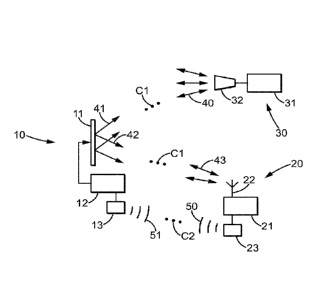
Figure 1 is a schematic view showing a cellular
communication network, which is known to comprise:
- a network station 30 responsible for transmitting
and receiving radio communications into a first
communication channel Cl (primary wave
propagation
channel), for example corresponding to a mobile phone
station, or an internet box diffusing internet inside a
building via WiFi, and
- an electronic device 20, for
example
corresponding to a mobile phone, a laptop computer equipped
with a mobile telephony module or WiFi module, or any
device equipped with such a mobile telephony or WiFi
module.
The electronic device 20 is mobile or movable from
one place to an other. It is powered via an electric plug
or powered via an internal battery. The electronic
device 20 may not be mobile, and the location of the
electronic device 20 may be determined by various reasons
that do take care of the quality of radio reception from
the network station 30.
According to the invention, this communication
network further comprises a shaping device 10 placed at a
CA 02924134 2016-03-11
WO 2015/039769
PCT/EP2014/056568
11
short distance or at short range from the movable
electronic device 20. The aim of this shaping device 10 is,
for example, to improve the reception of the electronic
device 20 in an area encompassing the electronic device and
in the vicinity of the shaping device 10. This shaping
device 10 is, for example, useful in an environment causing
many and/or complex reflections of electromagnetic waves,
where these reflections interfere with the reception of the
electronic device 20. The shaping device 10 generates
another reflection and/or a transmission which is
controlled for example in order to improve the reception of
the electronic device 20.
The network station 30 for mobile telephony
comprises:
- a communication unit 31 that receives a
communication to be transmitted to an electronic device 20
(mobile phone),
- a network antenna 32 which transmits the
communication by a transmission radio wave 40 which
propagates into the first communication channel Cl.
The first communication channel Cl is a
communication channel suitable for mobile telephony, for
example such as GSM or UMTS, or suitable for a computer
network, for example such as WiFi, Bluetooth, or NFC.
The electronic device 20 comprises at least:
- an antenna 22 (or receiving device) for receiving
and transmitting a radio wave 43 in the first communication
channel Cl, and
- a processing unit 21 connected to
said
antenna 22, for processing signals from and to the
antenna 22.
The electronic device 20 normally receives a radio
wave (not shown) from the network antenna 32, either
directly or indirectly by reflection on environmental
elements. In the context of the present invention, it also
receives a modified radio wave 43 originating from a
CA 02924134 2016-03-11
WO 2015/039769 PCT/EP2014/056568
12
(reflected or transmitted) modified wave 42 originating
from the shaping device 10.
Advantageously, the
electronic device 20 also
comprises a transmission unit 23 for wireless communication
via a second communication channel C2.
The shaping device 10 comprises
- an (electromagnetic) surface 11 which reflects
and/or transmits an incident radio wave 41 as a (reflected
or transmitted) modified wave 42, said waves propagating
into the first communication channel Cl, and
- a controller 12 connected to the electromagnetic
surface 11 in order to control said electromagnetic
surface 11, in particular in order to vary an
electromagnetic impedance, thereby changing how the
incident wave 41 is reflected and/or transmitted as a
modified wave 42.
This shaping device 10 is advantageously located at
a location with difficult reception for electronic
devices 20. It is therefore at a short distance from the
electronic device 20. It reflects and/or transmits an
incident wave 41 emitted by the network station 30 or
reflected by another element of the environment or by
another shaping device. In a very simplified manner, the
modified wave 42 then propagates into the first
communication channel Cl as well, for example toward the
electronic device 20 (mobile device).
The U.S. patent no. 6538621 shows one type of
electromagnetic surface whose impedance is adaptable or
modifiable that can be used in the shaping device according
to the invention. This electromagnetic surface comprises a
plurality of resonant elements, each resonant element being
tunable. The electromagnetic surface of that patent
comprises array elements located at a distance from a
ground plane, adjacent array elements being connected
together by a variable capacitor arrangement, each variable
CA 02924134 2016-03-11
WO 2015/039769 PCT/EP2014/056568
13
capacitor controllable by a control potential. The
impedance of the electromagnetic surface is modified
accordingly, for example in order to focus the modified
wave or to give a direction to the modified wave.
Optionally, the electromagnetic surface 11 of the
invention consists of a plurality of cells (tunable
elements represented on figure 6), each cell comprising two
separate resonator elements. The first resonator resonates
at a first frequency fi and the second resonator resonates
at a second frequency f2 which is different from the first
frequency, said second frequency f2 also being tunable by a
variable capacitor or by a variable diode. Such a cell
allows reflecting an incident wave 41 with a positive sign
or a negative sign, depending on whether the second
frequency f2 is close to or far from the first frequencyfi.
The set of cells of the electromagnetic surface 11 allow
obtaining highly effective modifications to the impedance
of said surface.
Optionally, the set of cells (tunable elements 14)
of the electromagnetic surface 11 of the invention has a
single polarization type or two polarization types. In the
second case, the electromagnetic surface 11 comprises
resonator elements of the first and second polarization
types. The resonator elements of each type are
advantageously distributed over the entire surface, for
example in alternation. The electromagnetic surface 11 then
provides control of an incident wave 41, regardless of its
polarization type.
Optionally, the set of resonator or tunable
elements of the electromagnetic surface 11 has a single
resonance frequency or two or a plurality of resonance
frequencies. The electromagnetic surface 11 then allows
controlling a frequency range or band, or a plurality of
frequency bands depending on the proximity of the
frequencies in the plurality. The electromagnetic
surface 11 then allows controlling an incident wave 41 over
CA 02924134 2016-03-11
WO 2015/039769 PCT/EP2014/056568
14
a predetermined frequency band, which may be a wide
frequency band if the set of resonator elements covers this
frequency band.
The set of tunable elements may comprise only two
different states. The tunable element 14 is therefore a
binary element. All the tunable elements states define
specific impedance for the electromagnetic surface 11. The
two states may be a phase shift of modified wave regards to
the incident wave, or may be an amplitude shift of modified
wave regards to the incident wave. Thanks to these only two
states of each resonator tunable elements 14, the number of
combinations is reduced, but enough for optimization
process.
In case of phase shifts, each tunable element 14
may reflect or transmit the incident wave into a modified
wave having a phase shift relative to the incident wave,
said phase shift being preferably of zero radian for the
first state (meaning that the modified wave do not have is
phase modified) and Tc radians for the second state (meaning
that the modified wave has his phase shifted of Tc radian,
i.e. is the opposite wave).
Alternatively, the phase shift is of alpha radians
for the first state (alpha being an angle value between
zero and 'it) and alpha+Tc radians for the second state.
In case of amplitude shift, each tunable element 14
may reflect or transmit the incident wave into a modified
wave having an amplitude shift relative to the incident
wave (amplification coefficient), said amplitude shift
being preferably of zero for the first state (meaning that
the modified wave is null) and one for the second state
(meaning that the modified wave is identical to the
incident wave).
Additionally, more than two states can also be used
for having more flexibility.
The controller 12 of the shaping
device 10
CA 02924134 2016-03-11
WO 2015/039769 PCT/EP2014/056568
according to the invention controls, for example, all the
tunable elements (variable capacitors or diodes) of the
electromagnetic surface 11, thereby modifying the impedance
of the tunable element itself, and modifying the impedance
5 of the surface 11. This modification is much more complex
than focusing or spatial directivity. It alters the spatial
distribution of the radio wave into the first communication
channel Cl inside an area around the shaping device 10.
According to the invention, the shaping device 10
10 comprises a transmission module 13 connected to the
controller 12. This transmission module 13 is essentially a
means for receiving a wave (a receiving device) and
converting it into a pilot signal. This pilot signal is
either representing the wave (main or primary wave)
15 propagating into the first communication channel Cl, or an
other wave propagating into a second communication
channel C2 (that is different from the first communication
channel). In some cases, the transmission module 13 may
optionally send information to an electronic device 20.
In the first case, the transmission module 13 is a
radio transmission antenna adapted for the first
communication channel Cl, for example a telephony channel.
In the second case, the transmission module 13 is a
transmission antenna for a second communication channel C2
which is advantageously a channel for short-range
communications, e.g. a distance lower than 100 meters in an
unobstructed field. It experiences less or little
interference from environmental elements.
In a first variant, the transmission module 13 is
for example an electromagnetic antenna for wireless data
transmission, for example WiFi or Bluetooth, and the second
communication channel C2 is an electromagnetic channel.
In a second variant, the transmission module 13 is
for example an acoustic transducer, such as a speaker
and/or microphone or a combination thereof, and the second
communication channel C2 is acoustic. In this case, the
CA 02924134 2016-03-11
WO 2015/039769 PCT/EP2014/056568
16
second communication channel C2 is advantageously in an
inaudible frequency band, for example ultrasonic. Thus, the
mobile electronic device 20 can transmit data to the
shaping device 10 without this transmission of data being
perceptible to a user.
Other variations of the transmission module 13 are
possible. For example, the transmission module 13 is an
optical transducer (ultraviolet or laser).
The data transmitted in the second communication
channel C2 between the electronic device 20 and the shaping
device 10 can be of various types, depending on the
distribution of the software modules or functions between
the electronic device 20 and the shaping device 10.
The controller 12 modifies the tunable elements of
the electromagnetic surface 11 according to the pilot
signal received by the transmission module 13, thereby
modifying the impedance of the surface 11.
By means of the pilot signal, the controller 12
orders modifications to the impedance of the
electromagnetic surface 11 based on information on the wave
received either directly by the shaping device 10
(autonomous operation) or via an electronic device 20
(controlled operation). As the electronic device 20 is at
short-range from the shaping device 10, the controller 12
modifies the impedance of the surface 11 based on
information on the wave received at a location near the
shaping device 10. The modification of the wave received by
an electronic device 20 in proximity to or at short-range
from the shaping device 10 can therefore be better tuned or
adapted than any modification to the wave emitted by the
network station 30. In this manner, the shaping device 10
does not have a wired connection to the network station 30,
and is not controlled by the network station 30. In other
words, the shaping device 10 therefore has no information
on the wave source (electromagnetic, acoustic or
vibrational).
CA 02924134 2016-03-11
WO 2015/039769 PCT/EP2014/056568
17
According to a first embodiment of the invention,
represented in figure 2, the electronic device 20 comprises
a monitoring unit 21a that determines at least one value
corresponding either to:
- a strength of the signal received by the
antenna 22 (power level or amplitude of the radio signal
received over a predetermined period of time), or to
- a quality index for the radio wave received (for
example communication error rate into the first
communication channel).
The electronic device 20 then transmits this value
to the shaping device 10 by a transmission unit 23 of the
same type as the transmission module 13 of the shaping
device 10 (compatible). This value may be included into a
set of data transmitted by the transmission unit 23 of the
electronic device 20 to the transmission module 13 of the
shaping device 10. The
transmission unit 23 of the
electronic device 20 thus emits a wave 50, which propagates
into a second communication channel C2 towards the shaping
device 10, in a wave 51 representing or also called the
"pilot signal". In this case, the second communication
channel C2 is different from the first communication
channel Cl. This second channel C2 has less interference
than the first one, and the shaping device 10 is easily
connected to the electronic device 20 in order to modify
the impedance of the electromagnetic surface 11.
The shaping device 10 receives the value by its
transmission module 13, which provides it to the
controller 12.
The controller 12 of the shaping device 10
comprises:
- an optimization module 12b which receives said
value from the transmission module 13 and determines
control parameters for the electromagnetic surface 11, and
- a control module 12a connected to
the
CA 02924134 2016-03-11
WO 2015/039769 PCT/EP2014/056568
18
electromagnetic surface 11, said control
module 12a
applying the control parameters to the electromagnetic
surface 11 in order to modify its impedance.
The optimization module 12b executes an
optimization algorithm based on the set of (temporally)
previous parameters, previous values, and the current value
provided by the electronic device 20.
The optimization algorithm may be a maximization or
minimization of the value. For example, if the desired goal
is to increase the intensity of the signal received by the
electronic device 20, the optimization algorithm will look
for a maximum. Conversely, if the desired goal is to reduce
the intensity of the signal received by the electronic
device 20, the optimization algorithm will look for a
minimum. In several successive steps, the optimization
algorithm provides an optimum set of parameters.
The control unit 12a of the controller 12 then
applies the set of parameters determined by the
optimization module 12b and controls the tunable resonator
elements of the electromagnetic surface 11. This determines
a particular state of the electromagnetic surface 11, which
modifies the radio wave 42 reflected or transmitted by said
electromagnetic surface 11.
The radio wave 43 received by the electronic
device 20 is a combination of this reflected and/or
transmitted modified radio wave 42 and a radio wave from
the network antenna 32. The state of the electromagnetic
surface 11 thus modifies the reception of the radio wave 43
received by the electronic device 20.
In several successive steps, during which the
control parameters for the electromagnetic surface 11 are
applied by the controller 12 and values are obtained by the
monitoring unit 21a of the electronic device 20, the
algorithm of the optimization module 12b implemented in the
controller 12 finds a set of optimum control parameters
corresponding to the desired goal (optimization criterion).
CA 02924134 2016-03-11
WO 2015/039769 PCT/EP2014/056568
19
There are numerous known optimization algorithms
that may be used: LMS (least mean squares), genetic,
simplex, etc.
Optionally, once the optimization is done, the
shaping device 10 can
transmit information to the
electronic device, via the
transmission module 13,
concerning the optimization performed, its status, and its
performance.
The electronic device 20 is independent from the
shaping device 10: it can communicate by the first
communication channel Cl even before the process of
optimizing the impedance of the electromagnetic surface 11
is carried out or completed.
According to a second embodiment of the invention,
represented in figure 3, the electronic device
20
comprises:
- a monitoring unit 21a connected to
the
transmission unit 23, and being similar or identical to the
one in the first embodiment, and
- an optimization unit 21b that is equivalent to
the optimization module 12b of first embodiment.
This optimization unit 21b is now implemented
inside the electronic device 20, and the latter transmits
the set of parameters to the shaping device 10 via the
transmission unit 23. The set of parameters can be included
into a set of data transmitted by the transmission unit 23
of the electronic device 20 to the transmission module 13
of the shaping device 10. The transmission unit 23 of the
electronic device 20 thus emits a wave 50, which propagates
into a second communication channel C2 to the shaping
device 10 in a pilot signal 51. The second communication
channel C2 is different from the first communication
channel Cl, with less interference, and the electronic
device 20 easily connects to the shaping device 10 in order
to modify the impedance of the electromagnetic surface 11.
The shaping device 10 receives the set
of
CA 02924134 2016-03-11
WO 2015/039769 PCT/EP2014/056568
parameters via its transmission module 13, and
the
controller 12 which comprises only the control module 12a
applies this set of control parameters to the
electromagnetic surface 11 in
order to change its
5 impedance.
The shaping device 10 of the second embodiment is
then working as the one the first embodiment.
In the third embodiment, illustrated in figure 4,
10 the shaping device 10 is autonomous and comprises a
transmission module 13 that is for example a microphone.
The shaping device 10 comprises:
- a monitoring module 12c
connected to the
transmission module 13, said monitoring module 12c being
15 equivalent (similar or identical) to the monitoring
unit 21a implemented inside the electronic device in the
first and second embodiments,
- an optimization module 12b which receives the
value from the monitoring module 12c and determines control
20 parameters, and
- a control module 12a connected
to the
electromagnetic surface 11, said control
module 12a
applying the control parameters to the electromagnetic
surface 11 in order to modify its impedance.
The optimization module 12b integrated into the
controller 12 of the shaping device 10 minimizes or
maximizes a value, such as the level of reception of the
acoustic wave 51 received by the microphone 13 and
originating from an unknown sound source. The shaping
device 10 of this third embodiment is then autonomous.
The shaping device 10 of the third embodiment is
then working as one of the previous embodiments.
The shaping device 10 is a controllable passive
device that consumes very little energy. It is not able to
emit itself an acoustic wave, without an incident acoustic
wave 41.
CA 02924134 2016-03-11
WO 2015/039769 PCT/EP2014/056568
21
In all embodiments of the invention, the shaping
device 10 is a device independent from the network
station 30 and its antenna. The shaping device 10 is
autonomous, and responds to an electronic device 20 in
order to optimize (maximize or minimize) the reception of
said electronic device 20.
The shaping device 10 may take the form of a panel,
for example mounted on a wall of a space, room, house, or
area to be controlled.
An electronic device 20 which lies within the scope
of this shaping device 10, and which comprises for example
a software module for connecting via its transmission
unit 23 to said shaping device 10, may automatically
request modifications to the impedance of the
electromagnetic surface 11 of the shaping device 10.
The electronic device 20 may optionally connect to
multiple shaping devices 10 to provide better control of a
specific spatial area.
The shaping device 10 may optionally connect to
multiple electronic devices 20 in order to modify the
impedance of the electromagnetic surface 11 according to
the multiple objectives of each electronic device. For
example, it is possible to modify the impedance of the
electromagnetic surface 11 to enhance or increase the
reception on two electronic devices 20. It is also possible
to modify the impedance of the electromagnetic surface 11
in order to increase reception into a first spatial area
around a first electronic device, and simultaneously cancel
out or reduce the reception into a second spatial area
around a second electronic device.
In the first embodiment, each shaping device 10
will optimize its set of parameters. All the shaping
devices 10 are advantageously identical, and the electronic
device 20 is doing very little processing and computing.
In the second embodiment, the electronic device 20
CA 02924134 2016-03-11
WO 2015/039769 PCT/EP2014/056568
22
can determine the sets of parameters for each shaping
device 10 while taking into account combinations, which can
provide better electromagnetic processing and better
control for the area. All the shaping devices 10 are
simplified and preferably identical. However, the
electronic device 20 will perform more calculations and
more processing to determine the sets of parameters for all
the shaping devices 10.
It should be noted that the electromagnetic
surface 11 is a passive device that consumes very little
power. This device does not emit additional electromagnetic
radiation. It modifies the local electromagnetic field by
moving the nodes (minima) and antinodes (maxima) of the
electromagnetic field. This device is therefore not an
amplifier or repeater of a wave. Its energy consumption is
mainly due to the controller 12 and its short-range
transmission module 13.
The shaping device 10 may therefore be an
autonomous device, where appropriate powered by a
rechargeable battery.
The shaping device 10 may also comprise a power
supply component that may be connected to the
electromagnetic surface 11 for recovering an amount of
energy from the incident wave. The amount of energy
recovered is enough for powering the shaping device 10.
The shaping device 10 may also comprise a power
supply component that may be connected to a photoelectric
cell for recovering an amount of energy for example from
the sun light or ambient light.
Additionally, the shaping device 10 may comprise
means for providing energy to the electronic device 20. For
example, the shaping device 10 incorporates a connector for
connecting the electronic device 20 and for refilling its
battery.
It should also be noted that the location of the
shaping device 10 within the processing area is important
CA 02924134 2016-03-11
WO 2015/039769 PCT/EP2014/056568
23
to its effectiveness. A prior step of determining this
location is therefore preferred. The shaping device 10
and/or the electronic device 20 may include a software
module for determining said location.
In addition, the transmission module 13 may consist
of a single transducer or a plurality of transducers
distributed spatially. In the case of the third application
(jamming an interfering transmitter), these transducers
will be distributed so as to cancel out far-field emissions
of such an interfering transmitter. Furthermore, the
transducer or transducers of the transmission module 13 may
be integrated and/or distributed on the electromagnetic
surface 11 in order to form a single integrated device.
Finally, in the case of a shaping device 10 which
comprises a broadband electromagnetic surface 11 (for
example with resonator elements at multiple resonance
frequencies), the optimization modules 12b, 21b can perform
optimization:
- either for each frequency independently of an other
frequency (in this case, each frequency of the reflected
wave may have any phase);
- or for all frequencies considered synchronously. In this
case, each frequency of the (reflected and/or transmitted)
modified wave can have a predetermined phase relative to an
other frequency. It is then possible to readjust the phase
of all frequencies relative to each other in order to carry
out broadband focusing.
Additionally, in the various embodiments, the
electronic device 20 may be composed of two parts: a first
one having a first casing incorporating at least the
processing unit 21 and a second one having a second casing
incorporating at least the transmission unit 23.
The first and second casing being removably
attached one to the other for connecting the processing
unit 21 to the transmission unit 23. The casings may
comprise complementary shapes for attachment, and for
CA 02924134 2016-03-11
WO 2015/039769 PCT/EP2014/056568
24
example elastic clips.
The processing unit 21 is connected to the
transmission unit 23 via a wired or wireless connection.
They are for example connected together via a USE port.
Thanks to these features, the first part may be a
conventional mobile phone, and the second part may add to
the mobile phone hardware and software capabilities so that
to be able to control a shaping device 10.
The shaping device 10 according to the invention
has many possible uses: improving mobile phone reception in
an area where there are interferences, canceling out mobile
phone reception in a specific area where they are
prohibited or in order to protect from radio waves,
canceling out reception of wireless transmissions such as
WiFi within a specific area.
For example, it is possible to place the electronic
device 20 above a baby's crib and the shaping device 10
inside the baby's room. The electronic device 20 controls
the shaping device 10 in order to cancel out any radio
waves (of cellular phones or WiFi) at the crib, without
canceling out said waves throughout the entire house.
Finally, the optimization module is a software
module that can be implemented, added, and updated easily
within the electronic device 20 or the shaping device 10.
In particular, this optimization module can be downloaded
easily via the network of the first communication
channel Cl or via the network of the second communications
channel C2.
The various embodiments of the invention may also
be applied to the field of acoustics, in which the primary
wave (source) is an acoustic wave.
The shaping device 10 then comprises a plurality of
acoustic resonator elements having a tunable portion for
modifying its impedance. These resonator elements are, for
CA 02924134 2016-03-11
WO 2015/039769 PCT/EP2014/056568
example, Helmholtz resonators comprising a cavity and a
tube connecting the cavity to the outside. For example, the
cavity or tube has a tunable dimensional characteristic.
The resonator element may also be an electromagnetic
5 actuator moving a membrane and having a moving mass. It may
also use an active membrane, such as an electroactive
polymer membrane
This acoustic shaping device 10 is able to reflect
and/or to transmit an incident acoustic wave 41 as a
10 modified acoustic wave 42. The first propagation channel Cl
is then an acoustic channel.
The shaping device 10 further comprises a
controller 12 of the same type as those already described.
In the first and second embodiments of figures 2
15 and 3, the shaping device 10 has a wireless connection with
an electronic device 20 in order to pilot modifications to
the acoustic impedance of the shaping device 10 as a
function of the wave 43 received by the receiving unit 22
(microphone) of the electronic device 20.
20 The optimization module 12b integrated into the
controller 12 or the optimization module 12b integrated
into the electronic device 20 allows minimizing or
maximizing, for example the level of reception of the
received acoustic wave 43.
Finally, the
shaping device 10 or only the
surface 11 may be directly integrated into a constructional
element of a building: a concrete block, a brick,
insulation, an insulating board, a plasterboard, or any
other element.
The shaping device 10 or only the surface 11 may be
directly integrated into decorative elements of a building:
wood flooring, carpeting, tile flooring, a trim panel, a
partition, a ceiling, a dropped-ceiling panel, or other
element.
The shaping device 10 or only the surface 11 may be
CA 02924134 2016-03-11
WO 2015/039769 PCT/EP2014/056568
26
directly integrated into furnishings: a desk, cabinet,
bookcase, mirror, decorative table, and lamp.
This element comprises at least the surface 11 of
the shaping device or the entire shaping device 10. It may
be powered externally, or comprises a battery, or can be
remotely powered by induction which is possibly continuous.
Experimental results
An electromagnetic surface 11 (also called tunable
metasurface) is experimentally tested. The optimization
method of a shaping device 10 or electronic device 20 or
system according to the invention is also tested in the
following. The surface 11 is created and covers one small
part of the walls of a typical office room as illustrated
on figure 5.
The electromagnetic surface 11 is for example
composed of two panels 11a, 11b, each comprising an array
or grid of tunable resonant elements (also called unit
cells).
Each tunable resonant element 14 is for example a
planar resonator as represented on figure 6 and is able to
reflect the waves with a controllable phase shift. We
choose to work with resonators that sit on a ground plane
since they will anyway be placed on walls, which are ground
planes albeit poor ones. For the sake of simplicity and
rapid convergence of the optimizations, we opt for the
simplest case of a binary phase modulation, that is, a two
states resonator that reflects the waves either positively
or negatively; it is similar to the binary amplitude
modulation realized in optics. To do so, a choice is a
resonator that presents a resonance frequency fief which can
be shifted using an electronic circuit. If the resonance
frequency fief is set such that it corresponds to the working
frequency fo, the resonator reflects the waves at this
frequency with a Tc phase shift. Now when its resonance
frequency is shifted away from fo, the resonator is
CA 02924134 2016-03-11
WO 2015/039769 PCT/EP2014/056568
27
transparent and the ground plane reflects the waves with a
0 phase shift.
We opt for a slightly more complicated design which
consists in two strongly coupled or hybridized resonators
as described in figure 6. The first resonator 14a is called
reflecting resonator and is polarized along its short axis
which resonance frequency fief is set to the working
frequency fo, while the second resonator 14b is a parasitic
strip resonator whose resonance frequency fpõ can be
electronically tuned from the working frequency fo to a
higher frequency fi using a diode 14c. Doing so, when the
resonance frequency fpõ is set to the higher frequencyfi,
the reflector resonance frequency fief is unchanged and it
reflects the waves with a Tc phase shift ('it-state). On the
contrary when the resonance frequency fpõ is shifted to the
working frequencyfo, the two resonators hybridize and a
dimmer presenting two resonant frequencies f- and f+ around
fo is created. In this state, at the working frequency fo,
the dimer is again transparent and the waves are reflected
by the ground plane with a 0 phase shift (0-state).
This design presents notable advantages: the
reflection properties of the resonant element 14 are
insensitive to both the losses and impedance variations of
the electronic components and to the soldering which are
placed on the parasitic resonator only.
The electromagnetic surface 11 is
a spatial
microwave modulator SMM, having an area of approximately
0.4 m2 comprising 102 tunable resonant elements, spaced by
half a wavelength at the working frequency fo=2.47 GT1z, that
is, 6 cm. This tunable metasurface, which is 1.5 mm thin,
is a kind of smart wall.
The experimental setup of the office room is
schemed in figure 5. We control the 102 resonant elements
using two Arduino controllers, each having 54 channels of
digital outputs. An Agilent network analyzer is used to
measure the transmission between a source antenna S and a
CA 02924134 2016-03-11
WO 2015/039769 PCT/EP2014/056568
28
receiver antenna R. The receiver antenna R is a regular
monopole antenna or an electro-optic probe when spatial
scanning is realized. We use commercial monopole Wi-Fi
antennas polarized along the same axis than the resonant
elements 14 of the electromagnetic surface 11. The source
antenna S is placed far away and out of sight of both
receiver antenna R and the electromagnetic surface 11,
inside a furnished and hence scattering 3x3x4 m3 office
room (figure 5), thereby creating in the whole room and
notably on the smart walls a random microwave wave field.
The receiver antenna R is placed for example one meter away
from the electromagnetic surface 11.
We first characterize the
electromagnetic
surface 11. To do so, we measure the resonance frequency of
each resonant element 14 of the array in the 0 and Tc
states, using near field probes. The resonance frequencies
histogram shows that the 'it-state distribution is relatively
narrow and centered on the working frequency fo, while the
0-state distribution is somewhat broader due to the
electronic components but still not overlapping the 'it-state
one.
We also evaluate the bandwidth (see figure 7) of
the electromagnetic surface 11 by displaying 11000 random
configurations (out of 2102 combinations of the 102 resonant
elements of the electromagnetic surface array) and
measuring the standard deviation of the transmission
between the source antenna S and the receiver antenna R. We
do so for 10 different positions of the source antenna S to
average over disorder. This smoothes the spectral
variations of the transmission that are due to the room and
this gives an estimate of the efficiency of the
electromagnetic surface 11 as a function of frequency. We
measure a bandwidth of around 100 MHz which can be
attributed to the bandwidth of each resonant element and
their dimension distribution due to fabrication
uncertainties.
CA 02924134 2016-03-11
WO 2015/039769 PCT/EP2014/056568
29
In the experiments, we use this SMM to optimize the
multiply scattered waves existing in the office room and
recycle them for various purposes. For the sake of
experimental simplicity the source of microwaves is the
network analyzer connected to source antenna S. It results
in a random wave field similar to the one that would be
created by any remote wireless source such as a base
station or a Wi-Fi box. Furthermore since the feedback used
is not coherent, optimizing this electromagnetic field or
any other one is strictly equivalent.
1) Use to improve wireless signal reception:
We now use an intensity feedback mechanism to
passively optimize the reflection of the multiply scattered
waves off the electromagnetic surface 11 such that they
focus on the receiver antenna R. Namely, we start with a
uniformly reflecting electromagnetic surface 11 (all pixels
in 0-state). Then, we iteratively switch each pixel of the
array to the it-state and we measure for each one the
intensity received on receiver antenna R using the network
analyzer. This energy feedback is provided by the computer
to the electromagnetic surface 11, that is, if the received
energy is higher, the pixel is kept on the it-state,
otherwise it is switched back to the 0-state. In a real
application scenario, the receiver antenna R could be a
smart phone that uses an application which measures in real
time the binary error rate of an ongoing communication, and
sends a binary feedback based on this estimation to the
electromagnetic surface 11, for instance using low
frequency ultrasounds. We perform 30 optimizations to
average over disorder. For each one we scan the microwave
field before and after optimization using a non
perturbative electro-optic probe.
Figure 8 displays the efficiency 1 of the intensity
obtained using the optimization, defined as the ratio
between intensities measured after and before maximization.
CA 02924134 2016-03-11
WO 2015/039769 PCT/EP2014/056568
Figure 9 shows the corresponding intensity spectra of the
transmission between the source antenna S and the receiver
antenna R before the maximization (continuous line) and
after the maximization (dotted line). The maps of the field
5 intensity around the receiver antenna R positioned at the
point coordinates (0,0) is
shown on figure 9 before
maximization and on figure 10 after maximization. Clearly,
even though the source antenna S is out of sight of both
the receiver antenna R and the electromagnetic surface 11,
10 the electromagnetic surface 11 can passively focus the
multiply scattered waves onto the receiver antenna R on a
half wavelength wide focal spot. This literally turns the
random wave field into a focused one, thereby providing a
net gain of 8.5 dB on the receiver antenna R, almost a
15 decade. The corresponding spectra corroborates this
conclusion, and indicates that the effect survives over a
bandwidth of approximately 30 MHz, limited by the
correlation frequency of the office room. The inset of
figure 8 presents the phase mask obtained at the end of the
20 optimization. A black square in the array shows a Ophase
state of the resonant element and a white square in the
array shows a p-phase state of the resonant element. This
again proves that the field on the electromagnetic
surface 11 is random.
25 The above experiments were also done for the 30
realizations of disorder. The data are normalized by the
measured mean intensity before optimization. It shows that
the average efficiency 1 obtained is around 8.5 dB, with a
minimum of 5 dB, for an intensity which was relatively high
30 before optimization, and a maximum of 35 dB, more than
three orders of magnitude, for a very low initial
intensity. Spatially, on average, the field is tightly
focused around the receiver antenna R, again on a focal
spot half a wavelength wide. The mean intensity spectrum,
which is almost flat before optimization, meaning that
the 30 realizations have almost erased the effect of
CA 02924134 2016-03-11
WO 2015/039769 PCT/EP2014/056568
31
scattering and reverberation, clearly displays a peak
at 2.47 GHz after maximization, as a signature of the
focusing effect.
We have also performed experiments with both
receiver antenna R and source antenna S out of sight of
each other and the electromagnetic surface 11, the three
part being spaced one from another by about 3 meters. The
results prove that even in this worst case scenario
efficiency 1 between 1.5 dB and 6 dB are realizable, with
an average of 2.5 dB. It is worth noting that the
electromagnetic surface 11 used is only an area of 0.4 m2
as compared to the total wall area of the 3x3x4 m3 office
room. Using larger SMMs
(electromagnetic surface 11)
increases drastically the performances of the approach.
2) Use to protect volumes from the penetration of
microwaves:
We now use the intensity feedback to cancel the
electromagnetic field in a given volume thanks to
interferences.
To demonstrate this, we use the same optimization
procedure than before, albeit with an energy minimization
goal. The reception is minimized on receiver antenna R
which is again placed at position (0,0), and an electro-
optic probe is used to scan the field before and after the
minimization without perturbing it. We
perform 30 measurements in order to average over disorder
and, again, the energy feedback is transmitted by the
computer to the electromagnetic surface 11 during the
procedures. In a practical application, a passive microwave
receiver could be used to measure the electromagnetic
energy on a set of sensors and send the feedback to the
electromagnetic surface 11, in order for instance to
protect a given volume from penetration of Wi-Fi microwave.
Likewise for the maximization, the results of a
single realization of minimization are presented on
CA 02924134 2016-03-11
WO 2015/039769 PCT/EP2014/056568
32
figures 12-15, including the measured intensity spectra and
maps before and after the minimization, as well as the
diminution of the efficiency i (ratio of intensity before
and after minimization) as a function of the iteration
number. It proves that an optimized random phase mask
permits, as opposed to the bare wall, to decrease the
electric field on the receiver antenna R by about 25 dB.
The spatial scans and intensity spectra further confirm
that the field has been cancelled locally around 2.47 GHz.
The results of 30 realizations of disorder are
shows that the averaging has been correctly performed since
the average field intensity is almost constant on the
initial spatial scan, and the averaged initial spectrum
almost flat on the considered bandwidth. The
30 measurements prove that the field can indeed be
cancelled at the desired location around the working
frequency fo, onto a volume of about half a wavelength cube,
down to a level which is here limited to our measurement
noise to about -28 dB. Evidently, higher
initial
intensities lead to better efficiency 1 of about 35 dB,
while lower initial intensities amount lead to about 20 dB
intensity drops, all realizations converging towards the
experimental noise level.
Theoretical analysis
After these experiments, it is necessary to
evaluate quantitatively the possible benefits that can
bring the approach in terms of energy saving for wireless
communications or in terms of electromagnetic protection.
To start with, the method used amounts to wavefront shaping
inside reverberating media and using an electromagnetic
surface 11. A typical indoor room is a cavity for
electromagnetic waves, albeit a leaky one. Quantifying the
outcome of the smart walls consists in estimating the
number n of spatial modes that are controlled with the
electromagnetic surface 11 versus the total number of
CA 02924134 2016-03-11
WO 2015/039769 PCT/EP2014/056568
33
spatial modes N that participate to the wavefield in the
given room at the working frequency fo. This allows us to
calculate the average efficiency or intensity drop
factors i which can be achieved for a given electromagnetic
surface 11 in a given room.
In the model for the sake of simplicity the field
is scalar, the resonant element 14 belonging to the
electromagnetic surface 11 reflects the
waves
isotropically, and a room is approximated by a cuboid
cavity of volume V with part of its walls covered by an
electromagnetic surface 11 of area S. We consider a regular
cavity although rooms can be irregular and are typically
furnished hence disordered, but the latter will only serve
us to calculate the modal density, which is equal on
average for regular and random cavities. A cavity can be
described by two characteristic times. The first one, the
reverberation time TR, represents the average time a photon
spends in the cavity: it is formally equivalent to the
Thouless time in disordered media. The second one, the
Heisenberg time TH, represents the time a photon would need
to propagate inside the cavity in order to resolve all of
its discrete eigenmodes. The inverse of the reverberation
time is the correlation frequency
,,00r of the medium:
fcorr = ¨
TR .
The correlation frequencyfoor corresponds to the
frequency bandwidth over which the modes of the cavity are
spectrally coherent. In order to estimate the total number
of spatial modes N, we must quantify the number of
eigenmodes of the cavity that overlap over one frequency
correlation of the cavity. This number is approximately
given by the Heisenberg time, which equals the modal
density of the cavity, multiplied by the correlation
frequency of the medium:
N = T fcorr
For a cuboid of volume V, at the working
CA 02924134 2016-03-11
WO 2015/039769 PCT/EP2014/056568
34
frequencyfo, and with c the speed of light, it is:
_8Thvfo2fc0rr
N T 11 fcorr
As for the number n of modes controlled by the
electromagnetic surface 11, it is given by the ratio
between its area and the correlation area of the field in
the room, which equals the resonant element 14 area in our
case:
4S
n ,=--
A2
When the electromagnetic surface 11 is not
optimized, it behaves just as a regular wall. At any
position in the room the field is an incoherent sum of
the N spatial modes: the variance of its norm hence scales
as a random walk: N. Optimization aim at adding in phase
the n modes controlled with the electromagnetic surface 11
in order to maximize the field or push its norm towards
zero. The field after optimization is the incoherent sum of
the uncontrolled N¨n modes plus or minus the coherent sum
of the n controlled modes. We can hence write the
efficiency or intensity drop factors brought by the
electromagnetic surface 11 as:
(-
+
n+A/Til2
n =
where
+ corresponds to maximization of the field with
n < N, and
the condition
- represents the minimization which is only
valid for n \/N-n
This finally allows us to quantify the efficiency
and intensity drop factors as a function of the parameters
of the smart walls and room, at the working frequency:
(, 1 2s2fd .\11 Sc
TCCI Ucorr 27EV fcorr)2
which can be approximated to
-= 1 + _____________ 2S2)
Trtvicorr if n << N
CA 02924134 2016-03-11
WO 2015/039769 PCT/EP2014/056568
The above equation gives the average gain obtained
using smart walls in a room, or the area of the
electromagnetic surface 11 required for improving or
5 canceling locally the electromagnetic field.
Figures 16 and 17 show the efficiency (improvement
and intensity drop) as a function of the room volume V and
the electromagnetic surface area S for a correlation
frequency of 30 MHz as estimated experimentally and our
10 working frequency fo of 2.47 GHz. On figure 16, an average
a 20 dB gain over the wireless reception is obtained with
a 2.5 m2 electromagnetic surface 11 in a room having a
volume of 40 m3. In this configuration the system could
permit to decrease the power emitted by wireless sources,
15 whether base stations or a Wi-Fi boxes, by a factor of 100
without damaging the quality of the reception. On
figure 17, the electromagnetic field on given locations was
cancelled using a small electromagnetic surface 11. For
instance an electromagnetic surface 11 having an area
20 of 0.3 m2 cancels entirely the field at any location in a
room having a volume of 40 m3. Of course, protecting larger
volume from the penetration of microwaves requires larger
smart walls. Finally, using this model and correcting for
the binary only phase modulation, we find an average gain
25 of 4.9 dB for the fabricated electromagnetic surface
of 0.4 m2 that was used in the 3x3x4 m3 office room of the
experiments, right in between the average best and worst
case measured, and a minimum of electromagnetic surface
area of 0.45 m2 necessary to cancel the field locally, in
30 accord with our experiments. This tends to prove that the
model, accurately predicts the performances of our
approach.