Note: Descriptions are shown in the official language in which they were submitted.
CA 02924160 2016-03-18
APPLICATION FOR PROVISIONAL PATENT
for
MASKLESS PATTERNING
CA 02924160 2016-03-18
MASKLESS PATTERNING
FIELD OF THE INVENTION
[0001] The present invention relates to the fabrication and patterning of
different layers
for forming interconnects, devices, or other form of structure on a substrate.
BRIEF SUMMARY
[0002] one embodiment is a method of creating an array of vertical devices by
modifying
the lateral conduction without isolating the active layers
[0003] One embodiment is a method of transferring pattern to a photosensitive
material
which consists of Aligning a display to the substrate by using image sensor or
camera and
showing the intended pattern in the display.
[0004] Here, alignment procedure uses some physical alignment marks in the
display.
[0005] In another embodiment display shows alignment marks with light that is
not
reacting to the photosensitive materials for alignment procedure.
[0006] In one embodiment, intended pattern is modified to aligned with the
substrate
features and then showed in the display
[0007] In one embodiment, the display can be the same size as the substrate.
[0008] In another embodiment, the display sweeps the substrate or part of the
substrate
while the content of the display is scrolling to cover the intended pattern
for transfer
[0009] Here, the speed of scrolling and sweeping is controlled by the required
exposure
time
[0010] In one structure, the sensor pixels are distributed between the display
sensors.
[0011] In another structure, two separate display and image sensors are used.
BRIEF DESCRIPTION OF THE DRAWINGS
[0012] The foregoing and other advantages of the disclosure will become
apparent upon
reading the following detailed description and upon reference to the drawings.
[0013[ FIG. 1 shows a patterning system consists of display and imager.
[0014] FIG. 2 shows an embodiment for transferring a pattern to another medium
(e.g.
photoresist).
[0015] FIG. 3 shows another embodiment for transferring a pattern to another
medium
(e.g. photoresist).
CA 02924160 2016-03-18
[0016] FIG. 4 shows an embodiment of the pattern transfer system with separate
display
and imager (camera).
[0017] FIG. 5 shows an embodiment of the pattern transfer system with combined
display
and imager (camera).
[0018] While the present disclosure is susceptible to various modifications
and alternative
forms, specific embodiments or implementations have been shown by way of
example in the
drawings and will be described in detail herein. It should be understood,
however, that the
disclosure is not intended to be limited to the particular forms disclosed.
Rather, the disclosure
is to cover all modifications, equivalents, and alternatives falling within
the spirit and scope of
an invention as defined by the appended claims.
DETAILED DESCRIPTION
[0019] This document discloses various methods for using a display to transfer
a pattern to
a light sensitive medium. Here, the pattern is shown in a display creating
light in the operation
range of the light sensitive medium. After that the other processing steps
(such as backing,
developing, etching.....) to develop the pattern are followed up.
[0020] In this disclosure, display may include some optics or in some
embodiment separate
optic structure are listed. In this disclosure sensor array and camera are
used interchangeably.
The sensor can be a two dimensional array or one dimensional. Multiple sensor
(camera) may
be used in several different location to offer better and faster alignment.
The display can be a
two dimensional or one dimensional structure. It can be monocolor or multi
color display.
Multiple displays may be used to speed up the pattern transfer function.
[0021] Figure 1 describes a block diagram of a pattern transfer system 102
using display
system 104 as medium to create the pattern. Here, a display 106 and optics 108
can be two
separate parts or fully integrated. Also, an image sensor system 112 is used
to control the
alignment of the patterns with previous structures or patterns. Here, the
sensor system 112
consists of an actual image sensor array 114 and optics 116. The optics 116
can be part of the
sensor array 114 or separate structure. Also, one can share the display optics
108 and the
sensor optics 116 can be shared.
CA 02924160 2016-03-18
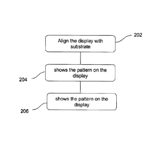
[0022] Figure 2 highlights operational steps for transferring the pattern to a
layer of
photosensitive material deposited on the substrate using a display. During
first step 202, the
display is aligned with the substrate, previous structures, or previous
patterns. In one case,
physical dimension of display is used as cue/mark for alignments. In another
case, a pattern is
shown in the display that is used as alignment mark. To avoid damaging the
photosensitive
material on the substrate, a different color (wavelength) can be used for
creating the alignment
marks on the display (e.g. red, yellow or other colors). The alignment
pattern/marks can be the
same as the actual pattern intended to be transferred to the photosensitive
layer. In another
case, physical alignment marks are added into the display structure. During
second step 204,
the intended pattern is created by the display. To properly transfer the
pattern to the
photosensitive material, it needs to be exposed to the pattern for a minimum
given time
(exposure time). Thus, the image needs to stay on the display for a given time
during third step
3, 206. These steps can be repeated to cover the entire substrate. Display can
move to new
location either as step function or sweeping function. In case of step
function, the display is
transferred to a new location while it is not showing a pattern that can
damage the
photosensitive layer. After the display is in the intended location, it shows
the adequate pattern
for transfer. In one case, locations may have some overlap. In case of
sweeping, as the display is
moving with a predefined speed, the pattern is scrolling to match the new
area. In this case, the
scrolling and sweeping speed can control the pattern exposure time or
combination of
scrolling/sweeping speed and wait step 206 can control the pattern exposure
time. One can
repeat alignment step 202 periodically to increase the speed.
[0023] In another embodiment, instead of physical alignment, the pattern on
the display is
modified to provide alignment with previous patterns. This structure, offer
faster alignment
with less complicated high accuracy physical moving parts. Figure 3 highlights
the main steps
for creating alignment using display picture. Here, the image sensor provide
an image of
previous pattern 302 (this can be the entire pattern, a part of it or just
alignment mark). In
addition, it may also include an image of the alignment in the display (either
its physical
dimension, alignment mark, pattern, or etc) in accordance with previous image.
During the next
step 304, the pattern image is modified to become aligned with the previous
pattern or
CA 02924160 2016-03-18
structure on the substrate. These steps 302, 304 can be repeated for offering
better alignment.
During third step 306, the modified pattern is created by the display. To
properly transfer the
pattern to the photosensitive material, it needs to be exposed to the pattern
for a minimum
given time (exposure time). Thus, the image needs to stay on the display for a
given time
during third step 4 308. These steps can be repeated to cover the entire
substrate. Display can
move to new location either as step function or sweeping function. In case of
step function, the
display is transferred to a new location while it is not showing a pattern
that can damage the
photosensitive layer. After the display is in the intended location, it shows
the adequate pattern
for transfer. In one case, locations may have some overlap. In case of
sweeping, as the display is
moving with a predefined speed, the pattern is scrolling to match the new
area. In this case, the
scrolling and sweeping speed can control the pattern exposure time or
combination of
scrolling/sweeping speed and wait step 308 can control the pattern exposure
time. One can
repeat alignment step 202 periodically to increase the speed.
[0024] Figure 4 highlights a system with two separate display 402 and image
sensor 403.
Here the display can cover the entire substrate 406 or just part of it. Also
multiple image
sensors 404 can be used. The display 402 shows the patterns either for
alignment or pattern
transfer. All the above procedure can be applied to this structure or all the
other structures
listed here.
[0025] Figure 5 shows a system with integrated image sensor into the display
502. Here
part of the display 502 can be the image sensor. In another structure, the
pixels for image
sensors can be distributed between the display pixels and so covering the same
area on the
substrate 506.
[0026] Figure 6 shows a system where image sensors 604 and display 602 are
connected
together and move together across the substrate 606.