Note: Descriptions are shown in the official language in which they were submitted.
1
APPARATUS AND METHOD FOR CONNECTING A CABLE TO A HIGH
TEMPERATURE CIRCUIT.
Technical field of the invention.
The invention relates to a device for connecting a cable to a circuit board at
temperatures
where conventional connection components based on polymers melt or soften to a
degree
that causes a malfunction.
io Background.
In general applies that it is beneficial for detecting instrumentation that
all or part of the
instrument is close to the phenomenon or medium where physical values are to
be
detected or measured. Common physical values or parameters are pressure,
temperature,
and dielectric constant. Deriving the medium which is present can in many
important
situations made from the dielectric constant. In a majority of processing
industries,
among these the petroleum industry, it is beneficial to be able to determine
the
relationship between water, oil and gas in a pipe or a pressurized chamber.
This can be
done by known techniques with a probe in the pipe wall or the chamber, as
disclosed in
U.S. Patent 6420882B.
If the medium in the pipe, chamber or tank is at high temperature, it will be
beneficial
that the probe is able to tolerate temperatures. In the prior art, electrical
circuits are
connected to cables to carry the measurement signals to a reading device at a
certain
distance from the measurement point. Advantageously parts of the electronics
can be
placed near the medium. This can be accomplished in that a separate circuit
board, often
of small dimensions, is placed in the measuring probe. Such a probe or
sampling probe
may for instance have the shape of a cylinder with a height and diameter of a
few
centimeters. This means that the circuit board is exposed to near the same
temperature as
the actual process temperature. Conventional electronic circuit boards
typically do not
withstand more than about 100C C. Ordinary connections and contacts of
industry quality
are equally not suitable for temperatures especially over 80C . Recently,
there occurred
an enhanced need for circuits that may withstand temperatures as high as about
250C.
Using special components and heavy duty reinforced board substrate, electronic
components and printed circuits can be made to operate at these temperatures.
Sockets
and connectors on the other hand are conventionally made of thermoplastic
materials that
Date Recue/Date Received 2020-12-08
2
melt or soften to become unusable at these high temperatures. The connection
elements in
connectors and couplers are typically made from metallic materials, and
therefore exhibit
beneficial resilience in the relevant temperature range.
Summary of the invention.
The invention provides a system and method for providing a cable to a primary
high
temperature circuit board connection, comprising provision of a high
temperature circuit board
carrying electronic components, together forming a high temperature electronic
circuit, and a set
or plurality of connecting elements of a first gender that are soldered
directly on the a primary
high temperature circuit board with a high temperature solder, and provision
of secondary circuit
board with a set or plurality of connecting elements of a second gender for
mating with the
connecting elements of the first gender to a secondary circuit board having
soldering pads for a
cable, wherein the connecting elements of the second gender are soldered
directly on the
secondary circuit board with a medium temperature solder.
According to the invention, the beneficial resilience in the relevant
temperature range
exhibited by the connection elements in connectors and couplers that are made
from metallic
materials, is exploited by combining the metallic connecting parts with a
circuit board that can
withstand high temperatures. In embodiments of the present invention,
connecting parts of metal
of a first gender, which could be connecting parts that are commercially
available, are soldered
into a primary high temperature electronic circuit board having thereon
conducting paths and
soldering pads or other suitable features for conductive connection and
attachment of electronic
components. The mating set of connecting parts can be soldered to a less
temperature tolerant
second board. Cables can then conveniently be soldered to this board.
In an aspect, there is provided a connection arrangement in a high
temperature, above 130C,
electronic capacitive sensor, comprising primary electronics board, which
comprises a primary printed
circuit board (PCB 4) fastened to a sensor housing and populated with various
high temperature
electronic components and integrated circuits and for connectivity provided
with a plurality of first
connecting members which are metal connecting members of a first gender that
are connected and
attached by high temperature solder to conducting paths or pads on the PCB 4,
the first connecting
Date recue / Date received 2021-12-03
2a
members being elongated connector pins of relatively small outer diameter,
hence small cross section,
adapted to be received in hollow first connecting member of a second gender in
order to create a
complete electrical connection arrangement, the PCB 4 being fastened by first
fasteners to raised
portions of one end of the housing, so as to be located as close as possible
to a dielectric window and an
associated measuring capacitor plate electrode carried by the window, thereby
minimizing thermal
contact between the housing and the PCB 4, while obtaining stable electrical
conditions within the
sensor assembly comprising a centrally located wire that connects the plate
electrode to the electronics
carried by PCB 4, a connector board comprising the secondary printed circuit
board (PCB 1) being
provided with a plurality of second connecting members, which are metal
connecting members of the
second gender, hollow connector, adapted to receive the first connecting
members of the first gender, in
order to create the complete electrical connection arrangement, the second
connecting members are
elongated metal connecting members having an outer diameter, hence cross
section, that is substantially
larger than the outer diameter, hence the cross section, of the first
connecting members, and the PCB 1
has conventional conductive paths adapted to connect the second connecting
members with conducting
pads to which conductors of a cable are solderable, whereby heat transferred
from the sensor housing to
the conductive pads, via the high temperature PCB 4, the first connecting
members, the second
connecting members and the PCB 1, is considerably reduced, and conductors of
the cable are solderable
to the pads by low temperature solder, 130C and lower.
Brief description of the drawings.
Figure 1 is a perspective view drawing of an example of a high temperature
capacitive sensor
electrical connection arrangement according to the invention, with the high
and low
temperature connection subassemblies separated from each other;
Figure 2 is a perspective view drawing of the low temperature connection
subassembly of an
example of the connection arrangement illustrated in figure 1,
Figure 3 is a perspective view drawing of a sensor housing adapted for forming
a high
Date recue / Date received 2021-12-03
CA 02924338 2016-03-14
WO 2015/037998 PCT/N02014/050089
3
temperature capacitive sensor in combination with the electrical connection
arrangement
of the invention;
Figure 4 is a perspective view drawing of an novel high temperature capacitive
sensor
unit comprising the electrical connection arrangement of the invention;
Figure 5 is a perspective view drawing of the novel high temperature
capacitive sensor
unit illustrated in figure 4;
Figure 6 is a perspective view drawing of the novel high temperature
capacitive sensor
unit illustrated in figures 4 and 5;
Figure 7 is a side view drawing of the sensor housing illustrated in figure 4
together with
to parts of its mounting system comprising a threaded retainer ring and a
plurality of solid
spheres, shown separated from the housing,
Figure 8A is a side view cross section drawing of the sensor housing and
mounting
system illustrated in figure 7;
Figure 8B is an enlarged part of a right hand part of the side view cross
section drawing
is of the sensor housing and mounting system illustrated in figure 8A;
Figure 8C is an enlarged part of a right hand part of the side view cross
section drawing
of a further embodiment of the sensor installed in a wall of a hull or
container, and
comprising housing and mounting system with similarity to the embodiment
illustrated in
figure 8A rotated 180 degrees, and
zo Figure 9 is a perspective view drawing of a temperature fluid level
probe accommodating
in a tubular probe housing two rows of a plurality of high temperature
electronic
capacitive sensors comprising the connection arrangement of the invention.
Detailed description of the invention.
In the following, the invention will be explained by way of example, and with
reference
to the accompanying drawings of exemplary embodiments illustrating the novel
and
inventive aspects and features of the invention.
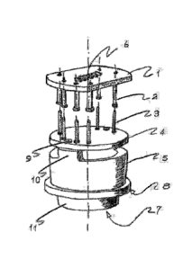
Reference is first made to figure 1, which shows elements of an embodiment of
the
invention being partially separated from each other, like in a "partially
exploded view"
drawing. A primary electronics board, which comprises a primary printed
circuit board 4,
PCB 4, fastened to a sensor housing 5 The PCB 4 is populated with various high
temperature electronic components and integrated circuits, and is for
connectivity
provided with a plurality of first connecting members 3, which are metal
connecting
members of a first gender that are connected and attached by high temperature
solder to
CA 02924338 2016-03-14
WO 2015/037998 PCT/N02014/050089
4
conducting paths or pads on the PCB 4. The first gender is preferably the male
gender,
meaning in respect of the present invention, that the first connecting
elements 3 are
advantageously elongated connector pins of relatively small diameter, hence
small cross
section, adapted to be received in hollow first connecting member of a second
gender in
order to create a complete electrical connection arrangement according to the
present
invention. Accordingly, in respect of the present invention, the first gender
is the male
gender. Consequently, the second gender is the female gender. For the high
temperature
electronic capacitive sensor to function properly and to deliver predictable,
stable and
reproducible measurements, the PCB 4 is fastened by first fasteners 9 to
raised portions
10 of one end of the housing 5, so as to be located as close as possible to
the dielectric
window 7 and the associated measuring capacitor plate electrode carried by the
window,
thereby minimizing thermal contact between the housing and the PCB 4, while
obtaining
stable electrical conditions within the sensor assembly and keeping a
centrally located
wire that connects the plate electrode to the electronics carried by PCB 4 as
short and
is stable as possible. A connector board, hereinafter referred to as the
secondary printed
circuit board 1, PCB 1, is provided with a plurality of second connecting
members 2,
which are metal connecting members of the second gender, meaning in respect of
the
present invention a female, hollow connector, such as e.g. a socket or sleeve,
adapted to
receive the male, pin shaped first connecting member of the first gender, in
order to
zo create a complete electrical connection arrangement according to the
present invention. In
the arrangement of the invention, the second connecting members 2 are
elongated metal
connecting members having an outer diameter, hence cross section, that is
substantially
larger than an outer diameter, hence cross section, of the first connecting
members 3. The
PCB 1 has conventional conductive paths adapted to connect the second
connecting
25 members 2 with conducting pads 6 to which conductors of a cable (not
shown) are
soldered. By the connection arrangement provided by the present invention,
heat
transferred from the sensor housing 5 to the conductive pads 6, via the high
temperature
PCB 4, the first male connecting members 3, the second female connecting
members 2
and the PCB 1, is considerably reduced, and conductors of a cable (not shown)
are
30 soldered to pads 6 by low temperature solder. By low temperature solder
is meant solder
used in commercial grade electronic equipment for operation in temperatures up
to about
130C. In the example illustrated in figure 1, six pads 6 have been shown.
Embodiments of the invention could rely on connecting elements that are well
known to a
35 person skilled in the art, and may favorably be with a cylindrical
geometry in a male-
female arrangement. In Figure 1 is further shown that the circuit board 4 may
typically be
CA 02924338 2016-03-14
WO 2015/037998 PCT/N02014/050089
attached to a metallic sensor housing 5, and the housing 5 having a collar
with a beveled
sealing surface 8, so that the sensor can sealingly mounted to a hole in a
wall of a sensor
hull or sensor container with a correspondingly beveled contact sealing
surface, so that
the dielectric window 7 having an electrode on its surface may contact the
medium in a
5 tank or a pipe in which the sensor has been installed, while the
electronics, the connecting
arrangement and cables attached thereto are kept isolated from the surrounding
medium
which is to be measured or characterized by measurements of the electric
capacitance of
the medium.
to Figure 2 shows an embodiment of the PCB1 subassembly part of a
connection
arrangement according to the invention in a further perspective view
illustration, having a
total of six pairs of conductive pads for insoldering cable and six
corresponding pairs of
holes for guiding cable and providing strain relief Each two pads 6 in a pair
of pads are
typically connected directly with each other, allowing for a power and signal
bus of up to
six conductors to be run through the PCB1 of one sensor unit and onto the PCB1
of a
next, adjacently located sensor unit. Thereby, a high temperature probe
comprising one or
more rows of adjacently located high temperature sensor units can be built
with a "daisy
chain" like electrical interconnecting arrangement, such as e.g. the exemplary
probe
assembly illustrated in figure 9, which accommodates two rows of sensor units
labeled
100 in a narrow, tubular probe housing labeled 400 having a probe sealing
flange 410 and
an "external" electronics housing 250 for accommodating therein further
electronic
circuitry and electric power supply U5, wherein each of the two rows includes
twelve
high temperature electronic capacitive sensor units with the connecting
arrangement of
the invention.
Figure 3 illustrates further details of the sensor housing 5, in particular
the raised portions
10 of the sensor housing for fastening the PCB 4 thereto, the cylindrical
sensor housing
"front" portion 11 to the inside of which the window is sealingly brazed, the
surrounding
collar portion of the housing having the beveled surface 8 to provide high
pressure and
high temperature proof sealing of the space at the "front" of the sensor with
dielectric
window from the space at the "back" of the sensor with plate electrode,
electronics,
connection arrangement and cables, and a race portion of the collar located
inside of the
beveled surface 6 and having a curved cross section for receiving a plurality
of spheres
that for part of a means for fastening the sensor housing to a circular
opening in a wall of
a hull or container in which the high temperature electronic capacitive sensor
is to be
mounted for making measurements of an electric capacitance of a medium that is
to be
6
measured or characterized.
Referring now to figure 4, further details of the sensor incorporating the
connection
arrangement according to the invention is shown, including the fasteners 9
employed for
attaching the PCB 4 to the raised portions 10 of the sensor housing 5 a
standoff member
14 for positioning the PCB 1 correctly with respect to the PCB 4 so as to keep
the
connecting members 2 and 3 properly aligned and in correct engagement with
each other
for establishing electrical connections and for establishing a controlled
thermal coupling,
and fastener 15 adapted for engagement with standoff member 14 for keeping PCB
1
u) properly positioned and fixated with respect to the PCB 4 and the sensor
housing 5. In
this figure 4 is also indicated the location of the race 13 which forms a
circular path
around the collar, and is adapted to receive a plurality of spheres for
applying an evenly
distributed force on the collar and on the sealing surface 8 of the sensor
housing.
is Referring now to figure 5, the high temperature electronic capacitive
sensor unit
comprising the connecting arrangement of the invention is shown in a further
perspective
view, showing more of the race 13 encircling the main body of the sensor
housing 5.
Referring now to figure 6, the high temperature electronic capacitive sensor
unit
20 comprising the connecting arrangement of the invention is shown in a
further perspective
view, showing more of the positions of the PCB 1 and the PCB 4 relative to
each other
and to the sensor housing 5 and the dielectric window 7, for providing stable,
well
shielded and controlled electrical conditions for the capacitive measurements
involving
the electrode on the window 7 and the electronics of the PCB 4, while
providing
25 connectivity via soldering pads 6 to which a bus cable is soldered and
low thermal
coupling between the sensor housing 5 and the connections made on PCB 1.
Referring now to figure 7, more details of the arrangement for fastening the
high
temperature electronic capacitive sensor unit to a wall of a hull, container
or probe
30 housing is shown, including a threaded retainer ring 17 having threads
on a
circumference that are adapted for engagement with corresponding threads
provided on
an inner surface of a hole in the wall that is to receive and accommodate the
high
temperature electronic capacitive sensor unit sealingly attached to the hull,
container or
probe housing. In this figure 7, the PCB 1, the PCB 4 and fastener and
standoff members
35 are not shown. the retainer ring is shown carrying a plurality of
spheres, typically steel
spheres, on a circular race formed in an upper surface of the ring, which race
corresponds
Date Recue/Date Received 2020-12-08
CA 02924338 2016-03-14
WO 2015/037998 PCT/N02014/050089
7
to the race 13 formed in the collar portion of the sensor housing 5. The ring
17 carrying
the spheres 16 is in this figure 7 shown separated from the housing, which
corresponds to
an interim relative positioning of these members during installation of the
sensor unit,
and it will be understood that when the high temperature electronic capacitive
sensor unit
comprising the connecting arrangement of the invention has been installed in
the wall, the
spheres 16 are in contact with both the race 13 in the collar of the sensor
housing 5 and
the race formed in the retainer ring 17.
Referring now to figure 8A, the details of the arrangement for fastening the
high
io temperature electronic capacitive sensor unit to a wall of a hull,
container or probe
housing that were illustrated in figure 7 are in this figure 8A shown in a
cross section
view. Accordingly, the shape of race 19 arranged in the retainer ring 17 to
receive the
spheres 16 is made visible, while the spheres are shown "levitated" in a space
between
the race 9 and the race 13 not to occlude the illustration of these races. It
will be
is understood that the retainer ring 17 has an opening that is dimensioned
for allowing the
retainer ring 17 to pass over the window holding portion 11 of the sensor
housing 5.
Referring now to figure 8B, the details of parts of the arrangement for
fastening the high
temperature electronic capacitive sensor unit to a wall of a hull, container
or probe
zo housing that were illustrated in figure 8A shown in an enlarged cross
section view, for a
better understanding of the cross section profiles of the races 13 and 19 as
adapted to
receive the spheres 16, so as to allow a retention force applied by the
retainer ring as its
threads are engaged in threads of a wall to which the sensor unit is mounted
to become a
purely axial force, and no tangential force is coupled from the retainer ring
during its
25 rotation when torqued to fasten the sensor in a circular hole in the
wall.
Referring now to figure 8C, further the details of parts of the arrangement
for fastening
the high temperature electronic capacitive sensor unit to a wall of a hull,
container or
probe housing similar to what has been illustrated in figures 8A and 8B are
shown in an
30 enlarged cross section view, now with the high temperature electronic
capacitive sensor
unit completely installed and fixedly mounted in the wall 20 of a hull,
container or probe
housing, such as e.g. a wall of the tubular probe housing 400 illustrated in
figure 9. In this
embodiment being illustrated in figure 8C, an improved sealing arrangement has
been
implemented, comprising also a metallic sealing member 21 which is arranged
between a
35 ring shaped surface of the wall 20, which ring shaped surface has a
diameter that
corresponds closely to that of the collar portion of the sensor housing 5, and
the shape
CA 02924338 2016-03-14
WO 2015/037998 PCT/N02014/050089
8
and overall diameter of the beveled or aslant (frustoconical) surface 8 of the
collar
portion. The threaded outer portion 18 of the retainer ring 17 is well engaged
in a
correspondingly threaded portion of the wall 20, so as to apply a force on the
spheres 16
that is being coupled in a direction that is substantially purely
perpendicular to the race or
raceway surface 13 of the collar portion of the sensor housing 5 and the race
or raceway
surface 19 of the retainer ring 17. Thereby, the no special arrangement is
required in
order to keep the high temperature electronic capacitive sensor unit
comprising the
connecting arrangement of the invention in a desired position in the wall 20
when a high
torque is being applied to the retainer ring 17 for obtaining a reliable high
pressure, high
io temperature sealing at the sealing member 21, and any risk of damage to
cables soldered
to the PCB 1 due to relative rotation of the sensor unit the high temperature
electronic
capacitive sensor unit comprising the connecting arrangement of the invention
relative to
the wall 20 has been eliminated.
CA 02924338 2016-03-14
WO 2015/037998
PCT/N02014/050089
9
Reference numerals:
1 Secondary printed circuit board - PCB
2 Second metal connecting member of a second gender
3 First metal connecting member of a first gender
4 Primary printed circuit board ¨ PCB
5 Sensor housing
6 Pad for insoldering cable
7 Dielectric window with plate electrode surface
8 Sealing surface on collar
9 Fastener for primary PCB
10 Raised sensor housing portion
11 Window holding portion of sensor housing
12 Cable guiding hole
is 13 Ball / sphere race / raceway portion of sensor mounting collar
14 Standoff mount for secondary PCB
Fastener for secondary PCB
16 Ball / sphere
17 Threaded retaining ring
zo 18 Threaded (outside) portion of threaded retaining ring
19 Ball / sphere race / raceway portion of threaded retaining ring
Wall of hull, container or probe housing (400)
21 Sealing member
300 Medium to be characterized or measured