Note: Descriptions are shown in the official language in which they were submitted.
CA 02924626 2016-03-17
270081
INVERTER WITH IMPROVED SHOOT THROUGH IMMUNITY
BACKGROUND OF THE INVENTION
[0001] The invention pertains generally to the field of electrical power
conversion and
particularly to DC to AC inverters utilizing semiconductor switches.
[0002] Electrical power inverters typically utilize pairs of semiconductor
switches that
are connected together across a DC bus or supply lines to which a DC voltage
source is
connected. The switches are alternately turned on and off in a selected
switching sequence to
provide AC power to a load connected to a node between the two switches. The
high side
semiconductor switches are almost always selected to be n-type devices because
of their
superior switching characteristics and low on-resistance compared to p-type
devices. As a
result, the high side switch requires a floating voltage source and level-
shift function that
contributes to the cost and complexity of the inverter gate drive. A single
pair of
semiconductor switches connected in this manner may be used by itself to
provide single
phase AC power to a load, or two pairs of switches may be connected together
in a
conventional H-bridge configuration, for single phase power, three pairs of
switches for three
phase power, etc. Each pair of switches may be considered a phase leg of a
single phase or
multiphase inverter.
[0003] Dead time is almost always added to the gate drive signals provided
to the two
switches of a phase leg to ensure that one of the switches is completely
turned off before the
other switch is turned on. Otherwise, if both of the switches were turned on
simultaneously,
a short circuit current through the switches could burn out the switches or
damage other
circuit components because the two switches are connected in series across the
DC bus lines.
This condition is sometimes called "shoot through." However, the presence of
dead time can
add a significant amount of undesired non-linearity and harmonic distortion to
output voltage
waveforms. The output waveform distortion and voltage amplitude loss of the
fundamental-
frequency components becomes worse as either the fundamental frequency or the
carrier
frequency increases.
CA 02924626 2016-03-17
270081
[0004] Different methods for compensating for dead time are known,
including sensing
current flow through the switches and ensuring the turn-off of a conducting
switch before
the other is turned on. See U.S. Pat. Nos. 4,126,819, 5,646,837 and 5,859,519
and published
U.S. patent application US2001/0048278A1. Such circuits require significant
additional
components, with significant added cost, or still require delays between turn-
off and turn-on
of the switches with corresponding dead time. U.S. Patent No. 6,909,620 has an
output node
between the two switches, with a series diode or connector switch between the
output node
and the low side switch, and the junction between the diode or connector
switch and the low
side switch electrically connected directly to the gate of the high side
switch. If the low side
switch is still conducting at the time that the high side switch receives a
command to turn on,
the gate of the high side switch will be biased so that the switch is held off
until current stops
flowing through the low side switch and, conversely, if the high side switch
is still on at the
time that the low side switch is turned on, the gate of the high side switch
will be biased to
insure its immediate turn-off, thereby preventing a condition under which the
high side and
low side switches are turned on at the same time.
[0005] Yet as the fast switching of the high speed switches occurs, the
drain-gate
capacitance creates a path for parasitic current to flow into the internal
gate resistance, which
causes a voltage spike on the gate, risking unwanted turn on, and a shoot
through condition
to possibly occur.
BRIEF DESCRIPTION OF THE INVENTION
[0006] One aspect of the invention relates to an inverter phase leg
comprising a high
supply line and a low supply line across which a DC voltage may be provided.
The inverter
leg includes a high side gate controlled switch connected to the high supply
line and a low
side gate controlled switch connected to the low supply line. The switches are
connected
between the high supply line and the low supply line with an output node
between the high
side switch and the low side switch. An inverting driver is connected to the
high side gate
controlled switch and has an input voltage from a control signal, an output
voltage for
switching the high side gate controlled switch, and a driving voltage. A
source of first DC
voltage is provided between the output node and the inverting driver. The
driving voltage is
set to cause the output voltage of the inverting driver to be zero until the
input voltage
exceeds the first DC voltage, thereby preventing a shoot through condition
caused by
uncontrolled activation of the high side gate controlled switch.
2
CA 02924626 2016-03-17
270081
BRIEF DESCRIPTION OF THE DRAWINGS
[0007] In the drawings:
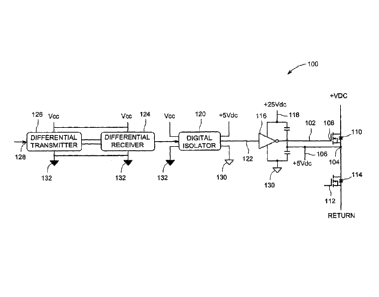
[0008] FIG. 1 is a schematic of a single phase DC to AC inverter.
[0009] FIG. 2 is a schematic of a three phase DC to AC inverter.
[0010] FIG. 3 is a schematic of an isolation circuit for any one of the
phase legs in the
inverters of FIGS. 1 and 2.
DESCRIPTION OF EMBODIMENTS OF THE INVENTION
[0011] In the background and the following description, for the purposes of
explanation,
numerous specific details are set forth in order to provide a thorough
understanding of the
technology described herein. It will be evident to one skilled in the art,
however, that the
exemplary embodiments may be practiced without these specific details. In
other instances,
structures and devices are shown in diagram form in order to facilitate
description of the
exemplary embodiments.
[0012] FIG. 1 is a schematic of a single phase DC to AC inverter 10 of the
type in which
the invention may be practiced. The DC to AC inverter 10 includes a high side
supply line
12 shown as a +VDC source and a low side supply line 14 shown as a ground or
return.
Both supply lines 12, 14 are supplied with power from a DC power supply (not
shown) that is
configured to provide an appropriate DC output voltage across the supply lines
12, 14. The
DC to AC inverter 10 further includes a pair of inverter phase legs 100, each
inverter phase
leg having two gate controlled semiconductor switches connected in series
across the supply
lines 12, 14. The two gate controlled semiconductor switches may be insulated
gate bipolar
transistors (IGBTs) or power MOSFETs, or bipolar transistors, or the like. An
output node
104 between the two gate controlled semiconductor switches in one inverter
phase leg 100 is
connected to an output line 16 on which the AC output voltage of the DC to AC
inverter 10 is
provided. A second output node 104 between the two gate controlled
semiconductor
switches in another inverter phase leg 100 is connected to an output line 18
which serves as
a neutral line for the AC output voltage. A gate drive line 102 connects the
gate input of each
of the high side gate controlled semiconductor switches to an inverting driver
(not shown in
FIG. 1) in accord with the invention as explained below.
3
CA 02924626 2016-03-17
270081
[0013] FIG. 2 is a schematic of a three phase DC to AC inverter 20 of the
type in which
the invention may be practiced. The DC to AC inverter 20 includes a high side
supply line
22 shown as a +VDC source and a low side supply line 24 shown as a ground or
return.
Both supply lines 22, 24 are supplied with power from a DC power supply (not
shown) that is
configured to provide an appropriate DC output voltage across the supply lines
22, 24. The
DC to AC inverter 20 further includes four inverter phase legs 100, each
inverter phase leg
having two gate controlled semiconductor switches connected in series across
the supply
lines 22, 24. The two gate controlled semiconductor switches may be insulated
gate bipolar
transistors (IGBTs) or power MOSFETs, or bipolar transistors, or the like. An
output node
104 between the two gate controlled semiconductor switches in each inverter
phase leg 100
is connected to an output line 26, 28, 30, and 32, respectively. Three of the
lines 26, 30, and
32 provide the three voltage phases of the three phase AC output voltage and
one of the lines
28 provides a neutral. A gate drive line 102 connects to the gate input of
each high side gate
controlled semiconductor switch.
[0014] The gate drive line 102 carries a one bit signal out of a
controlling device (not
shown in FIGS. 1 and 2). This signal must traverse board traces, cabling, and
other
components to get to the high speed gate controlled semiconductor switches,
all of which
which results in noise, transient voltages, and parasitic currents.
Consequently electrical
isolation between the switches and the control circuitry is desired. Also,
with many systems,
the duty cycles can vary from 0 to 100%. Such a wide window of duty cycles
makes
conventional gate drive transformers ineffective as isolation barriers.
[0015] FIG. 3 is a schematic of an inverter phase leg 100 according to the
invention as
might be used in a DC to AC inverter 10, 20 of FIGS. 1 and 2. The phase leg
100 comprises
a high side supply line +VDC and a low side supply line return across which a
DC voltage
may be provided. A high side gate controlled switch 110 with a gate 108 is
connected to the
high supply line, and a low side gate controlled switch 114 with a gate 112 is
connected to
the low supply line. An output node 104 between the gate controlled switches
110, 114 is
connected to the output voltage as shown in FIGS. 1 and 2.
[0016] Some isolation may be provided by a differential transmitter 126 and
a
differential receiver 124 which receive a gate drive signal 128 from a
controller (not shown).
A differential transmitter 126 and a differential receiver 124 are beneficial
when transmitting
the gate drive signal 128 over distances. Even though capacitive coupling
throughout the
4
CA 02924626 2016-03-17
270081
system during the switching of the gate controlled switches 110, 114 can
couple noise into
the circuitry or wiring, the fact that the signals are differential provides a
good level of
immunity, allowing good signal integrity to be kept.
[0017] Further isolation may be provided by a high speed digital isolator
120 that can
effectively maintain the resolution of the gate drive signal 128.
Nevertheless, some
capacitive coupling into the output line 122 from the isolator 120 may still
cause spurious
transient switching of the gate controlled switches 110, 114. The problem
primarily occurs
on the high side gate controlled switch 110, due to the potential of its
source operating
between zero and full input voltage. When the high side gate controlled switch
110 turns off,
its source flies down. Capacitive coupling into the isolator's internal
secondary resistance
causes the isolator's output voltage to go up. This tendency of the isolator
output line 122 to
go up from zero would cause the voltage at the gate 108 to tend upwards, which
can turn on
the high side gate controlled switch 110 before the low side gate controlled
switch 114 turns
completely off, causing shoot through, especially as the system input voltage
grew higher.
[0018] The problem is completely eliminated by an inverting driver 116
between the
isolator 120 and the high side gate controlled switch 110 to modulate the gate
drive signal
128. Preferably, a driving voltage for the inverting driver 116 provides a
modulation range
for the gate drive signal 128 of 25V from a lower DC voltage at 130 of -5V to
an upper DC
voltage at 118 of +20V. The lower and upper DC voltages 130, 118 can be
supplied by two
independent regulated power supplies (not shown), or a single 25V supply.
Preferably, the
output node 104 supplies a biasing DC voltage 106 to the driving voltage that
to ensure the
lower and upper DC voltages 130, 118 balance themselves correctly. Using the
same DC
supply from the node 104 that is used for the logic level signals of the gate
controlled
switches 110, 114 ensures that the high side gate controlled switch 110 is
well biased off
before the gate driver becomes active, one means of such is to use this logic
level power to
control a switch (not shown) between the source of the driver's voltage and
the Inverting
Driver power pins which will be held off until the logic voltage reaches a
level near its
steady state regulation level.
[0019] This negative bias voltage across the gate drive line 102 when the
high side gate
controlled switch 110 is off prevents harmful transient-induced turn-on by
increasing the
amount of spurious voltage that must be generated in order to turn on the high
side gate
controlled switch 110 improperly. This structure, in turn, allows the high
side gate controlled
CA 02924626 2016-03-17
270081
switch 110 to be switched at the highest speeds possible. The negative bias
also helps to turn
off the high side gate controlled switch 110 harder during normal operation.
[0020] This
written description uses examples to disclose the invention, including the
best mode, and also to enable any person skilled in the art to practice the
invention, including
making and using any devices or systems and performing any incorporated
methods. The
patentable scope of the invention may include other examples that occur to
those skilled in
the art in view of the description. Such other examples are intended to be
within the scope
of the invention.
6