Note: Descriptions are shown in the official language in which they were submitted.
CA 02924766 2016-03-18
1
DESCRIPTION
SECONDARY BATTERY AND METHOD OF MANUFACTURING THE SAME
TECHNICAL FIELD
[0001] The present invention relates to a secondary
battery and a method of manufacturing the same, and for example,
relates to a secondary battery (hereinafter, called a quantum
battery as well) based on an operational principle of forming
a new energy level in a band gap and capturing an electron
by utilizing a photoexcited structural change of a metal
oxide.
BACKGROUND ART
[0002] There have been known nickel-metal hydride
(Ni-MH) batteries, lithium ion secondary batteries (LIB), and
the like as secondary batteries. Recently, there is a need
for small and high-capacity batteries. Accordingly, in some
cases, a plurality of units (hereinafter, called unit cells)
each functioning as a secondary cell are superposed.
[0003] Structures of a cylindrical type and a rectangular
type of nickel-metal hydride (Ni-MH) batteries as illustrated
in FIGs. 1 and 2 are disclosed on pages 319-320 in Non-Patent
Document 1. A cylindrical type battery 1A is completed as
a battery by winding a positive electrode 2 and a negative
electrode 3 each being thin-plate-shaped to have a
predetermined shape in whorl via a separator 4 (the whorl being
perceived as superposed unit cells), inserting the whorl into
a cylindrical case 5, and performing sealing after an
electrolyte is poured therein. A rectangular battery 1B is
completed as a battery by layering structures each having a
separator 4 between a positive electrode 2 and a negative
CA 02924766 2016-03-18
2
electrode 3 each being thin-plate-shaped to have a
predetermined shape, inserting the structures into a
rectangular case 5, and performing sealing after an
electrolyte is poured therein.
[0004] In Patent Document 1, there is disclosed an
internal structure (electrode plate group) of a rectangular
lithium ion secondary battery as illustrated in FIG. 3. In
the electrode plate group 1C, positive electrode plates 2 and
negative electrode plates 3 are alternately inserted to
valley grooves of a continuous body of a zigzag-folded
separator 4 and flattened by being pressed in a zigzag
direction. Such an electrode plate group is inserted into
a rectangular external enclosure and sealing is performed
after an electrolyte is poured therein to complete a
rectangular battery.
[0005] Further, recently, all-solid-state secondary
cells structured with solid thin films have been researched
and developed as being expected to actualize downssized
secondary cells. FIG. 4 is a perspective view and a sectional
view illustrating a structure of an all-solid-state secondary
cell. In FIG. 4, terminal members such as a positive
electrode terminal and a negative electrode terminal,
mounting members such as an external member and a cover member,
and the like are not illustrated. An all-solid-state
secondary cell 10 includes a solid layer (hereinafter, called
a storage layer) 6 in which internal change occurs during
charging and discharging between a negative electrode layer
3 and a positive electrode layer 2. Examples of the
all-solid-state secondary cell 1D include a quantum cell
described above and an all-solid-state lithium ion secondary
CA 02924766 2016-03-18
3
cell. Ina case of a quantum cell, a layer (called a charging
layer as described later) to store (capture) electrons with
a charging operation and to release the charged electrons with
a discharging operation is arranged between the negative
electrode layer 3 and the positive electrode layer 2. The
charging layer corresponds to the storage layer 6. In a case
of the all-solid-state lithium ion secondary cell, a solid
electrolyte layer is arranged between the negative electrode
layer 3 and the positive electrode layer 2. The solid
electrolyte layer corresponds to the storage layer 6. Here,
in a case that the structure illustrated in FIG. 4 is to be
layered as a unit cell, it is preferable that a seal V is
arranged around the storage layer 6 and the like for providing
insulation between the negative electrode layer 3 and the
positive electrode layer 2 and for protecting the periphery
of the storage layer 6. Here, the seal 7 is not an essential
structural element.
[0006] As is widely known, regarding the all-solid-state
secondary cell 1D as well, terminal voltage can be heightened
by layering unit cells in series and energy density can be
increased by layering unit cells in parallel.
[0007] FIG. 5 is a sectional view illustrating an
easily-anticipatable secondary battery lE in which a
plurality of unit cells are parallel-connected with each unit
cell being the secondary cell 1D. In the secondary battery
1E, each unit cell 1D is sandwiched between the negative
electrode terminal plate 8 and the positive electrode
terminal plate 9, and further, an insulation layer 1C is
arranged between the positive electrode terminal plate 9 of
a unit cell and the negative electrode terminal plate 8 of
CA 02924766 2016-03-18
4
a unit cell at the one-stage upper side therefrom. A
plurality of the negative electrode terminal plates 8 are
connected by a negative electrode terminal connection portion
8b and a plurality of the positive electrode terminal plates
9 are connected by a positive electrode terminal connection
portion 9b. The negative electrode terminal connection
portion 8b and the positive electrode terminal connection
portion 9b include extension portions 8a, 9a, respectively,
for exposing the negative electrode terminal and the positive
electrode terminal to the outside of a mounting member (not
illustrated). Assuming that the secondary cell 1D has
terminal voltage Vo and current capacity To, and the number
(parallel-connected number) of layers of the secondary cells
1D is N, capacity of the secondary battery lE becomes to N
x lo (e.g., 610 if the number of layers is six) while terminal
voltage thereof remains at Vo.
[0008] To actualize a secondary battery having high
terminal voltage and large energy density, unit cells are
simply required to be arranged in combination of a multilayer
in serial connection and a mult i 1 ayer in parallel connection.
Here, for example, owing to that a unit cell 117 sandwiched
between the negative electrode terminal plate 8 and the
positive electrode terminal plate 9 in FIG. 5 is replaced with
a multi layer of a plurality of unit cells in serial connection,
it is possible to structure a secondary battery having higher
terminal voltage and larger energy density.
CITED DOCUMENT
PATENT DOCUMENT
[0009] Patent Document 1: Japanese Patent Application
Laid-Open No. 2009-140707
CA 02924766 2016-03-18
NON-PATENT DOCUMENT
[0010] Non-Patent Document 1: Committee of Battery
Technology in Electrochemical Society (February 2010):
Battery handbook. Ormsha, Ltd.
SUMMARY OF THE INVENTION
[0011] In the conventional secondary battery illustrated
in FIGs. 1 to 3, it is required to arrange a separator for
providing insulation between a positive electrode and a
negative electrode of adjacent unit cells and to ensure
accommodation space for an electrolyte. Accordingly, it has
been difficult to reduce whole volume of the secondary battery.
In the secondary battery illustrated in FIGs. 1 to 3, since
chemical reaction is utilized, deterioration of
charging/discharging performance and reduction of lifetime
may be caused. Further, since an electrolyte is used, there
may be a risk of fluid leakage. Furthermore, in a lithium
ion secondary battery, there is a fear of reliability
degradation due to overcharging and charging/discharging,
and short-circuit occurrence between electrodes due to usage
of an electrolyte.
[00123 Most of problems caused by using an electrolyte
can be solved by using an all-solid-state secondary cell.
[0013] As described above, energy density of a secondary
battery can be increased by parallel-connecting a plurality
of unit cells. However, in the secondary battery lE as
illustrated in FIG. 5, it is required to arrange an insulation
layer 10 between the negative electrode terminal plate 8 and
the positive electrode terminal plate 9 of adjacent unit cells.
Further, it is required to arrange the negative electrode
terminal plates B as the same number of the negative electrode
CA 02924766 2016-03-18
6
layers 3 of the unit cells and to arrange the positive
electrode terminal plates 9 as the same number of the positive
electrode layers 2 of the unit cells. Accordingly, volume
of the secondary battery lE is increased.
[00141 In general, volume efficiency of a battery is
obtained as a ratio of effective volume of the battery to whole
volume of the battery. In consideration of cycles of charging
a secondary battery, it is required for the secondary battery
to have large energy density. Here, it is preferable that
whole volume of the battery is small even though energy density
is increased. Further, reduction of whole volume of the
battery contributes to downsizing of the secondary battery.
Here, the negative electrode terminal plates 8 and the
positive electrode terminal plates 9 are necessary for
structuring a battery. However, due to no direct
contribution to charging, the insulation layers 10 are
obstructive factors for increasing energy density.
[0015] It is possible to increase the number of layers
of unit cells in parallel connection in accordance with
increase of desired energy density. However, the number of
the insulation layers 10 is increased (as well as the number
of the negative electrode terminal plates 8 and the positive
electrode terminal plates 9) in accordance with increase of
the number of layers. As a result, whole volume is further
increased.
[0016] In either parallel connection or serial
connection, a secondary battery in which a plurality of unit
cells are layered has high requirements for positioning of
the respective unit cells. In a case of the secondary battery
lE illustrated in FIG. 5, it is preferable, from a viewpoint
CA 02924766 2016-03-18
_
7
of reducing whole volume, that the negative electrode
terminal connection portions 8b and the positive electrode
terminal connection portions 9b are arranged closer to the
unit cells 1D (i.e., a gap L in FIG. 5 is smaller). For example,
if any of the unit cells is layered as being shifted rightward
in FIG. 5 and the negative electrode layer 3 of the unit cell
is contacted to the positive electrode terminal connection
portion 9b, a short-circuit is formed thereat. Thus, the
respective unit cells have high requirements for positioning.
Accordingly, there may be a possibility to cause decrease of
manufacturing efficiency.
[0017] Further, owing to that unit cells as the number
of layers have to be layered in a layering process, there has
been large workload for manufacturing.
[0018] In such a situation, there has been desired an
all-solid-state secondary battery and a method of
manufacturing the same in which a storage layer is sandwiched
between a positive electrode layer and a negative electrode
layer and which has high energy density and less manufacturing
processes.
[0019] To solve such problems, a secondary battery as a
first invention includes (1) a sheet-shaped
first-electrode-functioning base material having a function
as a first electrode and a function as a base material, (2)
, a front-side storage layer formed on a front side of the
first-electrode-functioning base material, (3) a front-side
second electrode layer layered on the front-side storage
layer, (4) a rear-side storage layer formed on a rear side
of the first-electrode-functioning base material, and (5) a
rear-side second electrode layer layered on the rear-side
8
storage layer.
[0020] A method of manufacturing a secondary battery as
a second invention includes (1) layering a first oxide
semiconductor layer respectively on a front side and a rear
side of a sheet-shaped first-electrode-functioning base
material having a function as a first electrode and a function
as a base material, (2) layering a front-side charging layer
on the front-side first oxide semiconductor layer, (3)
layering a rear-side charging layer on the rear-side first
oxide semiconductor layer, (4) irradiating the front-side
charging layer and the rear-side charging layer with
ultraviolet light, (5) layering a second oxide semiconductor
layer and a second electrode layer on the front-side charging
layer, and (6) layering a second oxide semiconductor layer
and a second electrode layer on the rear-side charging layer.
[0021] A method of manufacturing a secondary battery as
a third invention includes (1) layering a first oxide
semiconductor layer continuously from a front side to a rear
side of a sheet-shaped first-electrode-functioning base
material having a function as a first electrode and a function
as a base material, (2)layering a charging layer to cover a
part or all of the first oxide semiconductor layer, (3)
irradiating the charging layer with ultraviolet light, and
(4) layering a second oxide semiconductor layer and a second
electrode layer to cover a part or all of the charging layer.
[0022] According to the secondary battery and the method
for manufacturing the same of the present invention, the
single first electrode layer (first-electrode-functioning
base material) functions as first electrode layers of two unit
cells that are formed at mutually-opposite sides thereagainst.
CA 2924766 2017-08-17
9
1
Therefore, energy density can be increased owing to that
thickness of the first electrode layer can be effectively
halved while maintaining strength as the base material.
Further, since two unit cells can be formed with single
manufacturing of the first electrode layer
(first-electrode-functioning base material), there arises
another effect of reducing manufacturing processes.
[0023] Further, owing to that the single first electrode
layer (first-electrode-functioning base material) functions as
first electrode layers of two unit cells that are formed at
mutually-opposite sides thereagainst, a process of connecting
the first electrode layers can be eliminated when the two unit
cells are to be parallel-connected. Accordingly, there arises
another effect of preventing oxidation at a layered portion
due to thermal treatment during the process.
BRIEF DESCRIPTION OF THE DRAWINGS
[0024] FIG. 1 is a perspective view illustrating an
internal structure of a conventional cylindrical nickel-
metal hydride (Ni-MH) battery with a part thereof broken.
FIG. 2 is a perspective view illustrating an internal
structure of a conventional rectangular nickel-metal hydride
(Ni-MH) battery with a part thereof broken.
FIG. 3 is a perspective view illustrating an internal
structure (electrode plate groups) of a rectangular lithium ion
secondary battery disclosed in Patent Document 1.
FIG. 4A is a perspective view illustrating a
structure of an all-solid-state secondary cell.
FIG. 4B is a sectional view illustrating a structure
, of an all-solid-state secondary cell.
FIG. 5 is a sectional view illustrating an anticipatable
CA 2924766 2017-08-17
10
structure of a secondary battery in which a plurality of unit
cells are parallel-connected with each unit cell being an all-
solid-state secondary cell.
FIG. 6 is a sectional view illustrating a structure of a
secondary battery of a first embodiment.
FIG. 7A1 is a first sectional view illustrating the first
step in a method of manufacturing a secondary battery of the
first embodIment.
FIG. 7A2 is a first sectional view illustrating the
second step in a method of manufacturing a secondary battery
of the first embodiment.
FIG. 7A3 is a first sectional view illustrating the third
step in a method of manufacturing a secondary battery of the
first embodiment.
FIG. 7A4 is a first sectional view illustrating the
fourth step in a method of manufacturing a secondary battery
of the first embodiment.
FIG. 7B1 is a second sectional view illustrating the
first step in a method of manufacturing a secondary battery of
the first embodiment.
FIG. 7B2 is a second sectional view illustrating the
second step in a method of manufacturing a secondary battery
of the first embodiment.
FIG. 7B3 is a second sectional view illustrating the
third step in a method of manufacturing a secondary battery of
the first embodiment.
FIG. 7B4 is a second sectional view illustrating the
fourth step in a method of manufacturing a secondary battery
of the first embodiment.
FIG. 8A is a plane view illustrating an example of a
mounting structure of a second secondary battery of the first
embodiment.
FIG. 8B is a perspective view viewing the section along
line VIIIB-VIIIB in Figure 8A from the upper side.
FIG. 8C Illustrates a state wherein the exposed negative
CA 2924766 2017-08-17
10A
electrode member and the exposed positive electrode member are
attached to the wound roll.
FIG. 8D illustrates the side face of an approximately
cylindrical state covered with a sheet-shaped insulating member.
FIG. 9A illustrates a modified embodiment of an end face
insulating member of a secondary battery of the first
embodiment.
FIG. 9B illustrates an alzernative modified embodiment of
an end face insulating member of a secondary battery of the
first embodiment.
EMBODIMENTS OF THE INVENTION
[0025) (A) First embodiment
In the following a first embodiment of a secondary
battery and a method of manufacturing the same will be
described with reference to the drawings. The secondary
battery of the first embodiment is structured as a quantum
battery.
(00261 (A-1) Basic structure of secondary battery of
first embodiment
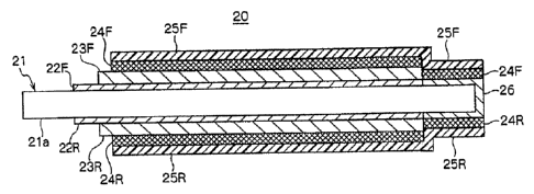
4
FIG. 6 is a sectional view illustrating a structure of a
secondary battery 20 according to the first embodiment as
viewing from the same direction as FIG. 4(B) In
FIG. 6,
dimensions in the thickness direction are more emphasized
than those in the planer direction.
[0027] As
illustrated in FIG. 6, the secondary battery
20 of the first embodiment includes a sheet-shaped
negative-electrode-functioning base material 21, a
CA 2924766 2017-08-17
11
front-side n-type metal oxide semiconductor layer 22F, a
front-side charging layer 23F, a front-side p-type metal
oxide semiconductor layer 24F, a front-side positive
electrode layer 25F, a rear-side n-type metal oxide
semiconductor layer 22R, a rear-side charging layer 23R, a
rear-side p-type metal oxide semiconductor layer 24R, a
rear-side positive electrode layer 25R, and a base material
end face insulating portion 26.
[0028] A unit secondary cell (unit cell) at the front side
is structured with the sheet-shaped
negative-electrode-functioning base material 21, the
front-side n-type metal oxide semiconductor layer 22F, the
front-side charging layer 23F, the front-side p-type metal
oxide semiconductor layer 24F, and the front-side positive
electrode layer 25F. Further, a unit secondary cell (unit
cell) at the rear side is structured with the sheet-shaped
1
negative-electrode-functioning base material 21, the
rear-side n-type metal oxide semiconductor layer 22R, the
rear-side charging layer 23R, the rear-side p-type metal
oxide semiconductor layer 24R, and the rear-side positive
electrode layer 25R.
[0029] The secondary battery 20 has a feature that unit
cells are formed respectively on both faces of the base
material. Here, it is not distinguishable which face of both
the faces is the front side. In the following description,
the upper face in FIG. 6 is called the front side and the lower
face in FIG. 6 is called the rear side, for convenience.
Further, in the following, description is provided on the
secondary battery 20 that is shaped as a rectangular sheet
as having a large length difference between a short side and
CA 2924766 2017-08-17
12
a long side (see FIG. 7 descried later). When appropriate,
the lateral direction in FIG. 6 is called a width direction
and the normal direction to the depiction of FIG. 6 is called
an elongated direction.
[0030] The sheet-shaped negative-electrode-functioning
base material 21 functions as a sheet-shaped base material
when a thin-film forming process is performed as well as a
negative electrode main body. FIG. 4 illustrating the
abovementioned conventional secondary cell (quantum cell) 1D
illustrates a secondary cell that is obtained by being removed
from a base material after a variety of thin-film forming
processes are performed on the base material. Compared to
the conventional secondary cell (quantum cell) 1D, the
secondary battery 20 of the first embodiment has a feature
that a single negative electrode layer (the sheet-shaped
negative-electrode-functioning base material 21) functions
as negative electrode layers for two unit cells that are
plane-symmetrical with respect thereto. One end (the left
end in FIG. 6) 21a in the width direction of the sheet-shaped
negative-electrode-functioning base material 21 (lateral
direction in FIG. 6) functions as a leading portion of the
negative electrode without being covered with the n-type
metal oxide semiconductor layers 22F, 22R, the charging
layers 23F, 23R, the p-type metal oxide semiconductor layers
24F, 24R, and the positive electrode layers 25F, 25R.
[0031] The sheet-shaped negative-electrode-functioning
base material 21 may be formed of a single conductive material
or may be formed by depositing a conductive thin film onto
a surface of a conductor or an insulator with sputtering,
plating or the like. For example, a stainless steel sheet
CA 2924766 2017-08-17
CA 02924766 2016-03-18
13
(SUS sheet) may be used as the sheet-shaped
negative-electrode-functioning base material 21.
[0032] The charging layers 23F, 23R at both sides are
layers to store electrons with a charging operation, to
release the stored electrons with a discharging operation,
and to hold (store) the electrons in a state without charging
and discharging performed. For causing the charging layers
to function as described above, for example, as disclosed in
International Patent Application Laid-open No. W02008/053561,
it is simply required to form trap levels in a band gap in
the charging layer based on photoexcited structural change.
Here, translucent metal oxide being a semiconductor having
a predetermined value or more of a band gap forms a charging
layer in which the metal oxide insulation-coated in a
particulate state forms a layer. When electrons in a valence
band are excited into a conduction band by being irradiated
with ultraviolet light, a part of the electrons are moved to
a negative electrode through an energy barrier formed of an
insulation film. Accordingly, an electron-absent depletion
level is moved into the band gap owing to structural change
that an interatomic distance is varied at the part from 'which
electrons in the charging layer are removed, so that the trap
level is formed. After a number of trap levels are formed
in the band gap by irradiation with a sufficient amount of
light, a positive electrode is arranged at the opposite side
of the charging layer to the negative electrode through the
energy barrier formed of an insulator or the like. Then, when
a voltage is applied between both the electrodes, charging
and discharging can be performed with capturing and releasing
of electrons at the trap levels. This is the function of the
CA 02924766 2016-03-18
14
charging layer in a quantum cell.
[0033] The n-type metal oxide semiconductor layer 22F,
22R at each side has a function of an energy barrier at the
charging layer 23F, 23R as being similar to an insulation layer
around the metal oxide. Accordingly, it is possible to
prevent occurrence of a portion where the energy barrier does
not exist due to direct contact of the metal oxide with the
negative electrode for some reason not through an insulation
layer. A material of the n-type metal oxide semiconductor
layers 22F, 22R is not limited. For example, titanium dioxide
(TiO2) may be used therefor.
[0034] When a quantum battery is recognized as being
structured with a portion to hold electric energy and two
electrodes as being similar to a general secondary battery,
the n-type metal oxide semiconductor layers 22F, 22R can be
regarded as elements of the negative electrode.
[0035] The positive electrode layer 25F, 25R at each side
is simply required to be formed as a conductive layer. A
material of the positive electrode layers 25F, 25R is not
limited. For example, aluminum (Al) may be used therefor.
In a quantum battery, the p-type metal oxide semiconductor
layers 24F, 24R are arranged to be in contact with the charging
layers 23F, 23R to prevent unnecessary entering of electrons
from the positive electrode layers 25F, 25R to the charging
layers 23F, 23R. A material of the p-type metal oxide
semiconductor layers 24F, 24R is not limited. For example,
nickel oxide (NiO) may be used therefor.
[0036] The base material end face insulating portion 26
is arranged to prevent short circuit between the sheet-shaped
negative-electrode-functioning base material 21 functioning
CA 02924766 2016-03-18
as a negative electrode and the positive electrode layers 25F,
25R at one end of the sheet-shaped
negative-electrode-functioning base material 21 where the
charging layers 23F, 23R are not arranged. A material of the
base material end face insulating portion 26 is not limited.
For example, it is possible to use a rubber-base material,
a polyolefin-made material, a fluorine resin, or the like.
Alternatively, it is possible to use alumina (A1203) or silica
(SiO2) . Here, the base material end face insulating portion
26 may be formed before forming the n-type metal oxide
semiconductor layers 22F, 22R. Alternatively, the base
material end face insulating portion 26 may be formed, after
forming the n-type metal oxide semiconductor layers 22F, 22R,
before forming the charging layers 23F, 23R or after forming
the charging layers 23F, 23R. Since a high temperature
process is performed when forming the charging layers 23F,
23R, it is preferable for the base material end face insulating
portion 26 to adopt a thermally-resistant material as the
material thereof when being formed before forming the
charging layers.
[0037] FIG. 6
illustrates an example in which the n-type
metal oxide semiconductor layers 22F, 22R and the charging
layers 23F, 23R are formed to parts just before one end of
the sheet-shaped negative-electrode-functioning base
material 21 and the base material end face insulating portion
26 is formed to have a U-shaped section. A thickness of the
base material end face insulating portion 26 at the front side
and the rear side of the sheet-shaped
negative-electrode-functioning base material 21 is
approximately the same as that of the n-type metal oxide
CA 02924766 2016-03-18
16
semiconductor layers 22F, 22R. Edges of the charging layers
23F, 23R at the side of the base material end face insulating
portion 26 are approximately matched with edges of then-type
metal oxide semiconductor layers 22F, 22R at the side of the
base material end face insulating portion 26. As a result,
the front face and the rear face of the base material end face
insulating portion 26 have difference in level to the edges
of the charging layers 23F, 23R. In the example of FIG. 6,
the p-type metal oxide semiconductor layers 24F, 24R and the
positive electrode layers 25F, 25R are layered as well on the
front face and the rear face of the base material end face
insulating portion 26. Consequently, each of the positive
electrode layers 25F, 25R is stepped at the one end side of
the sheet-shaped negative-electrode-functioning base
material 21.
[0038] At another end in the width direction of the
sheet-shaped negative-electrode-functioning base material
21 where the base material end face insulating portion 26 is
not arranged, the sheet-shaped
negative-electrode-functioning base material 21 is exposed
to the outside by a predetermined length to form the leading
portion 21a. At both of the front face and the rear face,
distances to the end face of the n-type metal oxide
semiconductor layers 22F, 22R are shortest, distances thereto
of the charging layers 23F, 23R are next-shortest, and
distances thereto of the p-type metal oxide semiconductor
layers 24F, 24R and the positive electrode layers 25F, 25R
are longest. Owing to such a stepped structure, short circuit
is prevented from occurring between the sheet-shaped
negative-electrode-functioning base material 21 and the
CA 02924766 2016-03-18
17
positive electrode layers 25F, 25R.
[0039] Here, a structure at the base material end is not
limited to the above as long as being capable of preventing
the short circuit of the positive electrode layers 25F, 25R.
[0040] In FIG. 6, the end face (face not being the front
face and the rear face) of the base material end face
insulating portion 26 is exposed to the outside. However,
it is also possible to additionally cover the end face of the
base material end face insulating portion 26 with a p-type
metal oxide semiconductor layer and a positive electrode
layer. In this case, the front-side p-type metal oxide
semiconductor layer 24F and the rear-side p-type metal oxide
semiconductor layer 24R may be joined by the covering p-type
metal oxide semiconductor layer and the front-side positive
electrode layer 25F and the rear-side positive electrode
layer 251?. may be joined by the covering positive electrode
layer.
[0041] Further, in FIG. 6, a front side portion and a rear
side portion of the base material end face insulating portion
26 cover the end side of the sheet-shaped
negative-electrode-functioning base material 21 (in other
words, the front side portion and the rear side portion thereof
are layered on the end side of the sheet-shaped
negative-electrode-functioning base material 21) . However,
it is also possible that the front side portion and the rear
side portion thereof cover the end side of the n-type metal
oxide semiconductor layers 22F, 22R formed on the
sheet-shaped negative-electrode-functioning base material
21.
[0042] In the above, description is provided on the
CA 02924766 2016-03-18
18
short-circuit prevention structure at one end in the width
direction of the sheet-shaped
negative-electrode-functioning base material 21. Here,
being different from the feature of the first embodiment, a
short-circuit prevention structure being similar to the above
maybe arranged as well at one end or both ends in the elongated
direction of the sheet-shaped
negative-electrode-functioning base material 21. Further,
a process being similar to that performed on the
abovementioned leading portion 21a may be performed as well
on one end or both ends in the elongated direction of the
sheet-shaped negative-electrode-functioning base material
21.
[0043] A-2) Method of manufacturing secondary battery of
first embodiment
Next, description will be provided on a method of
manufacturing the secondary battery 20 of the first
embodiment having the structure illustrated in FIG. 6. FIG.
7 is an explanatory view illustrating the method of
manufacturing a secondary battery of the first embodiment.
FIGs. 7 (Al) to 7 (A4) are schematic perspective views and FIGs.
7(B1) to 7(B4) are sectional views. In the sectional views
of FIGs. (BI) to 7(B4), intermediately-formed states and a
finished piece of a secondary battery are rotated clockwise
by 90 degrees as compared to the sectional view illustrated
in FIG. 6.
[0044] First, as illustrated in FIGs. 7(A1) and 7(B1),
the base material end face insulating portion 26 is formed
at the vicinity of one side in the width direction of the
sheet-shaped negative-electrode-functioning base material
CA 02924766 2016-03-18
19
21. Being dependent on a method of the forming, masking is
performed on a non-forming region during the forming. For
example, a SUS sheet is used as the sheet-shaped
negative-electrode-functioning base material 21 and the base
material end face insulating portion 26 is formed on one end
thereof. For example, in a case that the base material end
face insulating portion 26 is made of resin, the base material
end face insulating portion 26 is formed with a general film
formation for resin coating (e.g., spray painting). For
example, in a case that the base material end face insulating
portion 26 is made of alumina (A1203), silica (SiO2), or the
like, the base material end face insulating portion 26 is
formed (film-formed) with sputtering, an evaporation method,
a chemical vapor deposition (CVD) method, a coating pyrolysis
method, or the like.
[0045] Next, as illustrated in FIGs. 7(A2) and 7(B2), the
n-type metal oxide semiconductor layers 22F, 22R are formed
while ensuring the leading portion 21a at the sheet-shaped
negative-electrode-functioning base material 21 and
appropriately performing masking not to be layered on the base
material end face insulating portion 26. For example,
titanium dioxide (T102) is adopted as the material of the
n-type metal oxide semiconductor layers 22F, 22R and the
n-type metal oxide semiconductor layers 22F, 22R are formed
with sputtering, an evaporation method, a CVD method, a
coating pyrolysis method, or the like. Here, the front-side
n-type metal oxide semiconductor layer 22F and the rear-side
n-type metal-oxide semiconductor layer 22R may be
concurrently formed or may be formed one by one.
[0046] In the case of the secondary battery 20 of the first
CA 02924766 2016-03-18
embodiment illustrated in FIG. 6, the base material end face
insulating portion 26 and the n-type metal oxide
semiconductor layers 22F, 22R are not in layering relation.
Therefore, being different from the above, the base material
end face insulating portion 26 may be formed after the n-type
metal oxide semiconductor layers 22F, 22R are formed
(film-formed).
[0047] Next, as illustrated in FIGs. 7(A3) and 7(B3), the
charging layers 23F, 23R are formed while ensuring the leading
portion 21a at the sheet-shaped
negative-electrode-functioning base material 21 so that a
part of the n-type metal oxide semiconductor layers 22F, 22R
is exposed and appropriately performing masking so that the
charging layers 23F, 23R are not layered on the base material
end face insulating portion 26. Details of a method of
forming the charging layers 23F, 23R are disclosed in
International Patent Application Laid-open No. W02012/046325.
Here, the front-side charging layer 23F and the rear-side
charging layer 23R may be concurrently formed or may be formed
one by one.
[0048] Next, as illustrated in FIGs. 7(A4) and 7(B4), the
p-type metal oxide semiconductor layers 24F, 24R are formed
and the positive electrode layers 25F, 25R are formed
thereafter while ensuring the leading portion 21a at the
sheet-shaped negative-electrode-functioning base material
21 so that a part of the n-type metal oxide semiconductor
layers 22F, 22R and a part of the charging layers 23F, 23R
are exposed and appropriately performing masking so that the
p-type metal oxide semiconductor layer and the positive
electrode layer are not formed at the end face of the base
CA 02924766 2016-03-18
21
material end face insulating portion 26. FIGs. 7(A4) and
7(B4) illustrate a state after the positive electrode layers
25F, 25R are formed. For example, nickel oxide (NiO)is
adopted as the material of the p-type metal oxide
semiconductor layers 24F, 24R and the p-type metal oxide
semiconductor layers 24F, 24R are formed with sputtering, an
evaporation method, a CVD method, a coating pyrolysis method,
or the like. Subsequently, aluminum (Al) is adopted as the
material of the positive electrode layers 25F, 25R and the
positive electrode layers 25E, 25R are formed with sputtering,
an evaporation method, a CVD method, a coating pyrolysis
method, or the like. Here, the front-side p-type metal oxide
semiconductor layer 24F and the rear-side p-type metal-oxide
semiconductor layer 24R may be concurrently formed or may be
formed one by one. Further, the front-side positive
electrode layer 25F and the rear-side positive electrode
layer 25R may be concurrently formed or may be formed one by
one.
[0049] With the abovementioned processes, the secondary
battery 20 of the first embodiment having the structure
illustrated in FIG. 6 is formed.
[0050] In the above, with respect to forming the n-type
metal oxide semiconductor layers 22F, 22R, the charging
layers 23F, 23R, the p-type metal oxide semiconductor layers
24F, 24R, and the positive electrode layers 25F, 25R,
processes on both the faces of the sheet-shaped
negative-electrode-functioning base material 21 are
performed concurrently. However, it is also possible, for
example, to perform forming processes at the front side at
once and to perform forming processes at the rear side after
CA 02924766 2016-03-18
C,
22
the forming processes at the front side are completed. That
is, the front-side n-type metal oxide semiconductor layer 22F,
the front-side charging layer 23F, the front-side p-type
metal oxide semiconductor layer 24F, and the front-side
positive electrode layer 25F may be sequentially formed on
the sheet-shaped negative-electrode-functioning base
material 21 with the base material end face insulating portion
26 formed. Then, the rear-side n-type metal oxide
semiconductor layer 22R, the rear-side charging layer 23R,
the rear-side p-type metal oxide semiconductor layer 24R, and
the rear-side positive electrode layer 25R may be
sequentially formed thereon.
[0051] The processes in the above may be changed in part
in accordance with a mounting structure of the secondary
battery 20 of the first embodiment.
[0052] For example, in a case that the manufactured
secondary battery 20 of the first embodiment is to be mounted
after being cut into pieces each having a predetermined length
in the elongated direction, the sheet-shaped
negative-electrode-functioning base material 21 may be
exposed in the width direction at the cut positions.
[0053] Further, for example, in a case that the
manufactured secondary battery 20 of the first embodiment is
to be stored in a case as being folded into an accordion shape,
it is also possible not to form specific kinds of thin films
at a fold part to be at an inner side when folded to reduce
stress when being folded. For example, it is also possible
not to form the positive electrode layers 25F, 25R at a fold
part. Further, it is also possible not to form the positive
electrode layer 25F, 25R, the p-type metal oxide
CA 02924766 2016-03-18
23
semiconductor layers 24F, 24R, and the charging layers 23F,
23R at a fold part. Alternatively, it is also possible to
reduce stress when being folded by selectively eliminating
a thin film at a fold part with laser or the like.
[0054] (A-3) Mounting structure of secondary battery of
first embodiment
Next, description will be provided on an example of a
mounting structure of the secondary battery 20 of the first
embodiment having the structure illustrated in FIG. 6.
[0055] Any method of mounting the secondary battery 20
of the first embodiment having the structure illustrated in
FIG. 6 may be adopted. For example, the secondary battery
20 may be attached as a power source of a requiring apparatus
as remaining in a planer sheet shape. Alternatively, for
example, the manufactured secondary battery 20 may be mounted
after being cut into pieces each having a predetermined length
in the elongated direction.
[00561 Here, considering the feature of having a sheet
shape with a structure functioning as a secondary cell formed
on each face, a mounting structure as illustrated in FIG. 8
may be adopted.
[0057] That is, as illustrated in an image-like plane view
of FIG. 8(A), the secondary battery 20 of the first embodiment
is wound to a cylindrical core member 30 to form a wound roll
31 of the secondary battery 20. After forming the wound roll
31, the core member 30 may be kept as it is or may be removed
therefrom. The core member 30 may be formed by attaching a
conductive material that is applicable for an electrode to
the surface thereof so that the core member 30 functions as
an external positive electrode member. FIG. 8(B) is an
CA 02924766 2016-03-18
24
image-like perspective view viewing the section along line
VIIIB-VIIIB in FIG. 8(A) from the upper side. In the
following, the mounting structure is described from the upper
side to the lower side along the vertical direction in FIG.
8(B). In FIGs. 8(A) and 8(B), the layer structure of the
secondary battery 20 is skipped.
[0058] In the wound roll 31, a front-side positive
electrode layer 25F of a secondary cell portion at a certain
turn number is in contact with a rear-side positive electrode
layer 25R of a secondary cell portion at a one-incremented
turn number. Here, the winding does not cause the positive
electrode layers to be in contact with another layer.
[0059] The wound roll 31 is covered on the side of the
leading portions 21a of the sheet-shaped
negative-electrode-functioning base material 21 with an
exposed negative electrode member 32 (may be regarded as an
upper cover) made of a conductive material to which an external
negative electrode terminal is contacted. The exposed
negative electrode member 32 includes a circular top plate
and a cylinder member arranged downward from a periphery edge
of the circular top plate as having a similar length to a length
of the leading portion 21a in the width direction. At the
inside of the exposed negative electrode member 32, a
conductive member may be arranged downward from an inner face
of the circular top plate to be inserted to a gap between
leading portions 21a at different turns so as to be in contact
with the leading portions 21a. Not limited to be sheet-shaped,
such a conductive member may be like a non-woven cloth or like
a brush.
[0060] The wound roll 31 is covered at an end on the
CA 02924766 2016-03-18
opposite side to the leading portions 21a with an exposed
positive electrode member 33 (maybe regarded as a lower cover)
made of a conductive material to which an external positive
electrode terminal is contacted. The exposed positive
electrode member 33 includes a circular bottom plate and a
cylinder member arranged upward from a periphery edge of the
circular bottom plate as having a similar length to a length
in the width direction of a portion lowered by the steps of
the positive electrode layers 25F, 25R. At the inside of the
exposed positive electrode member 33, a conductive member may
be arranged upward from an inner face of the circular bottom
plate to be inserted to a gap between lowered step portions
of the positive electrode layers 25F, 25R at different turns
so as to be in contact with the lowered step portions. Not
limited to be sheet-shaped, such a conductive member may be
like a non-woven cloth or like a brush.
[0061] FIG. 8(C) illustrates a state that the exposed
negative electrode member 32 and the exposed positive
electrode member 33 are attached to the wound roll 31. Then,
as illustrated in FIG. 8(D), the side face of the approximately
cylindrical state is covered with a sheet-shaped insulating
member 34. Thus, a secondary battery 35 to be used
practically is completed.
[0062] In the abovementioned procedure, the sheet-shaped
insulating member 34 is attached after the exposed negative
electrode member 32 and the exposed positive electrode member
33 are attached. However, it is also possible to complete
the secondary battery 35 with a procedure to attach the exposed
negative electrode member 32 and the exposed positive
electrode member 33 after the sheet-shaped insulating member
CA 02924766 2016-03-18
26
34 is attached.
[0063] In the above description, a single secondary cell
20 is wound. However, it is also possible to wind a plurality
of secondary cells 20 in a layered state. Here, the secondary
cells 20 may be layered as being shifted in the elongated
direction while being matched in the width direction.
[0064] (A-4) Effects of secondary battery of first
embodiment
According to the secondary battery 20 of the first
embodiment, following effects can be obtained.
[0065] The negative electrode includes the leading
portion 21a designed to be in contact with an external
electrode member (e.g., the exposed negative electrode member
32). Further, the positive electrode includes a portion to
which an external electrode member (e.g., the exposed
positive electrode member 33) formed while extending a
film-forming region toward an end in the width direction.
Accordingly, portions to be in contact with external
electrode members can be formed thin and workload for the
forming is less required.
[0066] when the roll-like mounting method is adopted, the
positive electrodes 25F, 25R are wound into a roll shape to
form a bar-shaped leading portion. Accordingly, it is
possible to provide simple electrical connection at low
resistance, so that losses during charging and discharging
are reduced. Further, compared to a method to externally
attach leading electrodes to the positive electrode and
negative electrode, workload for manufacturing can be
reduced.
[0067] Since the secondary battery 20 of the first
CA 02924766 2016-03-18
27
embodiment includes a unit cell (unit secondary cell) on both
the sides of the sheet-shaped negative-electrode-functioning
base material 21, energy density can be increased. For
example, compared to a secondary battery that is formed by
two conventional secondary cells each being arranged on a base
material (may be a negative-electrode-functioning base
material, as well) kept remaining as it is to form unit cells
on both sides with back faces of the base materials bonded,
thickness of the base material in the secondary battery 20
of the first embodiment can be reduced to approximately half
of the compared secondary battery. Accordingly, energy
density can be increased.
[0068] In the secondary battery 20 of the first embodiment,
two unit cells are parallel-connected while the sheet-shaped
negative-electrode-functioning base material 21 is commonly
used by the two unit cells. When physical quantities to be
obtained with the secondary battery 20 of the first embodiment
is supposed to be obtained with two separate unit cells,
structural elements are required for parallel-connecting the
two separate unit cells. Accordingly, a structure and
manufacturing processes of the secondary battery 20 of the
first embodiment are regarded as being simpler by the amount
the reabove.
[0069] Manufacturing processes include a thermal
treatment such as forming the charging layers 23F, 23R. Here,
since the sheet-shaped negative-electrode-functioning base
material 21 is covered with the n-type metal oxide
semiconductor layers 22F, 22R on both faces in an early stage,
problems such as oxidation during the thermal treatment
become smaller compared to a conventional secondary battery.
CA 02924766 2016-03-18
28
[0070] In the secondary battery 20 of the first embodiment,
the positive electrode layers 25F, 25R occupy most exposed
part excepting for the leading portion 21a of the sheet-shaped
negative-electrode-functioning base material 21.
Accordingly, even when a plurality of secondary cells 20 are
overlapped, even when one or a plurality of secondary cells
20 are wound or folded, contacting occurs only between the
positive electrode layers. According to the above, a variety
of mounting structures can be adopted without using an
insulating member or the like.
[0071] (B) Other embodiments
A variety of modified embodiments are described in the
description of the first embodiment. In addition, modified
embodiments described in the following may be adopted.
[0072] (3-1) In the first embodiment, the base material
functions as a negative electrode as well. However, in
reverse, it is also possible that the base material functions
as a positive electrode as well. In this case, a p-type metal
oxide semiconductor layer, a charging layer, an n-type metal
oxide semiconductor layer, and a negative electrode layer are
sequentially film-formed on a
positive-electrode-functioning base material.
Alternatively, a charging layer, an n-type metal oxide
semiconductor layer, and a negative electrode layer are
sequentially film-formed on a
positive-electrode-functioning base material on which a
p-type metal oxide semiconductor layer is formed in advance.
[0073] When a secondary cell of the first embodiment and
a secondary cell of the modified embodiment are overlapped,
serial connection of single-layer secondary cells is
CA 02924766 2016-03-18
29
actualized and terminal voltage can be heightened.
[0074] (B-2) In the first embodiment, the
negative-electrode-functioning base material being a base of
the secondary cell is shaped as a rectangular sheet as having
a large length difference between a short side and a long side.
However, the negative-electrode-functioning base material is
not limited to that in the first embodiment. For example,
it is also possible to adopt a rectangular shape in which a
longitudinal length is almost the same as a lateral length
or another shape such as a circular shape and hexagonal shape.
In a case that a circular shape or a hexagonal shape is adopted,
it is preferable to add a part corresponding to a leading
portion to a basic shape.
[0075] Further, for example, it is also possible to form
a negative-electrode-functioning base material into a
cylindrical shape and to arrange unit cells being similar to
those in the first embodiment at both of an outer face and
an inner face of the side face of the cylinder (a bottom face
may be included if existing).
[0076] (B-3) In the first embodiment, a portion
functioning as a leading portion 21a for the negative
electrode is ensured respectively on both faces of the
negative-electrode-functioning base material 21. However,
it is also possible that a portion functioning as the leading
portion 21a is not arranged on one face (e.g., rear face) to
cause the whole rear face to function as a unit cell.
[0077] Further, in a case that the
negative-electrode-functioning base material 21 is
belt-shaped, it is possible to arrange a leading portion 21a
at one end or both ends in the elongated direction without
CA 02924766 2016-03-18
arranging a portion functioning as the leading portion 21a
at both ends in the width direction.
[0078] (B-4) In the first embodiment, the leading portion
21a for the negative electrode is plate-shaped. However, not
limited thereto, the leading portion 21a for the negative
electrode may be, for example, comb-shaped or
serration-shaped. Further, the leading portion 21a for the
negative electrode may be formed with an opening to which a
cylinder or a circular bar is fitted.
[0079] (B-5) In the first embodiment, the base material
end face insulating portion 26 is formed positively with a
thin-film forming process or the like. However, the base
material end face insulating portion 26 may be formed with
another method. For example, in a case that the sheet-shaped
negative-electrode-functioning base material 21 is formed on
a surface of an insulator by attaching a conductive thin film
with sputtering or plating, the base material end face
insulating portion 26 is arranged by preventing the
conductive thin film from being attached to a region that is
to be the base material end face insulating portion 26.
[0080] (B-6) In the first embodiment, the base material
end face insulating portion 26 is formed to have a U-shaped
section. However, the method of arranging the base material
end face insulating portion 26 is not limited thereto.
Further, as long as insulation between the positive electrode
layer and the negative electrode layer can be ensured in the
vicinity of the end face of the base material, the base
material end face insulating portion 26 may not be arranged.
FIG. 9(A) illustrates a case that a base material end face
insulating portion 26 is arranged to cover only the end face
CA 02924766 2016-03-18
31
of the sheet-shaped negative-electrode-functioning base
material 21 without being arranged at the front side and the
rear side of the sheet-shaped negative-electrode-functioning
base material 21. FIG. 9(B) illustrates a case that the base
material end face insulating portion 26 is caused to be
unnecessary by arranging the n-type metal oxide semiconductor
layer, the charging layer, the p-type metal oxide
semiconductor layer, and the positive electrode layer at the
end face of the sheet-shaped negative-electrode-functioning
base material 21 as being continued from the front side to
the rear side.
[0091] (B-7) The mounting structure of the secondary
battery 20 of the first embodiment is not limited to the above.
Followings are examples of the mounting structure other than
the abovementioned wound roll type.
[0082] It is also possible that the secondary battery 20
is mounted after being folded in two at the center position
in the elongated direction. Further, it is also possible that
the secondary battery 20 is mounted into a case or the like
after being folded in four obtained by folding the two-folded
cell in the width direction so as not to cause short circuit
between the positive electrode and the negative electrode.
Further, it is also possible that the secondary battery 20
is mounted into a case or the like after being folded into
an accordion shape with the folding direction changed
alternately. Further, it is also possible that the secondary
battery 20 is mounted into a case or the like after being folded
into a cloth roll shape with the folding direction unchanged
for each folding. In a case of folding into an accordion shape
or a cloth roll shape, it is also possible that the folding
CA 02924766 2016-03-18
32
is performed by using a slim cylinder or circular rod made
of a conductive material that can be used as an electrode and
that the cylinder or circular rod is caused to function to
electrically connect the positive electrode layer and an
external positive electrode member. Further, it is also
possible to perform mounting after performing folding at a
predetermined angle (e.g., 45 degrees) other than 90 degrees
against the elongated direction to change a laying direction
from the horizontal direction to another direction at some
midpoint thereof. It is also possible to perform mounting
in an endless state with both ends in the elongated direction
of the secondary battery 20 connected physically (in an
electrically connected state or an electrically isolated
state). Here, it is also possible that tensional force is
applied to such an endless-belt-shaped secondary cell with
a plurality of slim cylinders or circular rods and that each
cylinder or circular rod is caused, similarly to the above,
to function to electrically connect the positive electrode
layer and an external positive electrode member.
[0083] (B-8) In the mounting, it is also possible that
an insulation sheet, an insulation plate, or the like is
appropriately interposed. Further, a positive electrode
connecting member that connects the positive electrode layers
25F, 25R and the exposed positive electrode member may be used
in the mounting.
[0084] (8-9) In the first embodiment, the unit cell is
structured as a quantum cell. However, not limited to a
quantum cell, it is simply required to adopt a secondary cell
having a sheet shape (parallel flat plate shape) . For example,
a solid-state lithium ion secondary cell may be adopted as
CA 02924766 2016-03-18
33
a unit cell that is to be arranged on both sides of a
negative-electrode-functioning base material or a
positive-electrode-functioning base material.