Note: Descriptions are shown in the official language in which they were submitted.
CA 02924980 2016-03-17
WO 2015/044675
PCT/GB2014/052922
- 1 -
Phase Angle Measurement Using Residue Number System Analogue-
to-Digital Conversion
Technical Field
The present invention relates to measuring a phase angle. More particularly,
the
present invention relates to measuring a phase angle by converting an analogue
signal
to a digital signal in a residue number system (RNS) analogue-to-digital
converter
(ADC), and measuring the phase angle from the digital signal output by the RNS
ADC.
io Background of the Invention
Communications satellites which receive analogue signals, for example from a
ground-
based transmitter or from another satellite, can be arranged to convert the
analogue
signals into the digital domain for onboard processing. The received analogue
signal is
converted using an analogue-to-digital converter (ADC), which measures the
signal
level, e.g. voltage or current, at a particular time and outputs a codeword
representing
the measured signal level. Therefore the digital signal output by the ADC
comprises a
sequence of codewords representing the variation in the received signal level
over time.
Also, in signal processing applications it can be necessary to accurately
measure the
phase angle of the signal being processed. For example, when quadrature
amplitude
modulation (QAM) schemes are used, the angular separation between distinct
symbols
referred to the origin of the constellation decreases as the order of
modulation is
increased. Therefore accurate phase angle measurement is desirable to ensure
that
symbols can be reliably distinguished. Errors can be present in the signal as-
received,
for example as Gaussian noise, or can be introduced by various components
before the
digital signal processor (DSP). In the case of conversion from an analogue to
a digital
signal by an ADC, systematic errors can be introduced by the ADC itself. For
instance,
it is known that ADCs can suffer from integral non-linearity (INL) and
differential non-
linearity (DNL) effects which reduce the dynamic range for which the ADC can
be used.
The invention is made in this context.
Summary of the Invention
According to the present invention, there is provided apparatus for measuring
a phase
angle from an analogue signal, the apparatus comprising: a residue number
system
CA 02924980 2016-03-17
WO 2015/044675 PCT/GB2014/052922
- 2 -
RNS analogue-to-digital converter ADC arranged to output a plurality of
digital
samples from the first analogue signal according to a RNS scheme; and a phase
measurement module arranged to measure a phase angle between the analogue
signal
and a reference signal, based on the reference signal and the digital samples
output by
the RNS ADC.
The apparatus can further comprise: a RNS-to-binary converter connected
between the
RNS ADC and the phase measurement module, the RNS-to-binary converter being
arranged to convert the RNS digital samples to binary values according to a
binary
/o coding scheme, wherein the phase measurement module is arranged to
measure the
phase angle based on the reference signal and the converted digital samples
from the
RNS-to-binary converter.
The phase measurement module can comprise: a quadrature reference signal
generator
/5 arranged to generate sine and cosine waveforms according to a frequency
of the
reference signal; a first multiplier arranged to multiply the digital samples
by the cosine
waveform to obtain an in-phase I signal component; a second multiplier
arranged to
multiply the digital samples by the sine waveform to obtain a quadrature Q
signal
component; a first integrator arranged to integrate the I signal component
over time; a
20 second integrator arranged to integrate the Q signal component over
time; and a phase
angle calculator arranged to calculate the phase angle measurement from the
integrated
I and Q signal components.
The first and second integrators can be arranged to integrate the I and Q
signal
25 components over a time period equal to an integer number of cycles of
the reference
frequency.
The phase angle calculator can be arranged to calculate the phase angle
measurement
using a Coordinate Rotation Digital Computer CORDIC algorithm.
The apparatus can be included in a system comprising: a main signal path
including an
analogue-to-digital converter ADC (no) arranged to convert an input signal to
a digital
signal, a digital signal processor (112) arranged to perform digital signal
processing on
the digital signal, and a digital-to-analogue converter DAC (114) arranged to
convert the
processed digital signal to an output signal, wherein the apparatus can be
arranged to
receive the output signal from the DAC as the analogue signal for measuring
the phase
CA 02924980 2016-03-17
WO 2015/044675
PCT/GB2014/052922
- 3 -
angle, and wherein the reference signal is injected into the main signal path
before the
ADC.
The apparatus can be included in a satellite, such as a communications
satellite.
According to the present invention, there is also provided a method of
measuring a
phase angle between an analogue signal and a reference signal, the method
comprising:
using a residue number system RNS analogue-to-digital converter ADC to output
a
plurality of digital samples from the analogue signal according to a RNS
scheme; and
/o measuring a phase angle based on the reference signal and the digital
samples.
The method can further comprise: converting the RNS digital samples to binary
values
according to a binary coding scheme, wherein the phase angle can be measured
based
on the reference signal and the converted digital samples.
Measuring the phase angle can comprise: generating sine and cosine waveforms
according to a frequency of the reference signal; multiplying the digital
samples by the
cosine waveform to obtain an in-phase I signal component; multiplying the
digital
samples by the sine waveform to obtain a quadrature Q signal component;
integrating
the I signal component over time; integrating the Q signal component over
time; and
calculating the phase angle measurement from the integrated I and Q signal
components.
The I and Q signal components can be integrated over a time period equal to an
integer
number of cycles of the reference signal.
The phase angle measurement can be calculated using a Coordinate Rotation
Digital
Computer CORDIC algorithm.
The method can further comprise: injecting the reference signal into a main
signal path
including an analogue-to-digital converter ADC (no) arranged to convert an
input
signal to a digital signal, a digital signal processor (112) arranged to
perform digital
signal processing on the digital signal, and a digital-to-analogue converter
DAC (114)
arranged to convert the processed digital signal to an output signal; and
receiving the
output signal from the DAC as the analogue signal for measuring the phase
angle.
CA 02924980 2016-03-17
WO 2015/044675 PCT/GB2014/052922
- 4 -
Brief Description of the Drawings
Embodiments of the present invention will now be described, by way of example
only,
with reference to the accompanying drawings, in which:
Figure 1 illustrates a signal processing system for use in a communications
satellite;
Figure 2 is a graph plotting phase-delay error against input signal power for
the system
of Fig. 1;
Figure 3 illustrates digital-to-analogue interference in the output signal of
an ADC;
Figure 4 is a graphical representation of the residues for integers in the
range o to 65 in
the RNS[5,13] scheme;
io Figure 5 illustrates apparatus for measuring a phase angle, according to
an
embodiment of the present invention;
Figure 6 illustrates a method of measuring a phase angle, according to an
embodiment
of the present invention;
Figures 7A and 7B graphically illustrate the improvement in the carrier-to-
interference
/5 ratio when a RNS ADC is substituted for a conventional 12-bit ADC,
according to an
embodiment of the present invention; and
Figures 8A and 8B graphically illustrate the improvement in the carrier-to-
interference
ratio when a RNS ADC is substituted for a conventional 10-bit ADC, according
to an
embodiment of the present invention.
Detailed Description
Referring now to Fig. 1, a signal processing system for use in a
communications satellite
is illustrated. The system comprises an ADC no, a DSP 112 connected to the
output of
the ADC no, and a digital-to-analogue converter (DAC) 114 connected to the
output of
the DSP 112. An analogue signal is input to the ADC no and converted to a
digital
signal, which is then processed by the DSP 112. The processed digital signal
is then
converted back into the analogue domain by the DAC 114.
As shown in Fig. 1, in the present embodiment a DSP calibrator 116 is used to
check
whether the signal phase is correctly preserved through the transitions from
analogue
to digital and back to analogue. The DSP calibrator 116 operates by injecting
a known
reference signal to the ADC no input, at a frequency chosen so as not to
interfere with
other frequencies present in the input signal being processed. The DSP
calibrator 116
re-converts the analogue output of the DAC 114 back to a digital
representation using
its own ADC, i.e. a further ADC included in the calibrator 116, and then
correlates this
signal with its own local digital I, Q digital reference signals, from which a
phase angle
CA 02924980 2016-03-17
WO 2015/044675 PCT/GB2014/052922
- 5 -
is measured. The phase-angle measurement leads to a phase-delay by systematic
inference, given the known frequency of the reference signals. Therefore the
DSP
calibrator 116 can compare the reference signal at the DAC 114 output to the
input
reference signal to determine whether the reference signal phase has been
preserved or
whether phase errors have been introduced.
Figure 2 is a graph plotting phase-delay error against input signal power for
the system
of Fig. 1. The phase-delay error is measured in picoseconds (ps) and the input
signal
power is measured in decibels referenced to one milliwatt (dBm). The phase-
delay
/o error is the error inherent in measurements obtained by the DSP
calibrator 116 for a
reference signal comprising a constant tone at 9.80 megahertz (MHz). As shown
in Fig.
2, at low input signal powers phase-delay errors of as much as several hundred
ps are
inferred as a result of the phase being incorrectly measured by the
correlator, with the
result that the phase angle is incorrectly measured by the correlator in the
DSP
/5 calibrator 116. Investigations by the inventor have revealed that the
source of this
phase-delay anomaly at low signal powers is digital-to-analogue interference
between
the ADC output and the ADC input in the calibrator 116. Specifically,
different output
codewords can interfere differently with the input analogue signal, depending
on the
voltage levels in each codeword.
Digital-to-analogue interference in the ADC 316-1 of the DSP calibrator 116 of
Fig. 1 is
illustrated schematically in Fig. 3. A leakage path 300 exists between the ADC
output
bus and the ADC input, meaning that the input signal can be influenced by
current
levels in the codeword presently being output by the ADC 316-1. Such a leakage
path
may be present in any ADC since in practice the input and output are not
perfectly
isolated, meaning that a phase-delay anomaly may still occur regardless of the
type of
ADC used in the calibrator 116.
In more detail, as shown in Fig. 3 the ADC output bus includes a plurality of
signal lines
each arranged to carry one bit of the output codeword. In the present example
the ADC
316-1 is an 8-bit ADC, but the present invention is generally applicable to
ADCs of any
resolution. As the operating principles of ADCs are well-known, a detailed
description
will not be provided here. As shown in Fig. 3, the level of current on each of
the output
lines depends on whether that bit of the codeword presently being output is
set to o or
1, i.e. whether the voltage is set to low or high. Specifically, when the
voltage of a bit is
set to high, representing a binary value of 1, a higher current flows in the
signal line
CA 02924980 2016-03-17
WO 2015/044675 PCT/GB2014/052922
- 6 -
carrying that bit than in a signal line carrying a binary value of o. The
highest output
current will be obtained when all bits of the output codeword are set to 1,
and the
lowest output current will be obtained when all bits of the output codeword
are set to o.
Therefore the strength of the digital-to-analogue interference at any point in
time will
depend on the number of bits set to 1 in the codeword currently being output
by the
ADC 316-1. That is, the interference will be stronger when more bits are set
to 1
because the mean output current will be higher.
The skilled person will understand that although the exemplary current levels
shown in
Fig. 3 correspond to one particular electrical protocol, in which a high
voltage level
represents a value of 1 and a low voltage level represents a value of o, the
present
invention is not limited to use with such protocols. In other embodiments
other
electrical protocols may be used, for instance the level of current in both
the 1 and o
states may be the same, with only the current direction changing. In any case,
/5 regardless of the particular protocol used it may be assumed that the
level of
interference varies according to the logic values of bits in the codeword,
e.g. the number
of bits set to 1, and/or the number of 1-to-o and o-to-i transitions relative
to the
preceding codeword, i.e. the difference between logic values of bits in the
current
codeword and the logic values of corresponding bits in the preceding codeword.
The number of bits set to 1 in a codeword can be represented by the Hamming
weight of
the codeword. Consequently, the interfering signal between the ADC output and
the
ADC input will hereinafter be referred to as the "Hamming interferer". The
Hamming
weight is the digit sum of a binary number, and can also be referred to as the
"population count" or the "sideways sum". For example, the Hamming weight of
an 8-
bit binary number can be any integer between o (i.e. all bits set to o) and 8
(i.e. all bits
set to 1). In the example of Fig. 3, the 8-bit codeword 01101010 has a Hamming
weight
of 4 (0+1+1+0+1+0+1+0).
In embodiments of the present invention, a sample from an analogue signal is
converted into a digital value according to a residue number system (RNS)
scheme. In
a RNS scheme, an integer value Xis represented by reference to a set of
smaller
integers, referred to as the moduli.
CA 02924980 2016-03-17
WO 2015/044675
PCT/GB2014/052922
- 7 -
In the RNS defined by i moduli 1m1, an
integer X can be represented by the set of
division residues 1z, The
division residue z with respect to the ith modulus mi is
given by:
X
where ¨X denotes the floor function of the real number
The arithmetic range M of a RNS scheme is given by the least common multiple
(LCM)
io of the moduli. The RNS scheme can represent any integer in the range o X
M-/.
Preferably, to make the most efficient use of the arithmetic range offered by
the moduli,
co-prime moduli should be chosen. The use of co-prime moduli ensures that
every
integer value within the arithmetic range is represented by a unique set of
residues.
When non-coprime moduli are used a lower range is obtained, meaning that fewer
/5 values can be uniquely represented. For example, RNS[4,2] has non-
coprime moduli 4
and 2. The LCM of 4 and 2 is 4, meaning that the valid fundamental range for
RNS[4,2] is only o, 1, 2 and 3.
Figure 4 is a graphical representation of the residues for integers in the
range o to 65 in
20 the RNS[5,13] scheme. A RNS ADC which uses RNS[5,13] will have a
resolution of 65
(i.e. 5x 13), and is therefore comparable to a conventional straight binary 6-
bit ADC
which has a resolution of 64 (i.e. 26). Figure 4 plots the residues z against
the integer
value X. As shown in Fig. 4, any integer in the range o to 64 can be
represented by a
unique set of residues. For example, the decimal value 37 is represented by
the set of
25 residues 12,111, the decimal value 9 is represented by the set of
residues 14,91, and so
on.
In the example of Fig. 4, the residue for modulus 5 can take any value from o
to 4, and
so 3 bits are required to represent the modulus 5 in binary. Also, the residue
for
30 modulus 13 can take any value from o to 12, and so 4 bits are required
to represent the
modulus 13 in binary. An RNS ADC outputs digital samples that are expressed as
a set
of residues with respect to moduli of the RNS scheme. Therefore a RNS ADC
using
CA 02924980 2016-03-17
WO 2015/044675 PCT/GB2014/052922
- 8 -
RNS[5,13] requires a 7-bit output bus to output binary representations of the
RNS
moduli. This results in a i-bit overhead in comparison to a straight binary 6-
bit ADC.
This additional overhead cost is not restricted to the example of a 6-bit ADC.
As a
general rule, to achieve any given resolution a RNS ADC will require an output
bus with
more bits than a straight binary ADC. In addition, the use of an RNS ADC
either
requires subsequent signal processing arithmetic to be performed in RNS, or
requires
the RNS digital samples to be converted to conventional binary. For these
reasons,
RNS ADCs are not widely used.
However, investigations by the inventor have revealed that RNS ADCs offer a
surprising
advantage in the context of phase angle measurement. The RNS architecture has
the
effect of de-correlating the spectral relationship between the wanted tone,
which is the
tone from which the phase angle measurement is taken, and the Hamming
interferer.
/5 Because the temporal coherence between the Hamming interferer and the
wanted tone
is reduced in an RNS ADC, the impact of the Hamming interferer on the wanted
tone is
less significant for RNS ADCs than for other ADC designs.
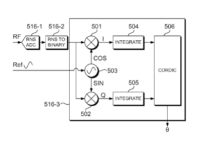
Referring now to Fig. 5, apparatus for measuring a phase angle is illustrated
according
to an embodiment of the present invention. The apparatus can be included in
the
calibrator of Fig. 1 for measuring a phase angle between a copy of the
reference signal
and the DAC 114 output signal to check whether the reference signal phase has
been
correctly preserved through the DSP 112. However, the invention is not limited
to this
application, and embodiments of the invention can be used in any application
where
phase angle measurement is required.
As shown in Fig. 5, the apparatus comprises a RNS ADC 516-1, a RNS-to-binary
converter 516-2 arranged to convert the RNS values output by the RNS ADC 516-1
to
conventional binary values, and a phase measurement module 516-3 which
receives the
digital output from the RNS ADC 516-1 and outputs a phase angle measurement 0.
In
other embodiments the RNS-to-binary converter 516-2 can be omitted, and the
phase
measurement module 516-3 can calculate the phase angle measurement directly
from
the RNS values output by the RNS ADC 516-1.
In the present embodiment, the phase measurement module 516-3 comprises first
and
second quadrature multipliers 5oi, 502 and a signal generator 503. The signal
CA 02924980 2016-03-17
WO 2015/044675
PCT/GB2014/052922
- 9 -
generator 503 is arranged to receive the reference signal (ref) supplied to
the DSP, and
generate sine and cosine quadrature reference signals at the frequency of the
reference
signal. The first and second quadrature multipliers 501, 502 are arranged to
multiply
the digital ADC output signal with the sine and cosine quadrature reference
signals to
generate in-phase (I) and quadrature (Q) signal components.
The phase measurement module 516-3 further comprises first and second
quadrature
integrators 504, 505 which are arranged to integrate the results of the
quadrature
multipliers 501, 502 in time. In the present embodiment, the quadrature
integrators
/0 504, 505 are arranged to perform integration over an integration period
chosen to be
an integer number of cycles of the reference frequency, which is the frequency
of the
reference signal (Ref). The effect of integrating over an integer number of
cycles of the
reference frequency is to reject most of the RF input signal content at
frequencies other
than the reference frequency, similar to a selective bandpass filtering
function. This
/5 has the advantage of effectively rejecting energy from the Hamming
interferer in bins
separate from the bin in which the integration peak falls, which is the bin
corresponding to the reference frequency.
The phase measurement module 516-3 further comprises a phase angle calculator
506
20 in the form of a Coordinate Rotation Digital Computer (CORDIC) block.
The CORDIC
506 is arranged to receive the integration results from the first and second
quadrature
integrators 504, 505 and calculate the inverse tangent function from the I and
Q
integration results, to give the phase angle measurement 0. Although in the
present
invention a CORDIC algorithm is used, embodiments of the present invention are
not
25 limited to the CORDIC implementation. The CORDIC algorithm is well-
known, and is
an efficient method of serially calculating the inverse tangent function.
However, other
algorithms may be used instead of CORDIC in other embodiments.
As described above, when a straight binary ADC is used the Hamming interferer
is
30 tightly coupled to the wanted tone, such that most of the energy from
the Hamming
interferer occurs at the same frequency as the wanted tone. This means that
the values
obtained by the integrators 504, 505 at the frequency bin for the wanted tone,
i.e. the
reference frequency, are significantly affected by the Hamming interferer.
However, in
embodiments of the present invention, the RNS ADC breaks up the spectral
35 relationship between the Hamming interferer and the wanted tone, with
the result that
the energy from the Hamming interferer is distributed across many frequency
bins.
CA 02924980 2016-03-17
WO 2015/044675 PCT/GB2014/052922
- 10 -
This energy is discarded during the integration stage, and the impact of the
Hamming
interferer on the value in the wanted frequency bin is correspondingly
reduced.
Although in the present embodiment, RNS-to-binary conversion is performed
before
performing quadrature conversion to obtain I and Q signal components, in other
embodiments RNS-to-binary conversion can be performed at a different point,
for
example between the quadrature multipliers 501, 502 and the integrators 504,
505.
Furthermore, although in the present embodiment the phase measurement module
/0 516-3 uses I/Q processing to measure the phase angle, in other
embodiments the phase
measurement module may obtain the phase angle through a different method. For
example, in an alternative embodiment the phase measurement module can be
arranged to analyse the digital samples from the RNS ADC by using a Fourier
transform, and to infer phase information relating to the analogue signal from
the
/5 complex coefficient of the relevant frequency bin. In this approach, the
reference signal
can be subjected to the same analysis, and the required phase angle can then
be derived
by computing the difference.
Referring now to Fig. 6, a method of measuring a phase angle is illustrated
according to
20 an embodiment of the present invention. First, in step S6oi, an analogue
signal is
sampled and converted to digital samples in the form of RNS values. The RNS
value for
each sample of the analogue signal is expressed as a set of residues. Step
S6oi
corresponds to the sampling and conversion function performed by a RNS ADC,
for
example the RNS ADC 516-1 of Fig. 5.
Next, in step S6o2 the digital samples are converted from RNS to a
conventional binary
coding scheme, for example straight binary, offset binary or two's complement.
Converting the RNS values to conventional binary values has the advantage that
standard binary arithmetic blocks such as adders and multipliers can be used.
Step
S6o2 corresponds to the conversion performed by the RNS-to-binary converter
516-2
of Fig. 5. Alternatively, in some embodiments step S6o2 can be omitted, and a
phase
angle can be calculated directly from the RNS values. Retaining the digital
samples as
RNS values can enable the phase angle measurement to be calculated faster,
since RNS
arithmetic is carry-free and can be performed in fewer steps than conventional
binary
arithmetic.
CA 02924980 2016-03-17
WO 2015/044675
PCT/GB2014/052922
- 11 -
Next, in step S6o3 a phase angle is measured from the digital samples. This
step can be
performed by a phase angle measurement module such as the one shown in Fig. 5.
However, as explained above, embodiments of the present invention are not
limited to
use of a CORDIC algorithm for calculating a phase angle, and in other
embodiments
different methods of calculating a phase angle can be used.
As described above, using a RNS ADC to perform analogue-to-digital conversion
in
phase measurement applications provides the advantage that the effect of the
Hamming interferer within the ADC is reduced, relative to other ADC designs.
Figures
7A, 7B, 8A and 8B graphically illustrate the improvement in the carrier-to-
interference
ratio (C/I), for a range of input signal powers, when a RNS ADC is used
instead of a
straight binary ADC.
Figure 7A plots the C/I in decibels (dB) against tone power in decibels
relative to full
/5 scale (dBFS) for a conventional 12-bit ADC (dashed line in Fig. 7A) and
for a RNS ADC
(solid line in Fig. 7A) using RNS [2, 3, 5, 11, 23], and Fig. 7B plots the
difference in C/I
between the 12-bit ADC and the RNS ADC. For most input signal powers, the RNS
ADC achieves an improvement of around 20 to 30 dB.
Investigations by the inventor have shown that the improvement is not limited
to the
12-bit example illustrated in Figs. 7A and 7B, and does not depend on a
particular
choice of RNS moduli. As a further example, Figs. 8A and 8B illustrate the
improvement in C/I ratio when a RNS [5, ii, 19] ADC (solid line in Fig. 8A) is
used
instead of a conventional 10-bit ADC (dashed line in Fig. 8A).
Whilst certain embodiments of the present invention have been described above,
the
skilled person will understand that many variations and modifications are
possible
without departing from the scope of the invention as defined in the
accompanying
claims.