Note: Descriptions are shown in the official language in which they were submitted.
CA 02925131 2016-03-22
WO 2015/051201 PCT/US2014/058946
SYSTEM AND METHOD FOR UNIFORM INTERLEAVING OF DATA ACROSS A
MULTIPLE-CHANNEL MEMORY ARCHITECTURE WITH ASYMMETRIC
STORAGE CAPACITY
DESCRIPTION OF THE RELATED ART
[0001] Computing devices are ubiquitous. These devices may include portable
computers, desktop computers and server computers and other devices of various
sizes.
In addition to the primary function of these devices, many include peripheral
functions.
For example, a cellular telephone may include the primary function of enabling
and
supporting cellular telephone calls and the peripheral functions of a still
camera, a video
camera, global positioning system (GPS) navigation, web browsing, sending and
receiving emails, sending and receiving text messages, push-to-talk
capabilities, etc. As
the functionality of such a device increases, the computing or processing
power required
and the data storage capacity to support such functionality also increases.
[0002] Some conventional computing device designs include multiple processors
and/or
processors with multiple cores to support the various primary and peripheral
functions
desired for a particular computing device. With the increased computing
capacity and
processor speed a number of techniques have been developed to minimize
bottlenecks
that can occur between the processors and/or processor cores and the system
memory.
One approach includes integrated circuit architectures that exchange data with
a random
access memory element twice in each clock cycle. For example, double data rate
(DDR)
random access memory (RAM) modules support these data exchanges. Even with
this
approach, today's systems with multiple processors and/or multiple cores
operate at
clock rates that exceed the data transfer rates of conventional memory
modules. Other
approaches include adding additional memory channels. A system that includes
two
memory channels can help to alleviate the problem by doubling the available
memory
bandwidth. The two channels are used simultaneously by a memory controller to
alleviate data transfer bottlenecks that can occur when writing data to and
reading data
from a RAM module.
[0003] When each memory channel communicates with a similarly constructed
(i.e.,
matched) memory module with equal storage capacity, not only can the
controller
transfer data to and from the memory space at the maximum data rate supported
by the
memory bus, the entire memory space is available to the memory controller to
place
application programs, or data files at any unused and desired location in the
memory
-1-
CA 02925131 2016-03-22
WO 2015/051201 PCT/US2014/058946
space. Thus, uniform interleaving or distribution of the data across the
available address
space is desired.
[0004] For conventional data interleaving schemes the storage capacity of the
memory
module(s) must be the same for the interleaver to access the memory modules at
the
maximum supported data transfer rate.This is generally not a problem as memory
module manufacturers provide integrated circuits with fixed storage
capacities. As long
as the manufacturer of the computing device deploys memory modules in pairs,
with
each pair having the same storage capacity, the storage capacity accessible by
each
memory channel is the same.
[0005] However, computing device manufacturers have communicated the desire to
provide a system memory capacity that is not a multiple of the minimum storage
capacity of a commercially available memory module. This makes it impossible
to use
commercially available memory modules and to arrange the same in a symmetric
capacity across two or more memory channels. For example, if a manufacturer
desires a
system memory capacity of 768 Mbytes and the smallest memory module capacity
available is 256 Mbytes, a manufacturer can achieve the total memory capacity
desired
by deploying three memory modules. However, only two of the three modules can
be
symmetrically arranged across separate memory channels.
[0006] Asymmetric memory capacities present an arrangement where a first
portion of
the total memory capacity can only be accessed in a non-interleaved manner at
a
reduced data rate than that of a second portion of the total memory capacity
that can be
accessed using a conventional interleaving function. Such an arrangement
introduces
complications on the operating system and/or application providers to identify
what
functions and applications can be sufficiently supported by a non-interleaved
(i.e.,
slower) data access.
[0007] Thus, there is a need for improved mechanisms for optimizing data
transfer rates
between memory channels that support asymmetric memory capacities.
SUMMARY OF THE DISCLOSURE
[0008] Systems and methods are disclosed that identify when a memory space
supported by a multiple channel memory architecture is populated with non-
uniform
data storage capacities across the multiple channels. In response, a number of
virtual
sectors of equal storage capacity are identified. Thereafter, an interleaving
function is
used to distribute data accesses to the memory space across the virtual
sectors.
-2-
CA 02925131 2016-03-22
WO 2015/051201 PCT/US2014/058946
[0009] An example embodiment includes a computing device with an interleaver
disposed in communication witha processor and a system memory. The interleaver
identifies locations in a memory space in the system memory. The memory space
is
supported by at least two physical channels and includes at least one memory
module
coupled to each of the physical channels. The memory space has a non-uniform
storage
capacity distributed across the physical channels. The interleaver is
responsive to logic
that identifies virtual sectors having a desired storage capacity. In
operation, the
interleaver accesses the asymmetric storage capacity uniformly across the
virtual sectors
in response to requests to access the memory space.
[0010] One example embodiment is a computing device that includes a mechanism
that
identifies when a memory space is arranged with a non-uniform storage capacity
across
a multiple-channel memory access architecture, further identifies a number of
virtual
sectors of desired storage capacity in the memory space, and applies an
interleaving
function that uniformly accesses the virtual sectors in response to requests
to access the
memory space.
[0011] Another example embodiment is a method for uniformly interleaving
memory
accesses across physical channels of a memory space with a non-uniform storage
capacity. The method includes the steps of identifying when a multiple-channel
memory architecture is provided an asymmetric storage capacity across the
multiple
channels, identifying a number of virtual sectors of equal capacity and
applying an
interleaving function via an interleaver that accesses the asymmetric storage
capacity
uniformly across the virtual sectors in response to requests to access the
memory space.
[0012] Another example embodiment is a non-transitory processor-readable
medium
having stored therein processor instructions and data that direct the
processor to: receive
an indication that a multiple-channel memory architecture is presently
populated with
memory modules that provide an asymmetric storage capacity across the multiple
channels, in response to the indication, identify a number of virtual sectors
of equal
capacity and apply an interleaving function that accesses the asymmetric
storage
capacity uniformly across the virtual sectors in response to requests to
access the
memory space.
BRIEF DESCRIPTION OF THE DRAWINGS
[0013] In the drawings, like reference numerals refer to like parts throughout
the
various views unless otherwise indicated. For reference numerals with letter
character
-3-
CA 02925131 2016-03-22
WO 2015/051201 PCT/US2014/058946
designations such as "102A" or "102B", the letter character designations may
differentiate two like parts or elements present in the same figure. Letter
character
designations for reference numerals may be omitted when it is intended that a
reference
numeral to encompass all parts having the same reference numeral in all
figures.
[0014] FIG. 1 is a schematic diagram illustrating an example embodiment of a
computing device.
[0015] FIG. 2 is schematic diagram illustrating an example embodiment of the
computing device of FIG. 1 with a symmetric memory capacity.
[0016] FIG. 3 is a schematic diagram illustrating the computing device of FIG.
2 with
an asymmetric system memory capacity.
[0017] FIG. 4is a schematic diagram of an example embodiment of the computing
device of FIG. 1 with a set of virtual sectors distributed in a 1:2 ratio
across two
physical channels.
[0018] FIG. 5 is a schematic diagram of an example embodiment of the computing
device of FIG. 1 with a set of virtual sectors distributed in a 1:2 ratio
across two
physical channels operated at different data transfer rates.
[0019] FIG. 6 is a schematic diagram of an example embodiment of the computing
device of FIG. 5 with a relatively larger set of virtual sectors distributed
in a 2:3 ratio
across two physical channels operated at different data transfer rates.
[0020] FIG. 7 is a schematic diagram of an example embodiment of a computing
device
with an alternative set of virtual sectors distributed in a 1:2:2:2 ratio
across 4 physical
channels operated at two different data transfer rates to achieve an
equivalent data
bandwidth of a symmetrically populated memory space.
[0021] FIG. 8 is a flowchart illustrating an example embodiment of a method
for
uniformly interleaving memory accesses across physical channels of a memory
space
with a non-uniform storage capacity.
DETAILED DESCRIPTION
[0022] The word "exemplary" is used herein to mean "serving as an example,
instance,
or illustration." Any aspect described herein as "exemplary" is not
necessarily to be
construed as preferred or advantageous over other aspects.
[0023] In this description, the term "application" may also include files
having
executable content, such as: object code, scripts, byte code, markup language
files, and
patches. In addition, an "application" referred to herein, may also include
files that are
-4-
CA 02925131 2016-03-22
WO 2015/051201 PCT/US2014/058946
not executable in nature, such as documents that may need to be opened or
other data
files that need to be accessed.
[0024] The term "content" may also include files having executable content,
such as:
object code, scripts, byte code, markup language files, and patches. In
addition,
"content"referred to herein, may also include files that are not executable in
nature, such
as documents that may need to be opened or other data files or data values
that need to
be accessed.
[0025] As used in this description, the terms "component," "database,"
"module,"
"system," and the like are intended to refer to a computer-related entity,
either
hardware, firmware, a combination of hardware and software, software, or
software in
execution. For example, a component may be, but is not limited to being, a
process
running on a processor, a processor, an object, an executable, a thread of
execution, a
program, and/or a computer. By way of illustration, both an application
running on a
computing device and the computing device may be a component. One or more
components may reside within a process and/or thread of execution, and a
component
may be localized on one computer and/or distributed between two or more
computers.
In addition, these components may execute from various computer-readable media
having various data structures stored thereon. The components may communicate
by
way of local and/or remote processes such as in accordance with a signal
having one or
more data packets (e.g., data from one component interacting with another
component
in a local system, distributed system, and/or across a network such as the
Internet with
other systems by way of the signal).
[0026] In this description, the term "portable computing device" ("PCD") is
used to
describe any device operating on a limited capacity rechargeable power source,
such as
a battery and/or capacitor. Although PCDs with rechargeable power sources have
been
in use for decades, technological advances in rechargeable batteries coupled
with the
advent of third generation ("3G") and fourth generation ("4G") wireless
technology
have enabled numerous PCDs with multiple capabilities. Therefore, a PCD may be
a
cellular telephone, a satellite telephone, a pager, a PDA, a smartphone, a
navigation
device, a smartbook or reader, a media player, a combination of the
aforementioned
devices, a laptop or tablet computer with a wireless connection, among others.
[0027] Interleaving functions can be adapted to support various configurations
of
memory modules deployed across multiple physical channels. A uniformly
interleaved
memory space will support memory accesses at a reduced data transfer rate than
the
-5-
CA 02925131 2016-03-22
WO 2015/051201 PCT/US2014/058946
data transfer rate otherwise possible when each physical channel is coupled to
the same
storage capacity.
[0028] Under certain conditions, the reduced data transfer rate or memory
access
bandwidth may be sufficient to meet or exceed desired system performance.
Otherwise,
when it is desired to achieve the memory access bandwidth that is possible
with a
uniform storage capacity across the multiple physical channels, an algorithmic
approach
is implemented in combination with the interleaving function to achieve an
equivalent
memory access bandwidth of a symmetrically arranged memory space.
[0029] When the memory space is populated with N (an integer) memory modules
having the same data storage capacity, a spreading function directs an
interleaver to
distribute the data across the virtual sectors. An example interleaving
function such as
the MOD function may be deployed in an interleaver. For example, to spread the
address A[7:0] over 3 channels to map a total of 192 memory words, where each
channel has 6-bit address ranges [5:0], mapping 64 memory words each, the
outcome of
A[7:0] MOD 3, can be used to select a channel. Hence, each channel will
receive
exactly a third of the 192 possible valid address patterns of A[7:0] in an
interleaved
manner. (Note that addresses 193 to 255 are invalid address patterns because
that
memory is unpopulated.) Then, a set of 5-bit intra-channel addressing
functions AO,
Al, A2 can be defined to select the memory locations within each channel.
Since the
subset of 64 memory locations of A[7:0] possible within each channel is known,
one
ordinarily skilled in the art using standard logic design and minimization
techniques can
design similar intra channel addressing functions that map these 64 addresses
to the 64
unique memory locations within each channel.
[0030] In another example, an interleaving function may be applied that
distributes data
across the virtual sectors over multiple conceptual rounds, though the actual
interleaving
function could be designed as a single stage using standard logic design and
minimization techniques. In an example arrangement with two memory modules
removed from a single channel of a 4-channel memory architecture, a desired
number of
bits / bytes are stored over the 3 populated channels in a round-robin fashion
over
multiple generations. A first portion of the bits/bytes are directed to a
specified storage
location in a memory module coupled to the first channel. A second portion of
the
bits/bytes to be stored are directed to a specified storage location in a
memory module
coupled to the second channel. A third portion of the bits/bytes to be stored
are directed
to a specified storage location in a memory module coupled to the third
channel. The
-6-
CA 02925131 2016-03-22
WO 2015/051201 PCT/US2014/058946
leftover bits/bytes that would otherwise be directed to a memory element
coupled to the
fourth channel when the fourth channel is coupled to memory modules can be
directed
to a specified storage location in a memory module coupled to the first
channel and so
on. Accordingly, the stored data is evenly spread across the available data
storage
capacity provided by memory modules coupled to 3 channels. The illustrated
embodiments include other example arrangements of a memory space having non-
uniform data storage capacities across multiple channels.
[0031] Although described with particular reference to operation within a PCD,
the
described memory management systems and methods are applicable to any
computing
system with a multiple channel memory architecture that is populated with a
non-
uniform data storage capacity across the respective channels. Stated another
way, the
memory management systems and methods are applicable to desktop computers,
server
computers or any electronic device with a non-uniformly distributed data
storage
capacity coupled to multiple physical channels.
[0032] Reference is now directed to the illustrated examples. Referring
initially to FIG.
1, an exemplary, non-limiting aspect of a portable computing device (PCD) is
shown
and is generally designated 100. As shown, the PCD 100 includes an on-chip
system
120 that includes a multicore CPU 210. The multicore CPU 210 includes a zeroth
core
215, a 1St or first core 216, and an Nth core 217.
[0033] As illustrated in FIG. 1, a display controller 128 and a touch screen
controller
130 are coupled to the multicore CPU 210. In turn, display/touchscreen 132,
external to
the on-chip system 120, is coupled to the display controller 128 and the touch
screen
controller 130.
[0034] FIG. 1 further indicates that a video encoder 134, e.g., a phase
alternating line
(PAL) encoder, a sequential couleur a memoire (SECAM) encoder, or a national
television system(s) committee (NTSC) encoder, is coupled to the multicore CPU
210.
Further, a video amplifier 136 is coupled to the video encoder 134 and the
display/touchscreen 132. Also, a video port 138 is coupled to the video
amplifier 136.
As depicted in FIG. 1, a universal serial bus (USB) controller 140 is coupled
to the
multicore CPU 210. Also, a USB port 142 is coupled to the USB controller 140.
A
system memory 230 and a subscriber identity module (SIM) card 146 may also be
coupled to the multicore CPU 210 with the connection 219 between the multicore
CPU
210 and the system memory 230 consisting of two or more physical channels or
paths
for transferring data between these elements of the on-chip system 120.
Further, as
-7-
CA 02925131 2016-03-22
WO 2015/051201 PCT/US2014/058946
shown in FIG. 1, a digital camera 148 may be coupled to the multicore CPU 210.
In an
exemplary aspect, the digital camera 148 is a charge-coupled device (CCD)
camera or a
complementary metal-oxide semiconductor (CMOS) camera.
[0035] As further illustrated in FIG. 1, a stereo audio CODEC 150 may be
coupled to
the multicore CPU 210. Moreover, an audio amplifier 152 may be coupled to the
stereo
audio CODEC 150. In an exemplary aspect, a first stereo speaker 154 and a
second
stereo speaker 156 are coupled to the audio amplifier 152. FIG. 1 shows that a
microphone amplifier 158 may be also coupled to the stereo audio CODEC 150.
Additionally, a microphone 116 may be coupled to the microphone amplifier 158.
In a
particular aspect, a frequency modulation (FM) radio tuner 162 may be coupled
to the
stereo audio CODEC 150. Also, a FM antenna 164 is coupled to the FM radio
tuner
162. Further, a stereo port 166 may be coupled to the stereo audio CODEC 150.
[0036] FIG. lalso indicates that a radio frequency (RF) transceiver 168 is
coupled to the
multicore CPU 210. An RF switch 170 may be coupled to the RF transceiver 168
and an
RF antenna 172. As shown in FIG. 1, a keypad 174 is coupled to the multicore
CPU
210. Also, a mono headset with a microphone 176 may be coupled to the
multicore
CPU 210. Further, a vibrator device 178 may be coupled to the multicore CPU
210.
FIG. lfurther shows that a power supply 180 may be coupled to the on-chip
system 120
via the USB controller 140. In a particular aspect, the power supply 180 is a
direct
current (DC) power supply that provides power to the various components of the
PCD
100 that require power. Further, in a particular aspect, the power supply is a
rechargeable DC battery or a DC power supply that is derived from an
alternating
current (AC) to DC transformer that is connected to an AC power source.
[0037] FIG. 1 further indicates that the PCD 100 may also include a network
card 188
that may be used to access a data network, e.g., a local area network, a
personal area
network, or any other network. The network card 188 may be a Bluetooth network
card,
a WiFi network card, a personal area network (PAN) card, or any other network
card
well known in the art. Further, the network card 188 may be incorporated in an
integrated circuit. That is, the network card 188 may be a full solution in a
chip, and
may not be a separate network card 188.
[0038] As depicted in FIG. 1, the display/touchscreen 132, the video port 138,
the USB
port 142, the camera 148, the first stereo speaker 154, the second stereo
speaker 156, the
microphone 116, the FM antenna 164, the stereo port 166, the RF switch 170,
the RF
-8-
CA 02925131 2016-03-22
WO 2015/051201 PCT/US2014/058946
antenna 172, the keypad 174, the mono headset 176, the vibrator 178, and the
power
supply 180 are external to the on-chip system 120.
[0039] RF transceiver 168, which may include one or more modems, may support
one
or more of global system for mobile communications ("GSM"), code division
multiple
access ("CDMA"), wideband code division multiple access ("W-CDMA"), time
division synchronous code division multiple access ("TDSCDMA"), long term
evolution ("LTE"), and variations of LTE such as, but not limited to, FDB/LTE
and
PDD/LTE wireless protocols.
[0040] In the illustrated embodiment, a single instance of a multi-core CPU
210 is
depicted. However, it should be understood that any number of similarly
configured
multi-core CPUs can be included to support the various peripheral devices and
functions
associated with the PCD 100. Alternatively, a single processor or multiple
processors
each having a single arithmetic logic unit or core could be deployed in a PCD
or other
computing devices to support the various peripheral devices and functions
associated
with the PCD 100 as may be desired.
[0041] The illustrated embodiment shows a system memory 230 that is arranged
within
a fully integrated on-chip system 120. However, it should be understood that
two or
more vendor provided memory modules having a corresponding data storage
capacity of
M bytes may be arranged external to the on-chip system 120. When arranged
external to
the on-chip system 120, the various memory modules supporting the system
memory
230 are coupled to the CPU 210 by way of a modified multiple channel memory
bus
(not shown) including suitable electrical connections for transferring data
and power to
the memory modules.
[0042] In a particular aspect, one or more of the method steps described
herein may be
enabled via a combination of data and processor instructions stored in the
system
memory 230. These instructions may be executed by the multicore CPU 210 in
order to
perform the methods described herein. Further, the multicore CPU 210, the
memory
230, an EEPROM (not shown) or a combination thereof may serve as a means for
storing a non-transitory representation of memory management logic, including
interleaver logic, and configuration parameters for executing one or more of
the method
steps described herein. As indicated, a memory controller or other memory
management
logic identifies when the system memory 230 is populated in an asymmetric
manner
with respect to multiple memory access channels that communicate data between
the
CPU 210 and the system memory 230. As also indicated, interleaver logic
responds in
-9-
CA 02925131 2016-03-22
WO 2015/051201 PCT/US2014/058946
accordance with the physical architecture supporting the system memory 230 by
defining virtual sectors having equal storage capacity and in response to
requests to
access the memory space, applying an algorithmic solution to distribute data
uniformly
across the virtual sectors.
[0043] FIG. 2 is schematic diagram illustrating details of the CPU 210, the
system
memory 230 and the connection 219 that enables data transfers between the CPU
210
and the memory space 290 when the memory space 290 is supported with a
symmetric
memory capacity across two physical channels. As indicated in FIG. 2, the
memory
space 290 is supported by a first set of two memory modules coupled to the CPU
210
via channel 220 (channel 0) and a second set of two memory modules coupled to
the
CPU 210 via channel 222 (channel 1). The first set of memory modules includes
memory module 291 and memory module 292. The memory module 291 and the
memory module 292, which may be implemented with dynamic random access memory
(DRAM) integrated circuits, each provide a data storage capacity of M bytes.
The
second set of memory modules includes memory module 293 and memory module 294.
The memory module 293 and the memory module 294, which may be implemented
with DRAM integrated circuits,also provide a data storage capacity of M bytes.
With
each of the memory modules 291-294 including the same circuit architecture and
having
the same capacity of M bytes, the 0/S logic 213 can use the memory controller
211 to
place data to be stored to any desired location across the memory space 290.
Not only
can the data stored therein be placed as desired by the memory controller 211,
the data
can be transferred to the memory space 290 of 4M bytes at the maximum
bandwidth and
with a uniform latency.
[0044] As indicated in FIG. 2, the CPU 210 includes a memory controller 211,
interleaver logic 212, operating system (0/S) logic 213, cache 214 and core
215. These
elements are coupled to each other along one or more internal connections or
data buses
(not shown) within the CPU 210. The memory controller 211 is a digital circuit
which
manages the flow of data going to and from the system memory 230.The memory
controller 211 is assisted or augmented by the interleaver logic 212. The
interleaver
logic 212 provides an address, label or other information that identifies
which of the
available channels is to be used for a particular I/O operation between the
CPU 210 and
the system memory 230. The interleaver logic typically also rearranges or
recomputes
the sub-channel address being sent to each channel, in a manner that is
compatible with
the interleaving function. (For example, a trivial two-channel interleaver for
a system
-10-
CA 02925131 2016-03-22
WO 2015/051201 PCT/US2014/058946
with a 32-bit address A[31:0] might use address bit A[10] to select the
channel, and then
generate intra-channel addresses A0[A[31:11],A[9:0]] and Al [31:11],A[9:0]]
for
channels 0 and 1, respectively.) The 0/S logic 213 includes a set of
instructions that
when executed by the core 215 manages the various peripheral resources and
provides
common services for computer programs stored in the memory space 290.The 0/S/
logic 213 can be stored in the system memory 230 and read into the CPU 210 as
required. Alternatively, the 0/S logic 213 can be stored in a read-only memory
module
coupled to or integrated in the CPU 210. The cache 214 is a smaller, faster
memory
used by the CPU 210 to store copies of the data from frequently used system
memory
locations. The cache 214 reduces the average time to access memory. As long as
some
memory accesses are from cached memory locations, the average latency of
memory
accesses will be closer to the cache latency than to the latency of system
memory 230.
The core 215 includes a set of circuits that read, buffer and execute program
instructions.
[0045] In the illustrated arrangement, the memory controller 211 is integrated
on the
same die as the CPU 210. In alternative arrangements, the memory controller
211 can
be implemented on a separate integrated circuit in communication with the CPU
210.
The memory controller 211 is arranged with a front-end portion and a back-end
portion.
The front-end portion buffers requests and responses and provides an interface
to the
CPU 210 and other portions of the computing device 200 (not shown). This front-
end
portion is generally independent of the memory module type. In contrast, the
back-end
portion provides an interface to the memory modules and is dependent on the
type of
memory circuit in the memory modules.
[0046] In the illustrated arrangement, the interleaver logic 212 is integrated
on the same
die and depicted as a separate circuit or set of circuits as the core 215 and
the memory
controller 211. In alternative embodiments, the interleaver logic 212 may be a
sub-part
of the circuits that enable one of the memory controller 211 or the 0/S logic
213.
However embodied, the interleaver logic 212 when presented with a full
complement or
at least a balanced complement of addressable memory modules uses the channel
220
and the channel 222 to uniformly distribute data to be stored in the memory
space 290.
[0047] FIG. 3 is a schematic diagram illustrating the computing device of FIG.
2 with
an asymmetric system memory capacity.An asymmetric system memory capacity
occurs when the manufacturer elects to provide less than a full complement of
memory
modules or when a memory module fails. As indicated in the example embodiment
-11-
CA 02925131 2016-03-22
WO 2015/051201 PCT/US2014/058946
illustrated in FIG. 3, the memory space 390 is supported by a first memory
module 391
coupled to the CPU 210 via channel 220 (channel 0) and two memory modules
coupled
to the CPU 210 via channel 222 (channel 1). The memory module 391, memory
module 393, and the memory module 394 may be implemented with DRAM integrated
circuits each having a data storage capacity of M bytes. With each of the
memory
modules 291, 293, 294 including the same circuit architecture and having the
same
capacity of M bytes,the channel 220 (channel 0) is coupled to M bytes whereas
the
channel 222 (channel 1) is coupled to 2M bytes. As indicated in FIG. 3 there
is a 1:1
data access ratio between the physical channels 220, 222 across the memory
module
391 and the memory module 393. The absence of a second memory module coupled
to
the channel 220 results in a 0:1 data access ratio between the physical
channels 220,
222. That portion of the memory space 390 supported by the memory module 394
is
incapable of receiving interleaved data and thus processes less data per unit
time than
that portion of the memory space where two memory modules can be accessed
simultaneously via respective channels. The absence of the second memory
module
coupled to the channel 220 may be detectable by the memory controller 211,
which may
communicate a signal indicating the same to the interleaver logic 212 or other
logic
accessible to the CPU 210. In response, the interleaver logic 212 or other
logic may
respond in a pre-programmed manner based on one or more system parameters.
Alternatively, the computing device 300 may respond in a fixed manner.
[0048] A multiple-channel memory access architecture 302 arranged with an
asymmetric storage capacity across the physical channels 220, 222 can be made
operational by a partial or non-uniform interleaving function. That is, a
first portion of
the memory space 390 (the lowermost portion in the illustrated embodiment) can
be
interleaved at the maximum data rate supported by the memory module 391 and
the
memory module 393, while a second portion of the memory space 390 can only
process
non-interleaved memory access requests. Thus, the interleaver logic 212 is
used to
transfer data to and from the memory space over 2M bytes of the total 3M
storage
capacity.
[0049] While supportable, such an arrangement introduces a significant burden
on the
0/S logic 213 and/or application programs (not shown) that use services
provided by
the 0/S logic 213 under circumstances where not all memory accesses can be
sufficiently supported at the non-interleaved data transfer rate. When this is
the case, it
is incumbent on the 0/S logic 213 and/or application programs to identify
which
-12-
CA 02925131 2016-03-22
WO 2015/051201 PCT/US2014/058946
memory accesses can be addressed to the non-interleaved portion of the memory
space
390. Alternatively, the computing device 300 could send all memory I/O at the
non-
interleaved or slower data transfer rate.
[0050] FIG. 4 is a schematic diagram of an example embodiment of the computing
device of FIG. 1 with a set of virtual sectors distributed in a 1:2 ratio
across two
physical channels.As indicated in the example embodiment illustrated in FIG.
4, the
memory space 440 is supported by a first memory module 441 coupled to the CPU
210
via channel 220 (channel 0) and two memory modules coupled to the CPU 210 via
channel 222 (channel 1). The memory module 441, memory module 443, and the
memory module 444 may be implemented with DRAM integrated circuits each having
a
data storage capacity of M bytes. With each of the memory modules 441, 443,
444
including the same circuit architecture and having the same capacity of M
bytes, the
channel 220 (channel 0) is coupled to M bytes whereas the channel 222 (channel
1) is
coupled to 2M bytes. However, instead of using a partial interleave function
to
interleave data across two of the three available memory modules, the memory
space
440 is divided into virtual sectors of equal capacity. As shown in FIG. 4 a
virtual sector
coincides with each of the memory module 441, memory module 443 and memory
module 444. As indicated in FIG. 4 there is a 1:2 data access ratio between
the physical
channels 220.
[0051] The multiple-channel memory access architecture with an asymmetric
storage
capacity, as presented in FIG. 4, uses a virtual interleave function enabled
by the
modified interleaver logic 418. When the number of virtual sectors is odd, the
modified
interleaver logic 418 uses an odd-way spreading function to distribute data
across the
virtual sectors.
[0052] The electronically erasable programmable read only module (EEPROM) 411
is
integrated with the processor CPU 210 to provide storage for programmable
parameters
and desired spreading functions to direct or adjust the modified interleaver
logic 418
when distributing the data across the virtual channels.For example, a 3-way
spreading
function dynamically distributes memory access in a 1:2 ratio between channel
220 and
channel 222 across the memory space 440. Consequently, the available capacity
of the
memory space 440 can be uniformly interleaved. In such arrangements, the rate
of data
transfers between the CPU 210 and the memory space 440 over the memory space
440
will be reduced from the maximum data transfer rate supported by matched
memory
modules across both channels but is faster and easier to manage than the
slower non-
-13-
CA 02925131 2016-03-22
WO 2015/051201 PCT/US2014/058946
interleaved data transfer supported by the partial interleaving method
illustrated in FIG.
3.Since all memory accesses are performed at the same data transfer rate, the
0/S logic
216 and or application programs executing in the core 215 can place data
anywhere in
the memory space 440.
[0053] In alternative embodiments, the virtual sector interleaving function
may be
programmed or adjusted to use more or fewer virtual sectors. In some
arrangements,
the number of virtual sectors used by the modified interleaver logic 418 may
be less
than the number of memory modules supporting the memory space 440. In some
other
arrangements, the number of virtual sectors used by the modified interleaver
logic 418
may be more than the number of memory modules supporting the memory space 440.
Such mismatches between the number of memory modules and the number of virtual
sectors may ease the complexity of evenly dividing the available storage
capacity into
virtual sectors when memory modules having a different capacity are used to
the
support the memory space. A programmable virtual sector spreading function
that
distributes data across multiple channels allows the same CPU 210 to support
both fully
populated and partially populated memory channels.
[0054] An example spreading function may include a code for defining a memory
access channel. For systems with three available channels an example spreading
function such as the MOD function may be deployed. For example, to spread the
address A[7:0] over 3 channels to map a total of 192 memory words, where each
channel has 6-bit address ranges [5:0], mapping 64 memory words each, the
outcome of
A[7:0] MOD 3, can be used to select a channel. Hence, each channel will
receive
exactly a third of the 192 possible valid address patterns of A[7:0] in an
interleaved
manner. (Note that addresses 193 to 255 are invalid address patterns because
that
memory is unpopulated.) Then, a set of 5-bit intra-channel addressing
functions AO,
Al, A2 can be defined to select the memory locations within each channel.
Since the
subset of 64 memory locations of A[7:0] possible within each channel is known,
one
ordinarily skilled in the art using standard logic design and minimization
techniques can
design intra channel addressing functions of his liking that map these 64
addresses to
the 64 unique memory locations within each channel.
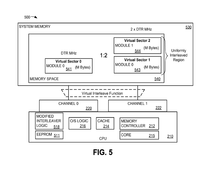
[0055] FIG. 5 is a schematic diagram of an example embodiment of the computing
device of FIG. 1 with a set of virtual sectors distributed in a 1:2 ratio
across two
physical channels operated at different data transfer rates .As indicated in
the example
embodiment illustrated in FIG. 5, the memory space 540 is supported by a first
memory
-14-
CA 02925131 2016-03-22
WO 2015/051201 PCT/US2014/058946
module 541 coupled to the CPU 210 via channel 220 (channel 0) and two memory
modules coupled to the CPU 210 via channel 222 (channel 1). The memory module
541, memory module 543, and the memory module 544 may be implemented with
DRAM integrated circuits each having a data storage capacity of M bytes. With
each of
the memory modules 541, 543, 544 including the same circuit architecture and
having
the same capacity of M bytes, the channel 220 (channel 0) is coupled to M
bytes
whereas the channel 222 (channel 1) is coupled to 2M bytes. However, instead
of using
a virtual interleave function to interleave data across three virtual sectors
alone, as
shown in FIG. 4, the memory space 540 is divided into virtual sectors of equal
capacity
and the modified interleaver logic 518 uses a first data transfer rate when
communicating over channel 220 and a second data transfer rate when
communicating
over channel 222. In an example embodiment, the memory module 541 is a low-
power
double data rate 2 (LPDDR2) memory element with a data capacity of 256 MBytes
and
capable of operating at a clock frequency of 266 MHz. In this same example,
the
memory module 543 and the memory module 544 arc LPDDR2 memory elements with
the same data capacity but are capable of operating at a clock frequency of
533 MHz.
Consequently, the example embodiment achieves a uniform bandwidth across the
memory space 540 while allowing for potential cost savings associated with the
asymmetric data storage capacity across the physical channels. While the
example
embodiment includes a 1:2 capacity ratio across the channels, a 1:2 ratio in
the virtual
sectors distributed about the channels and a 1:2 ratio in clock frequencies,
the clock
frequencies are independent of the virtual sector ratio and the number of
virtual sectors
coupled to each channel.
[0056] As shown in FIG. 5, a virtual sector coincides with each of the memory
module
541, memory module 543 and memory module 544. As further indicated in FIG. 5
there is a 1:2 data access ratio between the physical channels 220, 222. In
addition, the
memory modules 543, 544 in communication with channel 222 define a region of
the
memory space 540 where the modified interleaver logic 518 can uniformly
interleave
data at the highest rate supported by the memory modules (or a maximum data
transfer
rate) and the channel or a desired data transfer rate that is slower than the
maximum
data transfer rate. In the illustrated embodiment, channel 222 communicates
data with
the CPU 210 at a data transfer rate that is twice the data transfer rate
supported by
channel 220.
-15-
CA 02925131 2016-03-22
WO 2015/051201 PCT/US2014/058946
[0057] The EEPROM511 is integrated with the processor CPU 210 to provide
storage
for programmable parameters and desired spreading functions to direct or
adjust the
modified interleaver logic 518 when distributing the data across the virtual
channels. In
some arrangements the EEPROM 511 will include one or more parameters that
identify
the number of virtual sectors, the number of physical communication channels,
and the
data transfer rates to use when spreading data across the memory space 540. In
some
arrangements, the data transfer rates used to communicate data across the
channels
between the CPU 210 and the memory space 540 may be identified as functions of
the
other channel or channels.
[0058] FIG. 6 is a schematic diagram of an example embodiment of the computing
device of FIG. 5 with a relatively larger set of virtual sectors distributed
in a 2:3 ratio
across two physical channels operated at different data transfer rates.As
indicated in the
example embodiment illustrated in FIG. 6, the memory space 640 is supported by
a
memory module 641 and a memory module 642 coupled to the CPU 210 via channel
220 (channel 0) and memory module 644, memory module 645 and memory module
646 coupled to the CPU 210 via channel 222 (channel 1). The memory modules641,
642, 644, 645, 646 may be implemented with DRAM integrated circuits each
having a
data storage capacity of M bytes. With each of the memory modules 641, 642,
644,
645, 646 including the same circuit architecture and having the same capacity
of M
bytes, the channel 220 (channel 0) is coupled to 2M bytes of storage capacity
whereas
the channel 222 (channel 1) is coupled to 3M bytes of storage capacity. Here,
the
memory space 640 is divided into five virtual sectors of equal capacity and
the modified
interle aver logic 618 uses a first data transfer rate when communicating over
channel
220 and a second data transfer rate when communicating over channel 222.
[0059] As indicated in FIG. 6, the first and second data transfer rates
(f(0),f(1)) can be
determined as a function of a data transfer rate deployed in a fully
interleaved system, ft,
the number of virtual sectors in the channel (No, N1) and the ratio of the
number of
physical channels to the total number of virtual sectors (P/Vtot) in the
memory space
640. Specifically, first and second data transfer rates that permit the memory
space 640
to achieve the bandwidth provided by a matched capacity fully-interleaved
storage
system can be determined by the product of the data transfer frequency of the
fully
interleaved system, the number of virtual sectors in the channel and the ratio
of the
number of physical channels to the total number of virtual sectors deployed by
the
system 600.
-16-
CA 02925131 2016-03-22
WO 2015/051201 PCT/US2014/058946
[0060] In an example embodiment, the memory module 641 and the memory module
642 are DRAM elementseach with a data capacity of 256 MBytes and capable of
operating at a clock frequency of 320MHz. In this same example, the memory
module
644, memory module 645 and the memory module 646 are DRAM elements with the
same data capacity of 256 Mbytes but capable of operating at a clock frequency
of
480MHz. Consequently, the example embodiment achieves a uniform bandwidth
across the memory space 640 while allowing for potential cost savings
associated with
the asymmetric data storage capacity across the physical channels. While the
example
embodiment includes a 2:3 capacity ratio across the channels, a 2:3 ratio in
the virtual
sectors distributed about the channels and a 2:3 ratio in clock frequencies,
the clock
frequencies are independent of the virtual sector ratio and the number of
virtual sectors
coupled to each channel.
[0061] As shown in FIG. 6, a virtual sector coincides with each of the memory
modules641, 642, 644, 645, 646. In addition, the memory modules 644-646 in
communication with channel 222 define a region of the memory space 640 where
the
modified interleaver logic 618 can uniformly interleave data at the highest
rate
supported by the memory modules and the channel or a desired data transfer
rate that is
slower than the maximum data transfer rate. In the illustrated embodiment,
channel 222
communicates data with the CPU 210 at a data transfer rate that is one and
half times
the data transfer rate supported by channel 220.
[0062] The EEPROM 611 is integrated with the processor CPU 210 to provide
storage
for programmable parameters and desired spreading functions to direct or
adjust the
modified interleaver logic 618 when distributing the data across the virtual
channels. In
some arrangements the EEPROM 611 will include one or more parameters that
identify
the number of virtual sectors, the number of physical communication channels,
and the
data transfer rates to use when spreading data across the memory space 640. In
some
arrangements, the data transfer rates used to communicate data across the
channels
between the CPU 210 and the memory space 640 may be identified as functions of
the
other channel or channels.
[0063] FIG. 7 is a schematic diagram of an example embodiment of a computing
device
with an alternative set of virtual sectors distributed in a 1:2:2:2 ratio
across 4 physical
channels operated at two different data transfer rates to achieve an
equivalent data
bandwidth of a symmetrically populated memory space.As indicated in the
example
embodiment illustrated in FIG. 7, the memory space 740 is supported by a
memory
-17-
CA 02925131 2016-03-22
WO 2015/051201 PCT/US2014/058946
module 741 coupled to the CPU 210 via channel 220 (channel 0), amemory module
743
and a memory module 744 coupled to the CPU 210 via channel 222 (channel 1), a
memory module 745 and a memory module 746 coupled to the CPU 210 via channel
224 (channel 2), a memory module 747 and a memory module 748 coupled to the
CPU
210 via channel 226 (channel 3). The memory modules741, 743, 744, 745, 746,
747,
748 may be implemented with DRAM integrated circuits each having a data
storage
capacity of M bytes. With each of the memory modules 741, 743-748 including
the
same circuit architecture and having the same capacity of M bytes, the channel
220
(channel 0) is coupled to M bytes of storage capacity whereas the channels
222, 224,
226 (Channels 1-3) are coupled to 2M bytes of storage capacity. Here, the
memory
space 740 is divided into seven virtual sectors of equal capacity and the
modified
interleaver logic 718 uses a first data transfer rate when communicating over
channel
220 and a second data transfer rate when communicating over channels 222, 224,
226.
[0064] As indicated in FIG. 7, first and second data transfer rates (f(0),
f(1, 2, 3)) can be
determined as a function of a data transfer rate deployed in a fully
interleaved system, ft,
the number of virtual sectors in the channel (No, N1,2,3) and the ratio of the
number of
physical channels to the total number of virtual sectors (P/V0) in the memory
space
740. Specifically, first and second data transfer rates that permit the memory
space 740
to achieve the bandwidth provided by a matched capacity fully-interleaved
storage
system can be determined by the product of the data transfer frequency of the
fully
interleaved system, the number of virtual sectors in the channel and the ratio
of the
number of physical channels to the total number of virtual sectors deployed by
the
system 700.
[0065] In an example embodiment, the memory module 741 is a DRAM element with
a
data capacity of 256 MBytes and capable of operating at a clock frequency of
about
229MHz. In this same example, the memory modules743-748 are DRAM elements
with the same data capacity of 256 Mbytes but capable of operating at a clock
frequency
of about 457MHz. Consequently, the example embodiment achieves a uniform
bandwidth across the memory space 740 while allowing for potential cost
savings
associated with the asymmetric data storage capacity across the four physical
channels.
While the example embodiment includes a 1:2:2:2 capacity ratio across the four
channels, a 1:2:2:2 ratio in the virtual sectors distributed about the
channels and about a
1:2 ratio in clock frequencies, the clock frequencies may be applied
independent of the
virtual sector ratio and the number of virtual sectors coupled to each
channel.
-18-
CA 02925131 2016-03-22
WO 2015/051201 PCT/US2014/058946
[0066] As shown in FIG. 7, a virtual sector coincides with each of the memory
modules
741, 743-748. In addition, the memory modules 743-748 in communication with
channels 222, 224, 226 define a region of the memory space 740 where the
modified
interleaver logic 718 can uniformly interleave data at the highest rate
supported by the
memory modules and the channel or a desired data transfer rate that is slower
than the
maximum data transfer rate. In the illustrated embodiment, each of channels
222, 224,
226 communicates data with the CPU 210 at a data transfer rate that is about
twice the
data transfer rate supported by channel 220.
[0067] The EEPROM 711 is integrated with the processor CPU 210 to provide
storage
for programmable parameters and desired spreading functions to direct or
adjust the
modified interleaver logic 718 when distributing the data across the virtual
channels. In
some arrangements the EEPROM 711 will include one or more parameters that
identify
the number of virtual sectors (e.g., seven), the number of physical
communication
channels (e.g., 4), and the data transfer rates (229 MHz, 457 MHz) to use when
spreading data across the memory space 740.
[0068] While the illustrated embodiments include an even number of channels
and an
odd number of virtual sectors distributed over an odd number of memory
modules,
many other arrangements are possible that result in an asymmetric memory
capacity
across multiple channels. For example, an even number of memory modules can be
deployed across an odd number of channels. In one such arrangement, 4 total
memory
modules may be distributed across three channels (1:1:2, 1:2:1, or 2:1:1).
When the
memory modules share the same storage capacity, the number of virtual sectors
may be
equal to or less than the storage capacity of the memory modules. By way of
further
example, asymmetry in storage capacity across channels can be the result of
deploying
memory modules having different storage capacities across an even number of
channels.
In one such arrangement, a first memory module having a storage capacity of
1GB is
coupled to a first channel and a second memory module having a storage
capacity of
2GB is coupled to a second channel. In this arrangement, the interleaver
function may
respond by distributing the data equally across three virtual sectors of 1 GB
each. These
and other arrangements with asymmetric storage capacities distributed across
multiple
channels can be improved by the described interleaving functions and other
functions
that take advantage of using virtual sectors to access the available storage
in a
computing device.
-19-
CA 02925131 2016-03-22
WO 2015/051201 PCT/US2014/058946
[0069] FIG. 8 is a flowchart illustrating an example embodiment of a method
800 for
uniformly interleaving memory accesses across physical channels of a memory
space
with a non-uniform storage capacity. In block 802, a memory controller or
other sensor
associated with a computing system identifies when a memory space includes a
non-
uniform data storage capacity across multiple physical channels between a CPU
210 and
a system memory. In block 804, a programmable interleaver or interleaver logic
identify a set of virtual sectors of a desired storage capacity in the memory
space. In
block 806, the interleaver or interleaver logic responds to requests to access
the memory
space in a uniform manner across the virtual sectors or a portion of the
virtual sectors in
the memory space. In decision block 808, a determination is made to continue
to
process requests to access the memory space using the interleaver or
interleaver logic.
When the response is affirmative as indicated by the flow control arrow
labeled "Yes,"
the functions in block 806 and 808 are repeated. Otherwise, as indicated by
the flow
control arrow labeled "No" exiting decision block 808 the method 800
terminates.
[0070] Certain steps in the processes or process flows described in this
specification
naturally precede others for the invention to function as described. However,
the
invention is not limited to the order of the steps described if such order or
sequence does
not alter the functionality of the invention. That is, it is recognized that
some steps may
performed before, after, or in parallel (substantially simultaneously) with
other steps
without departing from the scope of the invention. In some instances, certain
steps may
be omitted or not performed without departing from the invention. Further,
words such
as "thereafter", "then", "next", "subsequently", etc. are not intended to
limit the order of
the steps. These words are simply used to guide the reader through the
description of the
exemplary method.
[0071] Additionally, one of ordinary skill in programming is able to write
computer
code or identify appropriate hardware and/or circuits to implement the
disclosed
invention without difficulty based on the flow charts and associated
description in this
specification, for example. Therefore, disclosure of a particular set of
program code
instructions or detailed hardware devices is not considered necessary for an
adequate
understanding of how to make and use the invention. The inventive
functionality of the
claimed processor-enabled processes is explained in more detail in the above
description
and in conjunction with the drawings, which may illustrate various process
flows.
[0072] In one or more exemplary aspects as indicated above, the functions
described may be implemented in hardware, software, firmware, or any
combination
-20-
CA 02925131 2016-03-22
WO 2015/051201 PCT/US2014/058946
thereof. If implemented in software, the functions may be stored as one or
more
instructions or code on a computer-readable medium, such as a non-transitory
processor-readable medium. Computer-readable media include data storage media.
[0073] A storage media may be any available media that may be accessed by a
computer or a processor. By way of example, and not limitation, such computer-
readable media may comprise RAM, ROM, EEPROM, CD-ROM or other optical disk
storage, magnetic disk storage or other magnetic storage devices, or any other
medium
that may be used to carry or store desired program code in the form of
instructions or
data structures and that may be accessed by a computer. Disk and disc, as used
herein,
includes compact disc ("CD"), laser disc, optical disc, digital versatile disc
("DVD"),
floppy disk and blu-ray disc where disks usually reproduce data magnetically,
while
discs reproduce data optically with lasers. Combinations of the above should
also be
included within the scope of non-transitory computer-readable media.
[0074] Although selected aspects have been illustrated and described in
detail, it will be
understood that various substitutions and alterations may be made herein
without
departing from the present systems and methods, as defined by the following
claims.
-21-