Note: Descriptions are shown in the official language in which they were submitted.
CA 02925248 2016-03-29
276985
OPTICAL CURRENT TRANSDUCER WITH OFFSET CANCELLATION AND
CURRENT LINEARIZATION
FIELD OF THE INVENTION
[0001] The present disclosure generally relates to optical current
transducers. More
particularly, the present disclosure relates to optical current transducers
with offset
cancellation.
BACKGROUND OF THE INVENTION
[0002] High voltage transmission lines require permanent current or voltage
monitoring in order to mitigate faults. Specifically, the ability to quickly
and reliably detect
current transients is paramount because protection circuits must react in
adequate time to
isolate or remove short circuits that can damage equipment located at either
end of a
transmission line.
[0003] In some applications, large current transients can be measured using
traditional
iron core current transformers. Such transformers include costly ceramic
insulators that are
used to provide adequate isolation between the transformers' windings. As
such, iron core
transformers may not be an economical solution when considering deployment in
large
electricity distribution networks. Most importantly, however, these
transformers have
undesired performance characteristics. Namely, they can introduce significant
distortions
in the measured current signal due to the hysteresis of their iron cores.
[0004] Fiber-optic current transducers (FOCTs) have been used as an
alternative
technology to circumvent the aforementioned issues; FOCTs are less costly
(when applied
to high-voltage lines), and they have superior performance. They operate on
the principle
of Faraday rotation, which is a magneto-optical effect whereby a rotation of
the plane of
polarization of a light beam confined in a fiber-optic waveguide placed near
the
transmission line is observed in response to a magnetic field induced by the
occurrence of
the large current transient. The rotation angle is linearly proportional to
the component of
1
CA 02925248 2016-03-29
276985
the magnetic field in the direction of propagation of the light, and as such,
the change in
angle can be correlated with the strength of the magnetic field, which can in
turn be used
to calculate the current.
[0005] A typical reflection-based FOCT measurement system includes a module
of
optical components with three fibers attached thereto. Two of the fibers (data
fibers) are
connected to a receiver, and the third fiber is a low birefringence fiber
(LBF) that is
wrapped around the transmission line or conductor.
[0006] Inside the module, there is a polarizer that polarizes the light at
zero degrees.
After the light is polarized, it is rotated by 22.5 degrees using a Faraday
rotator. From the
rotator, the light enters the LBF wherein it is further rotated by the
magnetic field induced
by the current in the transmission line. At the end of the LBF, there is a
mirror that reflects
the light back to the rotator, which rotates the light another 22.5 degrees.
After the second
rotation, the light is broken into two components that are transduced by the
receiver into
two electrical signals denoted "X" and "Y."
[0007] The Faraday rotator may cause significant errors in the X and Y
components.
These errors are manifested as DC offsets in each of the signals, and they are
due to
variations in temperature at the crystal that make up the Faraday rotator. As
such, these
offsets are termed "crystal offsets." Offsets may also arise from losses that
occur when
light travels through the data fibers. All of these offsets can introduce
significant errors in
estimating the current in the transmission line.
[0008] Furthermore, in typical FOCTs, at large current regimes (i.e. at
currents greater
than 4,000 A (rms)), the measured current typically exhibits'a high degree of
non-linearity,
which leads to inaccurate estimations of the current in the transmission line.
Furthermore,
typical FOCTs cannot track sudden changes that occur in the current in the
transmission
line because they make use of slow analog components to process the X and Y
signals. As
such, conventional FOCTs also produce erroneous measurements in these
situations.
2
CA 02925248 2016-03-29
276985
SUMMARY
[0009] FOCTs configured according to embodiments of the present disclosure
have
several advantages that help mitigate several shortcomings known in the
relevant art(s).
For example, embodiments of the present disclosure allow offsets due to
temperature
variations to be removed from the measured signal and thus provide a more
accurate output
than what is possible with conventional FOCTs. Furthermore, FOCTs configured
according to the teachings featured herein have the advantage of removing non-
symmetrical features in the measured current waveform, thus making it possible
to provide
accurate information when processing the current using Fourier Transform
techniques, for
example. Specifically, FOCTs configured according to the present embodiments
can
linearize the measured current waveform, thus making it possible to measure
currents up
to the maximum current rating of the LBF (i.e. currents up to 35,000 A (rms))
with a high
degree of fidelity. These advantages, and others that will be readily apparent
to one of skill
in the relevant art(s), are provided by the novel embodiments disclosed
herein.
[0010] In one embodiment, the present disclosure features a system for use
with a fiber-
optic current transducer. The system includes a processing unit configured to
transduce a
first light signal into a first electrical signal. The processing unit is also
configured to
transduce a second light signal into a second electrical signal. Further, the
processing unit
is configured to remove offsets from the first electrical signal and the
second electrical
signal by forcing the first electrical signal and the second electrical signal
to be on the same
per unit basis. Furthermore, the processing unit is configured to combine the
first electrical
signal and the second electrical signal to produce a composite signal, the
composite signal
being free of the offsets. And the processing unit is further configured to
linearize the
composite signal to produce an output current indicative of a current flowing
in a conductor
disposed proximate the FOCT.
[0011] In another embodiment, the present disclosure provides a system for
use with a
fiber-optic current transducer. The system includes a processing unit
configured to
transduce a first light signal into a first electrical signal and a second
light signal into a
3
89686861
second electrical signal. The processing unit can include regulation circuitry
configured to normalize the
first electrical signal and the second electrical and to remove offsets in the
first electrical signal and the
second electrical upon normalization. Furthermore, the processing unit is
configured to combine the first
electrical signal and the second electrical signal to produce a composite
signal, the composite signal being
free of the offsets. And the processing unit is further configured to
linearize the composite signal to
produce an output current indicative of a current flowing in a conductor
disposed proximate the FOCT.
[0012] Yet in another embodiment, the present disclosure features a method
that includes adjusting,
by a system, a first electrical signal and a second electrical signal until
both electrical signals are on the
same per unit basis. The method further includes removing, by the system,
offsets present in each of the
adjusted first electrical signal and second electrical signal. The method
includes combining the first
electrical signal and the second electrical signal to yield a composite
signal, the composite signal being
free of the offset. Moreover, the method includes linearizing the composite
signal to yield an output current
indicative of a current flowing in a conductor disposed proximate the FOCT.
[0012a] According to one aspect of the present invention, there is provided
a system, for use with a
fiber-optic current transducer (FOCT), the system comprising: a processing
unit configured to: transduce
a first light signal into a first electrical signal; transduce a second light
signal into a second electrical signal;
calculate a first direct current (DC) offset of the first electrical signal;
calculate a second direct current
(DC) offset of the second electrical signal; calculate a difference value by
subtracting the first DC offset
of the first electrical signal from the second DC offset of the second
electrical signal; calculate, based on
the difference value, a first gain for the first electrical signal and a
second gain for the second electrical
signal; calculate a first adjusted DC offset by multiplying the first DC
offset by the first gain; calculate a
second adjusted DC offset by multiplying the second DC offset by the second
gain; wherein the first gain
and the second gain are determined such that the first adjusted DC offset is
equal to the second adjusted
DC offset; calculate a first adjusted electrical signal by multiplying the
first electrical signal by the first
gain; calculate a second adjusted electrical signal by multiplying the second
electrical signal by the second
gain; calculate a current output signal based on subtracting the first
adjusted electrical signal from the
second adjusted electrical signal; calculate a current correction factor by:
adding the first adjusted electrical
signal and the second adjusted electrical signal to form a composite signal;
detecting a maximum value of
a cycle of the composite signal; and calculating the current correction factor
based on a ratio of the
4
Date Recue/Date Received 2022-07-28
89686861
composite signal to the maximum value; and calculate a corrected current
output signal by multiplying the
current output signal by the current correction factor.
[0012b] According to another aspect of the present invention, there is
provided a system, comprising:
a fiber-optic current transducer (FOCT), comprising: a light source; an
optical splitter; and a fiber that is
configured to reflect light, including a first light signal via a first path
and a second light signal via a second
path, wherein the fiber is configured to be positioned around a conductor; and
a processing unit configured
to: transduce the first light signal into a first electrical signal; transduce
the second light signal into a
second electrical signal; calculate a first direct current (DC) offset of the
first electrical signal; calculate a
second direct current (DC) offset of the second electrical signal; calculate a
difference value by subtracting
the first DC offset of the first electrical signal from the second DC offset
of the second electrical signal;
calculate, based on the difference value, a first gain for the first
electrical signal and a second gain for the
second electrical signal; calculate a first adjusted DC offset by multiplying
the first DC offset by the first
gain; calculate a second adjusted DC offset by multiplying the second DC
offset by the second gain;
wherein the first gain and the second gain are determined such that the first
adjusted DC offset is equal to
the second adjusted DC offset; calculate a first adjusted electrical signal by
multiplying the first electrical
signal by the first gain; calculate a second adjusted electrical signal by
multiplying the second electrical
signal by the second gain; calculate a current output signal based on
subtracting the first adjusted electrical
signal from the second adjusted electrical signal; calculate a current
correction factor by: adding the first
adjusted electrical signal and the second adjusted electrical signal to form a
composite signal; detecting a
maximum value of a cycle of the composite signal; and calculating the current
correction factor based on
a ratio of the composite signal to the maximum value; and calculate a
corrected current output signal by
multiplying the current output signal by the current correction factor.
[0012c] According to another aspect of the present invention, there is
provided a method, comprising:
transducing, by a processing unit, a first light signal into a first
electrical signal; transducing, by the
processing unit, a second light signal into a second electrical signal;
calculating, by the processing unit, a
first direct current (DC) offset of the first electrical signal; calculating,
by the processing unit, a second
direct current (DC) offset of the second electrical signal; calculating, by
the processing unit, a difference
value by subtracting the first DC offset of the first electrical signal from
the second DC offset of the
second electrical signal; calculating, by the processing unit, based on the
difference value, a first gain for
the first electrical signal and a second gain for the second electrical
signal; calculating, by the processing
4a
Date Recue/Date Received 2022-07-28
89686861
unit, a first adjusted DC offset by multiplying the first DC offset by the
first gain; calculating, by the
processing unit, a second adjusted DC offset by multiplying the second DC
offset by the second gain;
wherein the first gain and the second gain are determined such that the first
adjusted DC offset is equal
to the second adjusted DC offset; calculating, by the processing unit, a first
adjusted electrical signal by
multiplying the first electrical signal by the first gain; calculating, by the
processing unit, a second
adjusted electrical signal by multiplying the second electrical signal by the
second gain; calculating, by
the processing unit, a current output signal based on subtracting the first
adjusted electrical signal from
the second adjusted electrical signal; calculating, by the processing unit, a
current correction factor by:
adding the first adjusted electrical signal and the second adjusted electrical
signal to form a composite
signal; detecting a maximum value of a cycle of the composite signal; and
calculating the current
correction factor based on a ratio of the composite signal to the maximum
value; and calculating, by the
processing unit, a corrected current output signal by multiplying the current
output signal by the current
correction factor.
[0013] Additional features and advantages, as well as the structure and
operation of various
embodiments, are described in detail below with reference to the accompanying
drawings. It is noted that
the disclosure is not limited to the specific embodiments described herein.
Such embodiments are
presented for illustrative purposes only. Additional embodiments will be
apparent to persons skilled in the
relevant art(s) based on the teachings contained herein.
BRIEF DESCRIPTION OF THE DRAWINGS
[0014] Illustrative embodiments may take form in various components and
arrangements of
components. Illustrative embodiments are shown in the accompanying drawings,
throughout which like
reference numerals may indicate corresponding or similar parts in the various
figures. The drawings are
only for purposes of illustrating embodiments and are not to be construed as
limiting the disclosure. Given
the following enabling
4b
Date Regue/Date Received 2022-07-28
CA 02925248 2016-03-29
276985
description of the drawings, the novel aspects of the present disclosure
should become
evident to a person of ordinary skill in the art.
[0015] FIG. 1 is an illustration of a fiber-optic current transducer system
configuration,
according to an exemplary embodiment.
[0016] FIG. 2A is an illustration of a receiver or decoder system,
according to an
exemplary embodiment.
[0017] FIG. 2B is an illustration of a sub-system comprised in the
exemplary system
of FIG. 2A.
[0018] FIG. 3 is an illustration of another system, according to an
exemplary
embodiment.
[0019] FIG. 4 is a flow chart depicting a method for removing offsets,
according to an
exemplary embodiment.
DETAILED DESCRIPTION OF EMBODIMENTS OF THE PRESENT INVENTION
[0020] While illustrative embodiments are described herein for particular
applications,
it should be understood that the present disclosure is not limited thereto.
Those skilled in
the art with access to the teachings provided herein will recognize additional
modifications,
applications, and embodiments within the scope thereof and additional fields
in which the
present disclosure would be of significant utility.
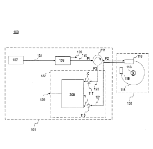
[0021] FIG. 1 is an illustration of a fiber-optic current system 100
transducer according
to an exemplary embodiment. The FOCT includes a sensor module 105 and a
receiver/decoder module 101. The sensor module 105 includes a fiber 115
positioned
around conductor 113. The receiver module 101 includes a light source 107 that
produces
a non-polarized light beam 131 for input to an optical splitter 109. The
optical splitter 109
is configured to split the light beam 131 into multiple outputs, of which only
two are shown
(125 and 126).
CA 02925248 2016-03-29
276985
[0022] Output 126 is fed to an optical circulator 111 that allows light to
enter a first
port (P1) and to exit through a second port (P2). Light returning to the
second port (P2) of
optical circulator 111 is directed to a third port (P3) of optical splitter
109 of the fiber optic
sensor 105 via optical module 118. Light beam 131 is coupled to fiber 115 and
serves as a
probe light beam that changes polarization when current flows in conductor
113. The light
in fiber 115 is reflected back into the fiber using an end mirror 116 and back
to the receiver
101 via path 123 and path 121. Paths 123 and 121 can be implemented using
optical fibers
or numerous other wave guiding devices known in the art.
[0023] As stated above, the light in fiber 115 is reflected back to
receiver 101. A
processing unit 132 included in receiver 101 is configured to process the
reflected light to
provide (at terminal 129) a measure of the current in conductor 113.
Processing unit 132
includes transducers 117 and 119. These transducers are configured to convert
the light
beams from path 123 and path 121 into electrical signals X and Y,
respectively.
[0024] Transducers 117 and 119 can be implemented using PIN diodes. By way
of
example, and not by limitation, each PIN diode may have a responsivity in the
range of
about 0.1 [Ampere/Watt] ([A/W]) to about 1 [A/W]. The transducers can also be
implemented using other types of photodetector configurations. For example, p-
n
junctions, photogates, active or passive pixel sensors can be used to
implement each of
transducer 117 and 119. In general, any phototransducer can be used without
departing
from the scope contemplated in the present disclosure.
[0025] Processing unit 132 includes a system 200 configured to process
electrical
signals X and Y to produce an output signal at terminal 129, the output signal
being
indicative of the current in conductor 113. While only terminal 129 is shown
in FIG. 1 as
an output of processing unit 132 (and of system 200), other output terminals
may be
present. This may be a digital value stored in memory or an analog value from
a D/A
converter. Furthermore, while transducers 117 and 119 are shown to be separate
from
system 200, in some implementations, these transducers can be part of system
200.
6
CA 02925248 2016-03-29
276985
[0026] FIG. 2A is an illustration of system 200, as discussed above with
respect to FIG.
1. It is noted that system 200 can be implemented using discrete integrated
circuits such as
analog-to-digital (A/D) converters, digital-to-analog (DAC) converters,
multiplexers
(MUX), amplifiers, integral regulators, push-pull regulators, summing
junctions, and the
like. System 200 can also be implemented using one or more programmable
embedded
systems (see FIG. 3). The one or more embedded systems can provide the
functionalities
that will be discussed below with respect to system 200, FIG. 2A, and FIG. 2B.
[0027] System 200 functions as a decoder, in that it decodes information
contained in
electrical signals X and Y. These signals are representative of the light
beams reflected to
receiver 101 from fiber 115. System 200 can include a processor (not shown)
and a memory
(not shown). The processor can be programmed to execute instructions from the
memory
to control the various components of system 200 shown in FIG. 2A and FIG. 2B.
For
example, the processor can be programmed to select the gain of the various
gain stages of
system 200. Signal values can also be stored in the memory to allow further
processing
and/or data logging. The memory can be co-located with the processor and the
other
components of system 200.
[0028] At power up, system 200 undergoes an initialization and calibration
process
wherein inherent offsets of DAC modules and AID modules are cancelled. During
initialization and calibration, the gain of gain stage 201 is set to 1 (or to
zero, considering
the small current input signal), since the gain during operation is normally
greater than 10,
000. The inherent offset in DAC 221 is determined by taking data at two
different gains
using gain stage 203. This inherent offset is then removed by offsetting the
output of DAC
221 and it is added to any signal inputted to DAC 221. After calibrating DAC
221, the
offset of AID 217 are calculated and stored in the memory. A similar procedure
is
undertaken using gain stages 209 and 211, DAC 225 and A/D 219.
[0029] System 200 includes two signal paths, each reserved for one of
electrical signal
X and electrical signal Y. Each of these signal paths forms a channel. The
path for electrical
signal X (hereafter the "X-signal path," or the "X-channel") includes a first
gain stage 201
7
= CA 02925248 2016-03-29
276985
that buffers signals X. Gain stage 201 can be programmed to amplify electrical
signal X.
When signal X is a current (i.e. a photocurrent in transducer 117), gain stage
201 converts
electrical signals X into a voltage signal.
[0030] Gain stage 201 is a variable gain stage. During operation of system
200, the
processor steps through several gain values supported by gain stage 201 until
the output of
gain stage 201 reaches an optimum value. For example, the optimum value may
correspond
to the output of gain stage 201 reaching a voltage that is in the range of
about 4 Volts to
about 6 Volts. The optimum value can also be a predetermined target voltage
and the
processor may stop stepping through the gain values of gain stage 201 when the
output
voltage is within a tolerance of the predetermined target voltage.
[0031] The integral regulator 233 forces the output of summing junction 202
to be zero.
Thus, the output of integral regulator 233 represents the DC offset contained
in electrical
signal X. By forcing the output of summing junction 202 to zero, the gain of
gain stage 203
(which is also a variable gain stage) can be large without saturating AID 217.
[0032] Similarly, in the path for electrical signal Y (i.e. the "Y-signal
path," or the "Y-
channel"), there is a gain stage 209 that is a variable gain stage. The
processor steps through
several gain values supported by gain stage 209 until the output of gain stage
209 reaches
an optimum value. As before, the optimum value may correspond to the output of
gain
stage 209 reaching a voltage that is in the range of about 4 Volts to about 6
Volts. The
optimum value can also be a predetermined target voltage and the processor may
stop
stepping through the gain values of gain stage 209 when the output voltage is
within a
tolerance of the predetermined target voltage.
[0033] The integral regulator 231 forces the output of summing junction 204
to be zero.
Thus, the output of integral regulator 231 represents the DC offset contained
in electrical
signal Y. By forcing the output of summing junction 204 to zero, the gain of
gain stage 211
(which is also a variable gain stage) can be large without saturating AID 219.
8
CA 02925248 2016-03-29
276985
[0034] System 200 also includes a MUX 207 in the X-signal path. MUX 207
multiplexes several X-channels into driver 205, which drives AID 217. Inputs
of MUX 207
can also include power supply data which can serve to force the output of
driver 205 to a
power supply rail. In some implementations, MUX 207 can be a 16-to-1
multiplexer.
[0035] The output 235 of AID 217 is fed to the input path of integral
regulator 233.
AID 217 can be an 18-bit converter. It is noted that AID configurations such
as flash or
sigma-delta or any other AID architecture can be used without departing from
the scope of
the present disclosure. Further, Y-signal path includes components similar in
architecture
and function to the above-mentioned components of the X-signal path. For
example, the
Y-signal path includes a MUX 213, which can also be used to interface system
200 with
multiple Y-signal paths originating from a plurality of FOCTs. Driver 215
drives AID 219,
much like driver 205 drivers AID 217. The Output 237 of AID 219 is fed to the
input path
of integral regulator 231 for further processing. Furthermore, it is noted
that AID 217 and
AID 219 must be synchronized so that the X and Y signals are sampled at the
same instance
in time. If not then an error occurs, which prevents the two signal from being
added or
subtracted correctly.
[0036] System 200 also includes several components in the input path of the
integral
regulators 233 and 231. For example, the output signal 235 is scaled by a
factor of "-I" and
by a factor of "1/G2" before being fed to a summing junction at the input of
integral
regulator 233. The scaling factor of "4" is used because A/D drivers 205 and
215 are
inverting operational amplifiers. In another embodiment, non-inverting
amplifiers can be
used to implement drivers 205 and 215, in which the proper scaling factor
would be "+1."
[0037] The two scaling factors effectively scale the signal of output 235
to provide
signal 239, which represents the raw X-signal but in a digital format.
Similarly, in the input
path of integral regulator 231, output signal 237 is scaled by a factor of"-l"
and by a factor
of "1/G2" to provide signal 241, which represents the raw Y-signal, which is
also in digital
format. It is noted that G2 is the gain of stage 203 or that of stage 211.
During operation,
both stages have identical gains. However, generally speaking, gain stages 203
and 211 do
9
CA 02925248 2016-03-29
276985
not need to have the same gain, as these gains can be cancelled by adjusting
the signal in
each path with the reciprocal value of its corresponding gain. Such
adjustments mean that
outputs 239 and 241 are in engineering units. It is noted that other unit
systems can be used
without departing from the scope of the present disclosure.
[0038] The "n/k" ratio in blocks 247 and 249 in each of the input paths of
integral
regulators 233 and 231 represent the voltage resolution at which the signal
can be observed
on each of the input paths. This voltage resolution is governed by the number
of
quantization levels of AID 217 and AID 219. For instance, in blocks 247 and
249, "n" can
be 10, indicating a maximum voltage swing of 10 Volts, and "k" can be 131,071,
representing the number of quantization levels of 18-bit AID 217 and AID 219.
It is noted
that 10 V corresponds to 131,071 and -10V corresponds -131,071, thereby
allowing bipolar
operation. Furthermore, it is noted that these values of "n" and "k" are
exemplary; they can
be changed without departing from the scope of the present disclosure.
[0039] System 200 also includes DAC 221 and 225, which convert the outputs
of
integral regulators 233 and 231 to analog signals before input to summing
junctions 204
and 202. The ratios "m/n" in blocks 227 and 223 merely indicate resolution of
the digital-
to-analog conversion. For example, "m" can be 32,767, presenting the number of
analog
levels of either of DAC 221 and DAC 225, and "n" can be 10, indicating a
maximum
voltage of 10 Volts.
[0040] During operation of system 200, the nominal power returned on the Y-
signal
path is different than the nominal power returned on the X-signal path since
different losses
can occur in each of the channels. These losses correspond to a gain of less
than 1. As such,
push-pull regulator 229 is configured to adjust the gain in both the X-signal
path and the
Y-signal path to force each of electrical signal X and electrical signal Y to
be on the same
per-unit basis. This occurs via the summing junctions 242 and 244 and by
scaling the
outputs of integral regulators 233 and 231. This compensates for losses due to
temperature
variations, crystal offsets and other losses found in the optical components.
CA 02925248 2016-03-29
276985
[0041] Once push-pull regulator 229 has corrected the gain, electrical
signal Y can then
be subtracted from the electrical signal X, and any DC component will be
eliminated.
Signals 243 and 245 correspond respectively to the DC offset in electrical
signal X and
electrical signal Y, respectively. Push-pull regulator 229 ensures that offset
removal can
still be performed when there is a sudden change in the output power of light
source 107.
This is important since, in some implementations, integral regulators 233 and
231 may be
relatively slow in forcing the outputs of summing junctions 202 and 204 to
zero. Thus, as
a result of the operation of push-pull regulator 229, any AC component that
would appear
in the measured current due to distortions will be removed.
[0042] System 200 can be configured to provide accurate current
measurements in a
low current regime and in a high current regime. For instance, when the X and
Y signals
are added to obtain the measured current, their AC component is cancelled and
only the
DC component remains. This occurs when the current in conductor 113 is in the
low current
regime, i.e. below approximately 4,000 A (rms).
[0043] In the high current regime (i.e. for a current in conductor 113 that
is greater than
4,000 A (rms)), the area of the negative section of the AC waveform in the
measured
current is greater than the area of in its positive section. The difference
between these two
areas grows with larger currents. As such, during large current measurements,
the DC
signal will be dominated by the negative portion of the current, and will have
a fundamental
frequency twice that of the waveform in the negative section.
[0044] Thus, if the DC signal is low pass filtered, the output will decay
with large
current measurements. This decay corresponds to a perceived decrease in steady
state light
power. System 200 can be configured to detect a maximum value in each cycle
required to
capture the true power value of the light source. This occurs using the ratio
of the maximum
value to the perceived power value as a current correction factor. This
eliminates the non-
linear error to 1 pu current, i.e. to the level of current that causes a 45
degree change in the
steady state value. A sub-system 260 of system 200 that can achieve these
function is
described below, with respect to FIG. 2A.
11
CA 02925248 2016-03-29
276985
[0045] Sub-system 260 (FIG. 2B) makes use of the extracted DC offset from
the X
signal (signal 243), the extracted DC offset from the Y signal (signal 245),
the output of
the push-pull regulator 229 (i.e. signal 251), the raw X signal 239, and the
raw Y signal
241. The raw signals are multiplied by output 251 to place the signals on the
same per unit
base, then they are combined with their corresponding DC offset. The resulting
composite
signal is then fed to block 261 which is configured to detect a maximum in the
current
cycle of the composite signal. When the signals are on the same per unit base
they can be
added or subtracted. When the signals are added, the AC portion of the signal
is cancelled.
When the signals are subtracted, the DC component is eliminated. One of skill
in the
relevant art(s) will readily recognize common means for dynamically detecting
maximum
values (on a per cycle basis) from a signal can be used to implement block
261. For
example, a peak detector can be used to implement block 261.
[0046] Once the maximum value in the current cycle is detected, the
composite signal
is corrected with a correction factor 271 computed by sub-system 260. The
computation is
achieved using a plurality of summing junctions, multiplying junctions, and
division
junctions (267, 265, 269), and with a maximum value selector 263 (with a
minimum value
of 1 and the input). The DC power is scaled by a factor of 2 going into
division junction
265. The corrected output current 129 (also shown in FIG. 1) is a high-
fidelity measurement
of the current induced in conductor 113.
[0047] FIG. 3 is an illustration of system 300 according to an embodiment.
System 300
can perform all the functions described above with respect to system 200.
Furthermore,
system 300 is an application-specific system implemented using programmable
hardware.
The functions of system 300 can be programmed in software and/or firmware that
can be
loaded onto a computer-readable medium which can be read by system 300 to
cause system
300 to execute one or more of the functions.
[0048] System 300 can be implemented using at least one of a system-on-a-
chip (SoC),
an embedded computer, and a microcontroller. System 300 can include a
processing unit
coupled to a memory device. The memory can have instructions stored thereon,
the
12
CA 02925248 2016-03-29
276985
instructions being configured to cause the processing unit to execute the
various functions
described above with respect to system 200.
[0049] System 300 can include one or more hardware and/or software (or
firmware)
components configured to fetch, decode, execute, store, analyze, distribute,
evaluate,
and/or categorize information relating to the various functions and
applications discussed
herein. In some embodiments, the entirety of system 300 may be located
proximate to the
transmission line (i.e. conductor 113 in FIG. 1). In other embodiments, some
components
of system 300 may be located distant from the transmission line, i.e. away
from the
measurement site.
[0050] System 300 can include one or more processing unit 311, a storage
device 315,
a memory 301, an input/output (I/O) module 309, and a communication network
interface
313. System 300 can be connected to a communication network 317 via network
interface
313. As such, system 300 can be communicatively coupled to a database 319.
While FIG.
3 illustrates only one database (database 319), one of ordinary skill in the
relevant art(s)
will readily recognize that system 300 may be communicatively coupled to
several
databases.
[0051] System 300 can be configured to function as a client device that is
communicatively coupled to a server (not shown) via network 40. The server may
be
located at one data center, or distributed over a plurality of data centers.
In some
embodiments, I/O module 309 includes a keypad for user input. In other
embodiments, I/O
module 309 can include a touchscreen interface for input and one or more
displays for
visual output, such as a view screen.
[0052] Processing unit 311 can include one or more processing devices or
cores (not
shown). Further, as shown in FIG. 3, processing unit 311 can be
communicatively coupled
to storage device 315, memory 301, I/0 module 309, and network interface 313.
As such,
processing unit 311 may be configured to execute software or firmware
instructions,
routines, or sub-routines that are designed to cause processing unit 311 to
perform a variety
of functions and/or operations consistent with the embodiments of the present
disclosure.
13
CA 02925248 2016-03-29
276985
In one exemplary embodiment, instructions can be loaded into the various
modules of
memory 301 for execution by processing unit 311. Instructions can also be
fetched by
processing unit 311 from database 319, storage device 315, or they may be
provided to
processing unit 311 from I/O module 309.
[0053] Storage device 315 can include a volatile or non-volatile, magnetic,
semiconductor, tape, optical, removable, non-removable, read-only, random-
access, or
other type of storage device or computer-readable computer medium.
Furthermore, storage
315 can be configured to log data processed, recorded, or collected during the
operation of
system 300. The data can be time-stamped, cataloged, indexed, or organized in
a variety of
ways consistent with data storage practice without departing from the scope of
the present
disclosure.
[0054] Communication network interface 313 includes one or more components
configured to transmit and receive data via communication network 317. These
components can include one or more modulators, demodulators, multiplexers, de-
multiplexers, network communication devices, wireless devices, antennas,
modems, and
any other type of device configured to enable data communication via any
suitable
communication network. Furthermore, communication network 317 can be any
appropriate
network allowing communication between or among one or more computing systems,
such
as the Internet, a local area network, or a wide area network.
[0055] Memory 301 can include an initialization and calibration module 303
configured to cause processing unit 311 to initialize and calibrate system
300, as described
above with respect to system 200. Further, memory 301 can include an X-offset
removal
module 305 configured to cause processing unit 311 to receive an electrical
signal X from
one transducer (not shown) and to remove an offset from the electrical signal
X.
Furthermore, memory 301 can include a Y-offset removal module 307 configured
to cause
processing unit 311 to receive an electrical signal Y from another transducer
(not shown)
and to remove an offset from the electrical signal Y.
14
CA 02925248 2016-03-29
276985
[0056] Memory 301 can also include a normalizing module 308 configured to
normalize electrical signal Y and electrical signal X, wherein normalization
includes
making electrical signal X and electrical signal Y to be on the same per unit
basis. In sum,
while only a few modules are described in relation to memory 301, it should be
understood
that all of the functions of system 200 can be implemented in the form of
modules of
memory 301. Moreover, memory 301 can include a linearizing module 310 that is
configured to correct non-linearities in the output current as described with
respect to sub-
system 260.
[0057] Having set forth the structure and function of system 200 and the
various
modules included in exemplary system 200, operations consistent with
embodiments of the
present disclosure are now described. Such operations can include executing a
method of
removing a DC offset using the exemplary systems previously described.
[0058] FIG. 4 is a flow chart illustrating a method 400, according to an
embodiment.
Method 400 can be executed using the exemplary systems described above.
Further, it may
be used to remove offsets in electrical signals as well adjusting one or more
electrical
signals to be on the same per unit basis. It is noted that while method 400 is
discussed in
the context of electrical signals transduced from FOCT light signals, method
400 is not
limited to only such applications. Specifically, method 400 can be used for
any application
in which offset removal and signal normalizing is required.
[0059] Method 400 includes receiving, by a system like the ones disclosed
herein, a
first light signal. Further, method 400 includes transducing the first light
signal into a first
electrical signal, which can be the X-signal, as described above (401). Method
400 also
includes receiving a second light signal and transducing the second light
signal into a
second electrical signal, which can be the Y-signal, as described above (401).
[0060] Method 400 then includes adjusting the first electrical signal and
the second
electrical signal until both electrical signals are on the same per unit basis
(403).
Furthermore, method 400 can also include removing offsets present in each of
the adjusted
first electrical signal and second electrical signal (405).
CA 02925248 2016-03-29
276985
[0061] In some embodiments, method 400 can include monitoring a difference
in DC
offsets between the first electrical signal and the second electrical signal
(407). Moreover,
as a result of monitoring the DC offsets, method 400 can include altering the
first electrical
signal and the second electrical signal until both signals are equal.
Adjusting the electrical
signals may include altering the first electrical signal and the second
electrical signal by
providing a gain to multiply each of the signals until both are equal.
Furthermore, adjusting
the signals can include normalizing the first electrical signal and the second
electrical.
[0062] Method 400 can also combining the first electrical signal and the
second
electrical signal into a composite signal that is offset free (409).
Furthermore, memory 301
can include linearizing the composite signal (411) and subsequently producing
a high-
fidelity output of the current induced in a conductor proximate to the FOCT
based on the
linearized composite signal (413).
[0063] While there have been described herein what are considered to be
preferred and
exemplary embodiments of the present invention, other modifications of these
embodiments falling within the scope of the invention described herein shall
be apparent
to those skilled in the art.
16