Note: Descriptions are shown in the official language in which they were submitted.
METHODS FOR FORMING LIPID BILAYERS ON BIOCHIPS
CROSS-REFERENCE
[001] This application claims the benefit of U.S. Provisional Application No.
61/894,661,
entitled "Methods for Forming Lipid Bilayers on Biochips," filed 23 October
2013.
BACKGROUND
[002] Biochips can be used for various kinds of molecular detection and
sensing,
including the sequencing of nucleic acid molecules. Nucleic acid sequencing is
a
process that may be used to provide sequence information for a nucleic acid
sample.
Such sequence information may be helpful in diagnosing and/or treating a
subject. For
example, the nucleic acid sequence of a subject may be used to identify,
diagnose and
potentially develop treatments for genetic diseases. As another example,
research into
pathogens may lead to treatment for contagious diseases.
[003] There are methods available which may be used to sequence a nucleic
acid.
Such methods, however, are expensive and may not provide sequence information
within a time period and at an accuracy that may be necessary to diagnose
and/or treat
a subject.
SUMMARY
[004] Nanopores can be used to detect various molecules, including but not
limited to
sequencing polymers such as nucleic acid molecules. Recognized herein is the
need for
improved biochips and methods for making biochips {e.g., comprising
nanopores). In
some cases, conventional semiconductor processing techniques are deficient in
producing a silicon device for use as a biochip. For instance, methods are
provided that
can produce a biochip that withstands {e.g., is operable during or after
contact with)
highly corrosive environments such as aqueous solutions, e.g., comprising
ions. In
another aspect, the methods described herein create a biochip surface
conducive to the
formation of organic membranes (e.g., lipid bilayers). In another aspect, the
methods
provide electrochemical electrodes needed to perform electrical measurements
of ionic
current flows in the biochip.
[005] Amongst other things, the biochips produced according to the methods
described
herein can be used for nucleic acid molecule identification and polymer (e.g.,
nucleic
- 1 -
Date Recue/Date Received 2021-03-18
CA 02926124 2016-03-31
WO 2015/061510 PCT/US2014/061853
acid) sequencing. In some instances, the polymer is passed through the
nanopore and
various subunits of the polymer (e.g., adenine (A), cytosine (C), guanine (G),
thymine
(T) and/or uracil (U) bases of the nucleic acid) affect the current flowing
through the
nanopore. As described herein, the various subunits can be identified by
measuring the
current at a plurality of voltages applied across the nanopore and/or
membrane. In some
cases, the polymerization of tagged nucleotides releases and/or presents tag
molecules
to the nanopore that can be identified by measuring the current at a plurality
of voltages
applied across the nanopore and/or membrane.
[006] In an aspect, the disclosure provides a method for forming a lipid
bilayer for use
in a nanopore sensing device, comprising: (a) providing a chip comprising a
fluid flow
path in fluid communication with a plurality of sensing electrodes; (b)
flowing a lipid
solution into the fluid flow path; and (c) flowing at least one bubble onto
the fluid flow
path, thereby forming a lipid bilayer adjacent to the sensing electrodes,
wherein the
bubble spans the plurality of sensing electrodes, and wherein the bubble is
adjacent to
the sensing electrodes for at least about 1 second. In some embodiments, the
bubble is
adjacent to the sensing electrodes for between about 'inns to about 5 minutes.
[007] In some embodiments, the bubble is adjacent to the sensing electrodes
for at
least about 30 seconds. In some embodiments, the bubble is adjacent to the
sensing
electrodes for at most about 5 minutes. In some embodiments, a lipid bilayer
is formed
over at least 50% of the sensing electrodes. In some embodiments, a lipid
bilayer is
formed over at least 70% of the sensing electrodes.
[008] In some embodiments, the method further comprises inserting a nanopore
into
the lipid bilayers adjacent to each of the sensing electrodes. In some
embodiments, the
chip comprises wells, and wherein the sensing electrodes are in the wells.
[009] In another aspect, the disclosure provides a method for forming a lipid
bilayer for
use in a nanopore sensing device, comprising: (a) providing a chip comprising
a fluid
flow path in fluid communication with a plurality of sensing electrodes; (b)
flowing at
least one bubble into the fluid flow path and adjacent to said plurality of
sensing
electrodes such that the bubble spans the plurality of sensing electrodes; and
(c)
contacting the periphery of the bubble with a lipid, wherein the lipid
diffuses under the
bubble and onto the fluid flow path, thereby forming a lipid bilayer adjacent
to the
sensing electrodes.
[0010] In some embodiments, the bubble is contacted with the lipid for at
least about 30
seconds. In some embodiments, the bubble is contacted with the lipid for
between about
5ms to about 5 minutes. In some embodiments, a lipid bilayer is formed over at
least
-2-
CA 02926124 2016-03-31
WO 2015/061510 PCT/US2014/061853
70% of the sensing electrodes. In some embodiments, the method further
comprises
inserting a nanopore into the lipid bilayers adjacent to each of the sensing
electrodes. In
some embodiments, the nanopore is Mycobacterium smegmatis porin A (MspA),
alpha-
hemolysin, any protein having at least 70% homology to at least one of
Mycobacterium
smegmatis porin A (MspA) or alpha-hemolysin, or any combination thereof.
[0011] In some embodiments, inserting the nanopore comprises applying an
electrical
stimulus through said electrode to facilitate the insertion of said nanopore
in said lipid
bilayer. In some embodiments, said lipid bilayer exhibits a resistance greater
than about
1 GS2.
[0012] In some embodiments, said lipid bilayer and said nanopore protein
together
exhibit a resistance of about 1 Go, or less. In some embodiments, said lipid
comprises
an organic solvent. In some embodiments, said bubble is a vapor bubble. In
some
embodiments, the chip comprises wells, and wherein the sensing electrodes are
in the
wells.
[0013] In some embodiments, said lipid is selected from the group consisting
of
diphytanoyl-phosphatidylcholine (DPhPC), 1,2-diphytanoyl-sn-glycero-
3phosphocholine,
1,2-Di-O-Phytanyl-sn-Glycero-3-phosphocholine (DoPhPC), palmitoyl-oleoyl-
phosphatidyl-choline (POPC), dioleoyl-phosphatidyl-methylester (DOPME),
dipalmitoylphosphatidylcholine (DPPC), phosphatidylcholine,
phosphatidylethanolamine,
phosphatidylserine, phosphatidic acid, phosphatidylinositol,
phosphatidylglycerol,
sphingomyelin, 1,2-di-O-phytanyl-sn-glycerol; 1,2-dipalmitoyl-sn-glycero-3-
phosphoethanolamine-N-[methoxy(polyethylene glycol)-350] ; 1,2-dipalmitoyl-sn-
glycero-3-phosphoethanolamine-N-[methoxy(polyethylene glycol)-550]; 1,2-
dipalmitoyl-
sn-glycero-3-phosphoethanolamine-N-[methoxy(polyethylene glycol)-750]; 1,2-
dipalmitoyl-sn-glycero-3-phosphoethanolamine-N-[methoxy(polyethylene glycol)-
1000];
1,2-dipalmitoyl-sn-glycero-3-phosphoethanolamine-N-[methoxy(polyethylene
glycol)-
2000]; 1,2-dioleoyl-sn-glycero-3-phosphoethanolamine-N-lactosyl; GM1
Ganglioside,
Lysophosphatidylcholine ([PC) or any combination thereof.
[0014] In another aspect, the disclosure provides a nanopore sensing system,
comprising: (a) a chip comprising a fluid flow path in fluid communication
with a plurality
of sensing electrodes, wherein each of said sensing electrodes is configured
to detect
an ionic current upon a nucleic acid incorporation event; and (b) a control
system
coupled to said chip, said control system programmed to: (i) flow a lipid
solution into the
fluid flow path; (ii) flow at least one bubble into the fluid flow path and
adjacent to the
sensing electrodes for a time period of at least about 1 second, wherein the
bubble
-3-
spans the plurality of sensing electrodes, and wherein the flow of the bubble
into the
fluid flow path forms a lipid bilayer adjacent to the sensing electrodes. In
some
embodiments, the bubble is adjacent to the sensing electrodes for a time
period of
between about 5 ms to about 5 minutes.
[0015] In some embodiments, the chip comprises wells, and wherein the sensing
electrodes are in the wells. In some embodiments, the control system is
external to said
chip. In some embodiments, the control system comprises a computer processor.
In
some embodiments, the method further comprises a fluid flow system operably
coupled
to said control system and said chip, wherein said fluid flow system is
configured to
direct the flow of said lipid solution and said bubble.
[0016] Additional aspects and advantages of the present disclosure will become
readily
apparent to those skilled in this art from the following detailed description,
wherein only
illustrative embodiments of the present disclosure are shown and described. As
will be
realized, the present disclosure is capable of other and different
embodiments, and its
several details are capable of modifications in various obvious respects, all
without
departing from the disclosure. Accordingly, the drawings and description are
to be
regarded as illustrative in nature, and not as restrictive.
BRIEF DESCRIPTION OF THE DRAWINGS
[0018] The novel features of the invention are set forth with particularity in
the appended
claims. A better understanding of the features and advantages of the present
invention
will be obtained by reference to the following detailed description that sets
forth
illustrative embodiments, in which the principles of the invention are
utilized, and the
accompanying drawings of which:
[0019] Figure 1 shows a pore-based electrosensor;
[0020] Figure 2 shows a nanopore biochip;
[0021] Figure 3 shows an electrode array where the container doubles as a
counter
electrode;
[0022] Figure 4 shows an electrode array with a common counter electrode;
-4 -
Date Recue/Date Received 2021-03-18
CA 02926124 2016-03-31
WO 2015/061510 PCT/US2014/061853
[0023] Figure 5 shows an electrode array where strips of sensors share a
common
counter electrode;
[0024] Figure 6 shows and electrode array where each electrode has an
independent
counter electrode;
[0025] Figure 7 shows an example of rows of sensor wells sharing a common
electrolyte pool;
[0026] Figure 8 shows an example of a semiconductor substrate;
[0027] Figure 9 shows a layer of silicon dioxide deposited on a semiconductor
substrate;
[0028] Figure 10 shows a photo-resist deposited on a silicon dioxide layer;
[0029] Figure 11 shows an area of the photo-resist being exposed to radiation
to define
the area of a well;
[0030] Figure 12 shows a portion of the silicon dioxide being removed by a dry
etch
procedure;
[0031] Figure 13 shows additional silicon dioxide being removed by a wet etch
procedure to create a well;
[0032] Figure 14 shows deposition of a titanium adhesion layer;
[0033] Figure 15 shows deposition of a titanium Nitride protective layer with
Platinum
protective layer or alternately Platinum serving as the electrode;
[0034] Figure 16 shows deposition of silver electrode material;
[0035] Figure 17 shows lift off of the photo-resist and materials disposed
thereupon;
[0036] Figure 18 shows silanization of the silicon dioxide;
[0037] Figure 19 shows the filling of the well with a gel;
[0038] Figure 20 shows creation of a membrane with a nanopore over the well;
[0039] Figure 21 shows a biochip where the silver electrode comes up on the
side walls
of the well;
[0040] Figure 22 shows a large bubble held adjacent to a plurality of
electrodes;
[0041] Figure 23 shows an example of a method for forming a lipid layer over
the
electrodes on one or more flow channels of the primed sensor chip;
[0042] Figure 24 shows an example of a semiconductor sensor chip;
[0043] Figure 25 shows an example flowcell configuration;
[0044] Figure 26 shows an example of a packaged chip; and
[0045] Figure 27 shows an example of bilayer formation and pop automated with
a
pump.
-5-
CA 02926124 2016-03-31
WO 2015/061510 PCT/US2014/061853
[0046] Figure 28 is a flowchart for an automatic chip setup. This test would
confirm that
the majority of cells on the chip are acceptable. If an insufficient number of
cells (as
determined by the operator) pass the test, then the entire chip will fail.
[0047] Figure 29 is a flowchart for an automatic pump for bilayer formation.
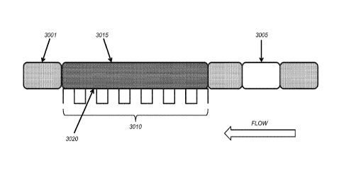
[0048] Figure 30 is an illustration of the flow of various solutions and/or
bubbles over the
wells of a sensor chip. The direction of flow is indicated by the block arrow
in the lower
right corner of the diagram. In this figure, the first rectangle representing
ionic solution
(3001; divot patterned rectangle) has already flowed over the wells (3010),
the lipid
solution (3015; cross-hatched rectangle) is on the chip (and in this depiction
covers all of
the wells), and the second and third rectangles representing ionic solution,
as well as
the bubble (3005; clear rectangle) have not yet been flowed onto the chip. The
size of
the rectangles is not representative of the amount of the fluid or size of the
bubble. The
ionic solution-bubble- ionic solution sequence may be repeated several times
in order to
increase the bilayer coverage, decrease the non-bilayer coverage, e.g., multi-
layer
stacks of lipids on the wells, and/or reestablish the bilayer after a pop
test. The lipid
bilayer will form at the interface (3020) of the wells (shown) or
substantially planar
electrodes (not shown) once the method described herein is performed.
DETAILED DESCRIPTION
[0049] While various embodiments of the invention have been shown and
described
herein, it will be obvious to those skilled in the art that such embodiments
are provided
by way of example only. Numerous variations, changes, and substitutions may
occur to
those skilled in the art without departing from the invention. It should be
understood that
various alternatives to the embodiments of the invention described herein may
be
employed.
[0050] The term "nanopore," as used herein, generally refers to a pore,
channel or
passage formed or otherwise provided in a membrane. A membrane may be an
organic
membrane, such as a lipid bilayer, or a synthetic membrane, such as a membrane
formed of a polymeric material. The membrane may be a polymeric material. The
nanopore may be disposed adjacent or in proximity to a sensing circuit or an
electrode
coupled to a sensing circuit, such as, for example, a complementary metal-
oxide
semiconductor (CMOS) or field effect transistor (FET) circuit. In some
examples, a
nanopore has a characteristic width or diameter on the order of 0.1 nanometers
(nm) to
about 1000 nrri. Some nanopores are proteins. Alpha hemolysin is an example of
a
protein nanopore.
-6-
CA 02926124 2016-03-31
WO 2015/061510
PCT/US2014/061853
[0051] The term "polymerase," as used herein, generally refers to any enzyme
capable
of catalyzing a polymerization reaction. Examples of polynnerases include,
without
limitation, a nucleic acid polymerase or a ligase. A polymerase can be a
polymerization
enzyme.
[0052] The term "nucleic acid," as used herein, generally refers to a molecule
comprising
one or more nucleic acid subunits. A nucleic acid may include one or more
subunits
selected from adenosine (A), cytosine (C), guanine (G), thymine (T) and uracil
(U), or
variants thereof. A nucleotide can include A, C, G, T or U, or variants
thereof. A
nucleotide can include any subunit that can be incorporated into a growing
nucleic acid
strand. Such subunit can be an A, C, G, T, or U, or any other subunit that is
specific to
one or more complementary A, C, G, T or U, or complementary to a purine (i.e.,
A or G,
or variant thereof) or a pyrimidine C, T or
U, or variant thereof). A subunit can
enable individual nucleic acid bases or groups of bases (e.g., AA, TA, AT, GC,
CG, CT,
TC, GT, TG, AC, CA, or uracil-counterparts thereof) to be resolved. In some
examples,
a nucleic acid is deoxyribonucleic acid (DNA) or ribonucleic acid (RNA), or
derivatives
thereof. A nucleic acid may be single-stranded or double stranded.
[0053] A "polynucleotide" or "oligonucleotide" is a polymer or oligomer
comprising one or
more nucleotide as defined herein. A polynucleotide or oligonucleotide may
comprise a
DNA polynucleotide or oligonucleotide, a RNA polynucleotide or
oligonucleotide, or one
or more sections of DNA polynucleotide or oligonucleotide and/or RNA
polynucleotide or
oligonucleotide.
[0054] As used herein, a "nucleotide" or "base" can be a primary nucleotide or
a
nucleotide analog. A primary nucleotide is deoxyadenosine mono-phosphate
(dAMP),
deoxycytidine mono-phosphate (dCMP), deoxyguanosine mono-phosphate (dGMP),
deoxythymidine mono-phosphate (dTMP), adenosine mono-phosphate (AMP), cytidine
mono-phosphate (CMP), guanosine mono-phosphate (GMP) or uridine mono-phosphate
(UMP). A nucleotide analog is an analog or mimic of a primary nucleotide
having
modification on the primary nucleobase (A, C, G, T and U), the
deoxyribose/ribose
structure, the phosphate group of the primary nucleotide, or any combination
thereof.
For example, a nucleotide analog can have a modified base, either naturally
existing or
man-made. Examples of modified bases include, without limitation, methylated
nudeobases, modified purine bases (e.g., hypoxanthine, xanthine, 7-
methylguanine,
isodG), modified pyrimidine bases (e.g., 5,6-dihydrouracil and 5-
methylcytosine, isodC),
universal bases (e.g., 3-nitropyrrole and 5-nitroindole), non-binding base
mimics (e.g., 4-
methylbezimidazole and 2,4-diflurotoluene or benzene), and no base (abasic
nucleotide
-7-
CA 02926124 2016-03-31
WO 2015/061510 PCT/US2014/061853
where the nucleotide analog does not have a base). Examples of nucleotide
analogs
having modified deoxyribose (e.g., dideoxynucleosides such as
dideoxyguanosine,
dideoxyadenosine, dideoxythymidine, and dideoxycytidine) and/or phosphate
structure
(together referred to as the backbone structure) includes, without limitation,
glycol
nucleotides, morpholinos, and locked nucleotides.
[0055] The term "(Y0 homology" is used interchangeably herein with the term
"(Y0 identity"
herein and refers to the level of nucleic acid or amino acid sequence identity
between
the nucleic acid sequence that encodes any one of the inventive polypeptides
or the
inventive polypeptide's amino acid sequence, when aligned using a sequence
alignment
program.
[0056] For example, as used herein, 80% homology means the same thing as 80%
sequence identity determined by a defined algorithm, and accordingly a
homologue of a
given sequence has greater than 80% sequence identity over a length of the
given
sequence. Exemplary levels of sequence identity include, but are not limited
to, 80, 85,
90, 95, 98% or more sequence identity to a given sequence, e.g., the coding
sequence
for any one of the inventive polypeptides, as described herein.
[0057] Exemplary computer programs which can be used to determine identity
between
two sequences include, but are not limited to, the suite of BLAST programs,
e.g.,
BLASTN, BLASTX, and TBLASTX, BLASTP and TBLASTN, publicly available on the
Internet. See also, Altschul, et al., 1990 and Altschul, et al., 1997.
[0058] Sequence searches are typically carried out using the BLASTN program
when
evaluating a given nucleic acid sequence relative to nucleic acid sequences in
the
GenBank DNA Sequences and other public databases. The BLASTX program is
preferred for searching nucleic acid sequences that have been translated in
all reading
frames against amino acid sequences in the GenBank Protein Sequences and other
public databases. Both BLASTN and BLASTX are run using default parameters of
an
open gap penalty of 11.0, and an extended gap penalty of 1.0, and utilize the
BLOSUM-
62 matrix. (See, e.g., Altschul, S. F., et al., Nucleic Acids Res. 25:3389-
3402, 1997.)
[0059] A preferred alignment of selected sequences in order to determine " /0
identity"
between two or more sequences, is performed using for example, the CLUSTAL-W
program in MacVector version 13Ø7, operated with default parameters,
including an
open gap penalty of 10.0, an extended gap penalty of 0.1, and a BLOSUM 30
similarity
matrix.
-8-
Biochips and nucleic acid sequencing
[0060] Pore based sensors (e.g., biochips) can be used for electro-
interrogation of single
molecules. A pore based sensor of the present disclosure can include a
nanopore
formed in a membrane that is disposed adjacent or in proximity to a sensing
electrode.
The sensor can include a counter electrode. The membrane includes a trans side
(i.e.,
side facing the sensing electrode) and a cis side (i.e., side facing the
counter electrode).
[0061] Reference will now be made to the figures, wherein like numerals refer
to like
parts throughout. It will be appreciated that the figures and features therein
are not
necessarily drawn to scale.
[0062] With reference to Figure 1 , a typical electrical measurement can
operate on a
molecule under test that is closely associated with a pore (e.g., binding can
be chemical,
mechanical, electrical, or electrochemical). The system can apply a stimulus
(voltage or
current) across the molecule/pore complex and measure the response. In order
to
isolate the measurement to the pore/molecule complex the two sides of the pore
are
generally separated by a highly insulating material (e.g., a lipid bilayer).
[0063] The volumes enclosed on the opposite sides of the insulating barrier
are referred
to as the cis well and the trans well with the general definition that the
species of interest
(e.g. , the nucleic acid molecule or tag molecule) moves from cis to trans
during
detection. The trans well is generally the side of the insulating membrane
proximal to
and electrically connected to the chip electrodes.
[0064] Figure 2 shows an example of a nanopore biochip (or sensor) having
temperature control, as may be prepared according to methods described in U.S.
Patent
Application Publication No. 201 1/0193570. With reference to Figure 2, the
nanopore
detector comprises a top electrode 201 in contact with a conductive solution
(e.g., salt
solution) 207. A bottom conductive electrode 202 is near, adjacent, or in
proximity to a
nanopore 206, which is inserted in a membrane 205. The membrane 205 can be
disposed over a well 210, or directly over an electrode, where the sensor 202
forms part
of the surface of the well. In some instances, the bottom conductive electrode
202 is
embedded in a semiconductor 203 in which is embedded electrical circuitry in a
semiconductor substrate 204. A surface of the semiconductor 203 may be treated
to be
hydrophobic. A molecule being detected goes through the pore in the nanopore
206. The
semiconductor chip sensor is placed in package 208 and this, in turn, is in
the vicinity of
a temperature control element 209. The temperature control element 209 may be
a
thermoelectric heating and/or cooling device (e.g., Peltier device). Multiple
nanopore
detectors may form a nanopore array.
- 9 -
Date Recue/Date Received 2021-03-18
CA 02926124 2016-03-31
WO 2015/061510 PCT/US2014/061853
[0065] In some embodiments, the biochip comprises a counter electrode capable
of
forming an electrical circuit with the electrode in the well. In some cases,
the plurality of
electrodes in the plurality of wells share a common counter electrode. Figure
3 shows
an electrode array having a common counter electrode where the liquid
containment
perimeter (e.g., container) acts as a counter electrode (e.g., is conductive
and forms a
circuit). Another embodiment of a counter electrode is shown in Figure 4,
where the
counter electrode is a plate (e.g., made of a conducting metal) over top of
the
nanopores. As shown in Figure 5 and Figure 6, the plurality of electrodes in
the plurality
of wells can be organized into groups that share a common counter electrode.
In some
cases, (e.g., Figure 6), the plurality of electrodes in the plurality of wells
each have a
dedicated counter electrode. In some cases, having a plurality of counter
electrodes can
allow an individual sensing electrode, or only a few sensing electrodes, to be
paired with
a single counter electrode and thus potentially improve the electrical
response and
performance of the sense-counter electrode pairs
[0066] In some cases, a plurality of wells (including any subset of the total
number of
wells) comprise a common electrolyte pool. As shown in Figure 7, the wells 701
may be
separated into rows by walls 702 such that the row of wells share a common
electrolyte
pool above the wells. Separating the biochip into sections as described here
can allow
multiple samples to be analyzed on a single biochip (e.g., by putting
different samples in
different sections of the chip).
[0067] A nanopore sensor can include at least 1, 2, 3, 4, 5, 6, 7, 8, 9, 10,
20, 30, 40, 50,
100, or 1000 nanopores (e.g., hennolysin or aquaporin, etc. or combinations
thereof)
adjacent to a electrode (e.g., the bottom conductive electrode 202). A
nanopore sensor
can include a top electrode (e.g., the top electrode 201) that is for sole use
by the
nanopore sensor (and not other sensors), or as an alternative, a top electrode
can be
provided for use by multiple nanopore sensors.
Biochip processing
[0068] Controlling surface characteristics, well cavity volume, and electrode
composition
and volume can be major challenges of developing a scalable semiconductor
based
planar array of microwells for the purpose of nanopore sensing. In some
instances, the
ideal nanopore based semiconductor array sensing platform would achieve the
following
goals: (1) chip surface characteristics that support a planar insulating
membrane, (2)
differentiated surface characteristics that result in a well-defined and well
controlled
planar membrane surface, (3) large trans-well electrolyte volume, (4) large
electrode
-10-
CA 02926124 2016-03-31
WO 2015/061510 PCT/US2014/061853
volume, (5)10w electrical cross-talk between adjacent sensor electrodes on the
array,
(6) high cell density in order to achieve very large array sizes, and (7)
stable
measurements of very long duration during which the key parameters (voltage,
resistance, etc.) remain nearly constant.
[0069] For example meeting goals (1) & (2) can be difficult as in particular
it can be
necessary to ensure that a highly insulating (resistive) barrier is formed
with well
controlled membrane areas and trans-well volumes.
[0070] In the case of forming a lipid bilayer membrane, the design and
processing of the
chip can be tailored to create hydrophobic (or lipophilic) surfaces and
hydrophilic (or
lipophobic) surfaces. Careful control of the chip surface allows well defined
hydrophilic
and hydrophobic areas to be defined. In turn this can control the structure
and
characteristics of the lipid bilayer membranes formed.
[0071] Goal (3) can be important in order to ensure that trans-well
electrolytic ions are
sufficiently abundant so as not to affect the results during the duration of a
typical
measurement. This could occur either by depleting one or the other of the ions
entirely
or shifting the relative concentration of the various ions to such a degree
that they
change the measurement results substantially (i.e., through shifts in
concentration
gradient and resulting Nernst potential).
[0072] Goal (4) can be important in the case of a sacrificial electrode that
is consumed
or converted as part of the electro-chemical reaction that supports the
measurement
(e.g. silver being converted to silver-chloride oxidation reaction). Having a
high electrode
volume can be important both to: (i) increase the time that a measurement can
be
continuously performed without intervening "recharging" measurements which may
disrupt the experiment completely or result in gaps in the measured data and
(ii) reduce
electrochemical potential shifts caused by the change in relative
concentrations of the
oxidized and reduced electrode components. In some cases, complete depletion
of the
electrode material (silver) sets a theoretical upper boundary on practical
continuous
measurement duration.
[0073] Unfortunately several of these goals can result in conflicts where
meeting one
goal comes at the expense of another. For example, etching a deep cavity in
the silicon
surface and filling completely with silver can achieve a planar membrane at
the
metal/silicon surface, thereby achieving goals (1), (2), and (4) however
leaves no
remaining volume available for trans-well electrolyte. Similarly, minimizing
electrical
cross-talk (goal 5) can be achieved by spacing adjacent cells far apart;
however this
comes at the expense of achieving goal (6).
-11-
CA 02926124 2016-03-31
WO 2015/061510 PCT/US2014/061853
[0074] In various aspects, the biochips and methods for making biochips
described
herein can achieve goals (1) to (6) in a way that is capable of sequencing
nucleic acid
molecules. For example, development of a deep well vertical cavity structure
to support
both electrolyte and electrode material can meet goals (3) and (4); a hybrid
wet/dry etch
can increase the lateral dimensions and thus trans well volume in can meet
goals (1),
(2), (3), and (4); selective silanization of oxide surfaces can achieve goals
(1) and (2);
utilization of a gel can be used to balance goals (3) and (4) while
simultaneously
achieving goals (1) and (2); implementation of distributed counter electrode
can
simultaneously achieve goals (5) and (6); use of electrode replenishment
(recharging)
can achieve goal (7); use of non-sacrificial electrodes (when feasible) can
achieve goal
(7); electro-plating can increase electrode material to meet goal (4); or any
combination
thereof.
Biochip characteristics
[0075] In an aspect, a biochip comprises (a) a semiconductor substrate; (b) a
layer of
silicon dioxide disposed on the substrate, wherein a well is formed into the
silicon
dioxide; (c) a corrosion resistant material coating the inside of the well;
(d) an electrode
material in the well filling some fraction of that well including completely
filling the oxide
well to be coplanar with the surface of the oxide; and (e) an organofunctional
alkoxysilane layer coating the silicon dioxide. In some embodiments, the
biochip further
comprises a membrane isolating a first fluid in the well from a second fluid
outside the
well. Also encompassed within the present invention are the biochips made by
any of
the methods described herein and the use of any of the biochips described
herein or
biochips produced by the methods described herein to sequence polymers,
including
but not limited to nucleic acid molecules.
[0076] In some cases, electrode material is not depleted during operation of
the biochip.
In an aspect, a biochip comprises a plurality of wells having a membrane
disposed over
the well and an electrode in the well that is capable of detecting changes in
the flow of
ions through a pore in the membrane in response to entities passing through
the pore,
wherein the electrode is not depleted during detection. In some embodiments,
the
electrode is substantially planar with the surface of the biochip, i.e., metal
fills the entire
well.
[0077] The electrode (e.g., silver or platinum material) can have any suitable
mass or
volume. In some cases, the volume of the electrode is about 0.1 femto-liter
(fL), about
0.5 fL, about 1 fL, about 5 fL, or about 10 fL. In some instances, the volume
of the
-12-
CA 02926124 2016-03-31
WO 2015/061510 PCT/US2014/061853
electrode is at least about 0.1 femto-liter (fL), at least about 0.5 fL, at
least about 1 fL, at
least about 5 fL, or at least about 10 fL. In some embodiments, the volume of
the
electrode is at most about 0.1 femto-liter (fL), at most about 0.5 fL, at most
about 1 fL, at
most about 5 fL, or at most about 10 fL.
[0078] The electrode can be made of any suitable material, including mixtures
and alloys
of materials. Some examples include platinum, silver, or any combination
thereof. In
some cases, the electrode material is not consumed during operation of the
electrode.
The electrode can comprise a material that has at least two oxidation states
and/or a
material that is capable of both accepting and donating electrons.
Chip with deep, closely packed wells
[0079] Having a high density of nanopore sensors on the biochip may be
desirable for
having a small device and/or sensing or sequencing a large number of molecules
with a
small biochip device. The surface comprises any suitable density of discrete
sites (e.g.,
a density suitable for sequencing a nucleic acid sample in a given amount of
time or for
a given cost). In an embodiment, the surface has a density of discrete sites
greater than
or equal to about 500 sites per 1 mm2. In some embodiments, the surface has a
density
of discrete sites of about 100, about 200, about 300, about 400, about 500,
about 600,
about 700, about 800, about 900, about 1000, about 2000, about 3000, about
4000,
about 5000, about 6000, about 7000, about 8000, about 9000, about 10000, about
20000, about 40000, about 60000, about 80000, about 100000, or about 500000
sites
per 1 mm2. In some embodiments, the surface has a density of discrete sites of
at least
about 200, at least about 300, at least about 400, at least about 500, at
least about 600,
at least about 700, at least about 800, at least about 900, at least about
1000, at least
about 2000, at least about 3000, at least about 4000, at least about 5000, at
least about
6000, at least about 7000, at least about 8000, at least about 9000, at least
about
10000, at least about 20000, at least about 40000, at least about 60000, at
least about
80000, at least about 100000, or at least about 500000 sites per 1 mm2.
[0080] A biochip with a high density of discrete sites generally results in a
well with a
small area. In some instances, the well is suitably deep (e.g., such that the
well has a
suitably large volume). In some instances, the well is substantially co-planar
with the
chip surface (i.e., metal fills the entire well). In an aspect, the volume of
the well is
suitably large such that ion concentration is not fully depleted in the well
before
recharging the electrode. In an aspect, the electrode can be a sacrificial
electrode (e.g.,
an electrode that decreases and/or increases in volume during detection, such
as silver)
-13-
CA 02926124 2016-03-31
WO 2015/061510 PCT/US2014/061853
and the volume of the well is suitably large such that the electrode is not
fully depleted
before recharging the electrode. In some embodiments, the well contains a
sufficiently
large volume of electrode material such as silver. In these aspects, amongst
others, the
volume of the well can limit the time for which the electrode is capable of
detecting a
current (i.e., before an ion is depleted and/or the electrode material is
depleted).
[0081] In some embodiments, the wells have a suitably large volume such that
the
electrode can detect ion flow (e.g., current) for about 50ps, about 100ps,
about 150ps,
about 200ps, about 250ps, about 300ps, about 350ps, about 400ps, about 450ps,
about
500ps, about 550ps, about 600ps, about 650ps, about 700ps, about 750ps, about
800ps, about 850ps, about 900ps, about 950ps, about 1 ms, about 5 ms, about 10
ms,
about 50 ms, about 100 ms, about 500 ms, about 1 s, about 5 s, about 10 s,
about 50 s,
about 100 s, about 500 s, about 1000s, or about 5000 s. In some embodiments,
the
wells have a suitably large volume such that the electrode can detect ion flow
(e.g.,
current) for at least about 50ps, at least about 100ps, at least about 150ps,
at least
about 200ps, at least about 250ps, at least about 300ps, at least about 350ps,
at least
about 400ps, at least about 450ps, at least about 500ps, at least about 550ps,
at least
about 600ps, at least about 650ps, at least about 700ps, at least about 750ps,
at least
about 800ps, at least about 850ps, at least about 900ps, at least about 950ps,
at least
about 1 ms, at least about 5 ms, at least about 10 ms, at least about 50 ms,
at least
about 100 ms, at least about 500 ms, at least about 1 s, at least about 5 s,
at least about
s, at least about 50 s, at least about 100 s, at least about 500 s, at least
about 1000
s, or at least about 5000 s.
[0082] By balancing the potential voltage applied across the electrode and
thereby
recharging or redistributing the ions on either side of the bilayer pore, the
data gathering
lifetime of the pore may be significantly extended to 10, 20, or 48 hours or
longer. An
example would be in nanopore system with 300mM KCI ionic solution at pH7.5, to
apply
+120mV across a bilayer pore for 30 seconds and then drop the voltage to -
120mV for
40 seconds. The cycle is repeated in this slow switching DC manner and the
ionic
charge distribution of the CIS and TRANS side of the bilayer pore remains
balanced, as
well as the the composition of Ag and AgCI present at one or more silver
electrodes also
maintains a balance. The result is a long life, data gathering pore detector.
The level or
magnitude of the positive and negatives voltages and the time spent in + or -
polarity
can be varied to suit the salt or ionic solution concentrations and the type
of pore that is
being used.
-14-
CA 02926124 2016-03-31
WO 2015/061510 PCT/US2014/061853
[0083] The time of detection can depend at least in part on the magnitude of
the voltage
applied across the nanopore and/or membrane (e.g., with higher voltage
magnitudes
resulting in higher ion current, faster depletion of electrodes and therefore
relatively
shorter detection periods). In some embodiments, the voltage difference across
the
membrane is from about OmV to about 1V, positive or negative, e.g., about 40
mV,
about 60 mV, about 80 mV, about 100 mV, about 120 mV, about 140 mV, about 160
mV, about 180 mV, about 200 mV, about 300 mV, about 400 mV, or about 500 mV.
In
some embodiments, the voltage difference across the membrane is at most about
40
mV, at most about 60 mV, at most about 80 mV, at most about 100 mV, at most
about
120 mV, at most about 140 mV, at most about 160 mV, at most about 180 mV, at
most
about 200 mV, at most about 300 mV, at most about 400 mV, or at most about 500
mV.
In some embodiments, the voltage difference across the membrane is at least
about
OmV to about 1V, positive or negative, e.g., at least about 40 mV, at least
about 60 mV,
at least about 80 mV, at least about 100 mV, at least about 120 mV, at least
about 140
mV, at least about 160 mV, at least about 180 mV, at least about 200 mV, at
least about
300 mV, at least about 400 mV, or at least about 500 mV. The voltage can be
constant
or variable (e.g., varying over any periodic waveform).
[0084] In some situations, the electrode has an operating life of at least
about 1 minute
("min"), 2 min, 3 min, 4 min, 5 min, 6 min, 7 min, 8 min, 9 min, 10 min, 15
min, 20 min,
30 min, 40 min, 50 min, 1 hour, 2 hours, 3 hours, 4 hours, 5 hours, 6 hours,
or 12 hours
under an applied potential of at least about OnnV to about 1V, positive or
negative, e.g.,
about 40 mV, about 60 mV, about 80 mV, about 100 mV, about 120 mV, about 140
mV,
about 160 mV, about 180 mV, about 200 mV, about 300 mV, about 400 mV, or about
500 mV. In some examples, the electrode has an operating life of at least
about 15 min
under an applied potential of about 80 mV.
[0085] The operating life of the electrode may be assessed based upon the
depletion
(e.g., rate of depletion) of the electrode during use. In some cases, the
electrode
material is depleted by at most about 50%, 40%, 30%, 20%, 10%, 9%, 8%, 7%, 6%,
5%, 4%, 3%, 2%, 1%, 0.1%, or 0.01% within a time period that is less than or
equal to
about 60 minutes, 30 minutes, 20 minutes, 15 minutes, 10 minutes, 5 minutes, 4
minutes, 3 minutes, 2 minutes, or 1 minute during use of the electrode. In
some
embodiments, the electrode material is not depleted within a time period that
is less than
or equal to about 60 minutes, 30 minutes, 20 minutes, 15 minutes, 10 minutes,
5
minutes, 4 minutes, 3 minutes, 2 minutes, or 1 minute during use of the
electrode.
-15-
CA 02926124 2016-03-31
WO 2015/061510 PCT/US2014/061853
[0086] The wells can have any suitable depth. In some cases, the depth of the
well is
measured from the surface of the biochip and/or bottom of the membrane to the
top of
the electrode and/or bottom of the electrode. In some cases, the depth of the
well is
approximately equal to the thickness of an oxide layer (e.g., 203 in Figure
2). In some
embodiments, the wells are about 0.5 micrometers (pm), about 1 pm, about 1.5
pm,
about 2 pm, about 2.5 pm, about 3 pm, about 3.5 pm, about 4 pm, about 4.5 pm,
about
pm, about 6 pm, about 7 pm, about 8 pm, about 9 pm, about 10 pm, or about 20
pm
deep. In some embodiments, the wells are at least about 0.5 micrometers (pm),
at least
about 1 pm, at least about 1.5 pm, at least about 2 pm, at least about 2.5 pm,
at least
about 3 pm, at least about 3.5 pm, at least about 4 pm, at least about 4.5 pm,
at least
about 5 pm, at least about 6 pm, at least about 7 pm, at least about 8 pm, at
least about
9 pm, at least about 10 pm, or at least about 20 pm deep.
[0087] In an aspect, a biochip comprises a plurality of wells having a
membrane
disposed over the well and an electrode in the well that is capable of
detecting changes
in the flow of ions through a pore in the membrane in response to entities
passing
through the pore. The biochip can comprise at least 500 wells per square
millimeter and
the wells can have a suitably large volume such that the electrode can detect
at least
100 entities without recharging the electrode.
[0088] In some embodiments, the entities are tag molecules detected during
nucleotide
incorporation events. In some instances, a polymer passes through the pore and
the
entities are subunits of the polymer. In some cases, the polymer is a nucleic
acid and
the subunits of the polymer are nucleobases.
[0089] The biochip can detect any suitable number of entities without
recharging the
electrode. In some cases, about 10, about 50, about 100, about 500, about
1000, about
5000, about 10000, about 50000, about 100000, about 500000, about 1000000,
about
5000000, or about 10000000 entities are detected. In some cases, at least
about 10, at
least about 50, at least about 100, at least about 500, at least about 1000,
at least about
5000, at least about 10000, at least about 50000, at least about 100000, at
least about
500000, at least about 1000000, at least about 5000000, or at least about
10000000
entities are detected.
Chip with closely packed wells and minimum cross-talk
[0090] In an aspect, the wells are closely packed and have a low amount of
cross-talk
(e.g., the electrodes derive all or most of their signal from the nanopore
and/or
membrane nearest to the electrode). In an aspect, a biochip comprises a
plurality of
-16-
CA 02926124 2016-03-31
WO 2015/061510 PCT/US2014/061853
wells having a membrane disposed over the well and an electrode in the well
that
detects a signal in response to the flow of ions, wherein the biochip
comprises at least
500 wells per square millimeter and the electrodes are electrically isolated
from each
other. The biochip can comprise any suitable number of wells per area as
described
herein.
10091] In some embodiments, an electrode detects about 80%, about 90%, about
95%,
about 99%, about 99.5%, or about 99.9% of its signal from the flow of ions
through a
nanopore in the membrane. In some instances, the electrode detects at least
about
80%, at least about 90%, at least about 95%, at least about 99%, at least
about 99.5%,
or at least about 99.9% of its signal from the flow of ions through a nanopore
in the
membrane. In some cases, an electrode detects no more than 20%, no more than
10%,
no more than 5%, no more than 1%, no more than 0.5%, or no more than 0.1%, of
its
signal from the flow of ions through nanopores in adjacent wells.
Methods for making biochips
[0092] Certain methods can be used to make high quality biochips that are
among other
things, capable of withstanding corrosive solutions and forming a membrane on
the
biochip that has a high resistivity. In an aspect, a method for preparing a
biochip
comprises providing a semiconductor substrate and forming a plurality of wells
containing electrodes capable of performing electrical measurements on or
adjacent to
the substrate where the method further comprises (a) treating the substrate to
withstand
corrosive solutions; and (b) preparing the substrate for the formation of a
membrane that
seals the well with a high resistivity.
[0093] The membrane can have any suitably high resistivity. In some cases, the
resistivity is about 10 mega-ohms (MO), about 50 MO, about 100 MO, about 500
MO,
about 1 giga-ohm (GO), about 5 GO, or about 10 GO. In some cases, the
resistivity is at
least about 10 mega-ohms (MO), at least about 50 MO, at least about 100 MO, at
least
about 500 MO, at least about 1 giga-ohm (GO), at least about 5 GO, or at least
about 10
GO.
[0094] In some embodiments, the semiconductor substrate comprises silicon. In
some
instances, the membrane is a lipid bilayer. The electrodes can be capable of
measuring
ionic current flows through a nanopore embedded in the membrane.
[0095] The device can withstand any suitable corrosive solution. In some
cases, the
corrosive solutions are aqueous (include water) and comprise ions (e.g., Na-'-
, Cl-). In
some cases, the biochip is operable after contacting for many weeks with 1 M
NaCI.
-17-
CA 02926124 2016-03-31
WO 2015/061510 PCT/US2014/061853
[0096] In an aspect, a method for preparing a biochip comprises: (a)
depositing a
material having reactive oxide groups on a semiconductor substrate; (b)
etching wells
into the silicon dioxide; (c) forming metal electrodes in the wells; (d)
removing metal
from all areas of the substrate except for the wells; and (e) coating the
substrate with a
layer suitable for adhesion of a membrane. In some cases, the semiconductor
substrate
comprises silicon. The method can prepare the biochip for use in nucleic acid
sequencing using a nanopore.
[0097] In some embodiments, the material in (a) is silicon dioxide. The
material can
present a hard, planar surface that exhibits a uniform covering of reactive
oxide (¨OH)
groups to a solution in contact with its surface. These oxide groups can be
the
attachment points for the subsequent silanization process (e). Alternatively,
a lipophillic
and hydrophobic surface material can be deposited that mimics the etching
characteristics of silicon oxide.
[0098] In some embodiments, a passivation layer is deposited on the
semiconductor
substrate in (a), which may or may not have reactive oxide groups. The
passivation
layer can comprise silicon nitride (Si3N4) or polymide. In some instances, a
photolithographic operation is used to define regions where membranes form on
the
passivation layer.
[0099] Figure 8 to Figure 20 show an example of operations that can result in
biochips.
All figures are not necessarily drawn to scale.
[00100] With reference to Figure 8, the method for producing a biochip can
start
with a semiconductor substrate. The semiconductor (e.g., silicon) can have any
number
of layers disposed upon it, including but not limited to a conducting layer
such as a
metal. The conducting layer is aluminum in some instances. In some cases, the
substrate has a protective layer (e.g., titanium nitride). The layers can be
deposited with
the aid of various deposition techniques, such as, for example, chemical vapor
deposition (CVD), atomic layer deposition (ALD), plasma enhanced CVD (PECVD),
plasma enhanced ALD (PEALD), metal organic CVD (MOCVD), hot wire CVD
(HWCVD), initiated CVD (iCVD), modified CVD (MCVD), vapor axial deposition
(VAD),
outside vapor deposition (OVD) and physical vapor deposition (e.g., sputter
deposition,
evaporative deposition).
[00101] In some cases, an oxide layer is deposited on the semiconductor
substrate
as shown in Figure 9. In some instances, the oxide layer comprises silicon
dioxide. The
silicon dioxide can be deposited using tetraethyl orthosilicate (TEOS), high
density
plasma (HDP), or any combination thereof.
-18-
CA 02926124 2016-03-31
WO 2015/061510 PCT/US2014/061853
[00102] In some instances, the silicon dioxide is deposited using a low
temperature
technique. In some cases, the process is low-temperature chemical vapor
deposition of
silicon oxide. The temperature is generally sufficiently low such that pre-
exisiting metal
on the chip is not damaged. The deposition temperature can be about 50 C,
about 100
C, about 150 C, about 200 C, about 250 C, about 300 C, about 350 C, and
the like.
In some embodiments, the deposition temperature is below about 50 C, below
about
100 C, below about 150 C, below about 200 C, below about 250 C, below
about 300
C, below about 350 C, and the like. The deposition can be performed at any
suitable
pressure. In some instances, the deposition process uses RF plasma energy.
[00103] In some cases, the oxide is not deposited by a thermally grown
oxide
procedure (e.g., which can use temperatures near or exceeding 1,000 C).
[00104] The silicon dioxide can be deposited to a thickness suitable for
the
formation of wells comprising electrodes and a volume of electrolyte capable
of
sequencing at least 100, at least 1000, at least 10000, at least 100000, or at
least
1000000 nucleobases of a nucleic acid molecule without recharging the
electrodes.
[00105] The silicon dioxide can be deposited to any suitable thickness. In
some
embodiments, the silicon dioxide is about 0.5 micrometers (pm), about 1 pm,
about 1.5
pm, about 2 pm, about 2.5 pm, about 3 pm, about 3.5 pm, about 4 pm, about 4.5
pm,
about 5 pm, about 6 pm, about 7 pm, about 8 pm, about 9 pm, about 10 pm, or
about 20
pm thick. In some embodiments, the silicon dioxide is at least about 0.5
micrometers
(pm), at least about 1 pm, at least about 1.5 pm, at least about 2 pm, at
least about 2.5
pm, at least about 3 pm, at least about 3.5 pm, at least about 4 pm, at least
about 4.5
pm, at least about 5 pm, at least about 6 pm, at least about 7 pm, at least
about 8 pm,
at least about 9 pm, at least about 10 pm, or at least about 20 pm thick.
Well etching
[00106] Wells can be created in a silicon dioxide substrate using various
manufacturing techniques. Such techniques may include semiconductor
fabrication
techniques. In some cases, the wells are created using photolithographic
techniques
such as those used in the semiconductor industry. For example, a photo-resist
(e.g., a
material that changes properties when exposed to electromagnetic radiation)
can be
coated onto the silicon dioxide (e.g., by spin coating of a wafer) to any
suitable thickness
as shown in Figure 10. The substrate including the photo-resist is then
exposed to an
electromagnetic radiation source. A mask can be used to shield radiation from
portions
of the photo-resist in order to define the area of the wells. The photo-resist
can be a
-19-
CA 02926124 2016-03-31
WO 2015/061510 PCT/US2014/061853
negative resist or a positive resist (e.g., the area of the well can be
exposed to
electromagnetic radiation or the areas other than the well can be exposed to
electromagnetic radiation as defined by the mask). In Figure 11, the area
overlying the
location in which the wells are to be created is exposed to electromagnetic
radiation to
define a pattern that corresponds to the location and distribution of the
wells in the
silicon dioxide layer. The photoresist can be exposed to electromagnetic
radiation
through a mask defining a pattern that corresponds to the wells. Next, the
exposed
portion of the photoresist is removed, such as, e.g., with the aid of a
washing operation
(e.g., 2% soln of TMAH (tetra methyl ammonium hydroxide) or other solution
known to
those of skill in the art). The removed portion of the mask can then be
exposed to a
chemical etchant to etch the substrate and transfer the pattern of wells into
the silicon
dioxide layer. The etchant can include an acid, such as, for example, sulfuric
acid
(H2SO4). The silicon dioxide layer can be etched in an anisotropic fashion,
though in
some cases etching may be isotropic. For instance, with reference to Figure
13, an area
not corresponding exactly to the area of a final well can be etched (e.g., the
well can be
etched under the photo-resist).
[00107] Various etching procedures can be used to etch the silicon dioxide
in the
area where the well is to be formed. As shown in Figure 12 and Figure 13, the
etch can
be an isotropic etch (i.e., the etch rate alone one direction is equal to the
etch rate along
an orthogonal direction), or an anisotropic etch (i.e., the etch rate along
one direction is
less than the etch rate alone an orthogonal direction), or variants thereof.
[00108] In some cases, an anisotropic etch removes the majority of the
volume of
the well. Any suitable percentage of the well volume can be removed including
about
60%, about 70%, about 80%, about 90%, or about 95%. In some cases, at least
about
60%, at least about 70%, at least about 80%, at least about 90%, or at least
about 95%
of the material is removed in an anisotropic etch. In some cases, at most
about 60%, at
most about 70%, at most about 80%, at most about 90%, or at most about 95% of
the
material is removed in an anisotropic etch. In some embodiments, the
anisotropic etch
does not remove silicon dioxide material all of the way down to the
semiconductor
substrate. An isotropic etch removes the silicon dioxide material all of the
way down to
the semiconductor substrate in some instances.
[00109] In some cases, the wells are etched using a photo-lithographic
operation
to define the wells followed by a hybrid dry-wet etch. The photo-lithographic
operation
can comprise coating the silicon dioxide with a photo-resist and exposing the
photo-
resist to electromagnetic radiation through a mask (or reticle) having a
pattern that
-20-
CA 02926124 2016-03-31
WO 2015/061510 PCT/US2014/061853
defines the wells. In some instances, the hybrid dry-wet etch comprises: (a)
dry etching
to remove the bulk of the silicon dioxide in the well regions defined in the
photoresist by
the photo-lithographic operation; (b) cleaning the biochip; and (c) wet
etching to remove
the remaining silicon dioxide from the substrate in the well regions.
[00110] The biochip can be cleaned with the aid of a plasma etching
chemistry, or
exposure to an oxidizing agent, such as, for example, H202, 02, or 03. The
cleaning
can comprise removing residual polymer, removing material that can block the
wet etch,
or a combination thereof. In some instances, the cleaning is plasma cleaning.
The
cleaning operation can proceed for any suitable period of time (e.g., 15 to 20
seconds).
In an example, the cleaning can be performed for 20 seconds with an Applied
Materials
eMAx-CT machine with settings of 100 mT, 200W, 20 G, 2002.
[00111] The dry etch can be an an isotropic etch that etches vertically
(e.g., toward
the semiconductor substrate) but not laterally (e.g., parallel to the
semiconductor
substrate). In some instances, the dry etch comprises etching with a fluorine
based
etchant such as CF4, CHF3, C2F6, C3 F6, or any combination thereof. In one
instance,
the etching is performed for 400 seconds with an Applied Materials eMax-CT
machine
having settings of 100 nnT, 1000W, 20 G, and 50 CF4.
[00112] The wet etch can be an isotropic etch that removes material in all
directions. In some instances, the wet etch undercuts the photo-resist.
Undercutting the
photo-resist can make the photo-resist easier to remove in a later operation
(e.g., photo-
resist "lift off"). In an embodiment, the wet etch is buffered oxide etch
(BOE). In some
cases, the wet oxide etches are performed at room temperature with a
hydrofluoric acid
base that can be buffered (e.g., with ammonium fluoride) to slow down the etch
rate.
Etch rate can be dependent on the film being etched and specific
concentrations of HF
and/or NH4F. The etch time needed to completely remove an oxide layer is
typically
determined empirically. In one example, the etch is performed at 22 C with
15:1 BOE
(buffered oxide etch).
[00113] The silicon dioxide layer can be etched to an underlying material
layer. For
example, with reference to Figure 13, the silicon dioxide layer is etched
until the titanium
nitride layer.
[00114] In an aspect, a method for preparing a biochip comprises etching
wells
into a silicon dioxide layer coated onto a semiconductor substrate using (a) a
photo-
lithographic operation to define the wells; (b) a dry etch to remove the bulk
of the silicon
dioxide in the well regions defined by the photo-lithographic operation; and
(c) a wet
etch to remove the remaining silicon dioxide from the substrate in the well
regions. In
-21-
CA 02926124 2016-03-31
WO 2015/061510 PCT/US2014/061853
some cases, the method further comprises removing residual polymer, removing
material that can block the wet etch, or a combination thereof. The method can
include a
plasma cleaning operation.
[00115] As shown in Figure 13, the photo-resist is not removed from the
silicon
dioxide following the photo-lithographic operation or the hybrid wet-dry etch
in some
cases. Leaving the photo-resist can be used to direct metal only into the
wells and not
onto the upper surface of the silicon dioxide in later operations. In some
cases, the
semiconductor substrate is coated with a metal (e.g., aluminum in Figure 13)
and the
wet etch does not remove components that protect the metal from corrosion
(e.g.,
titanium nitride (TiN) in Figure 13). In some cases, however, the photoresist
layer can be
removed, with a wet chemistry such as SPM (sulfuric/peroxide mixture) or an
organic
solvent. In other embodiments, the photoresist layer may be removed with an
oxygen
plasma.
Electrode metallization
[00116] Biochips described herein can be used to detect molecules and/or
sequence nucleic acid molecules with aid of a nanopore and electrical
detection.
Electrical detection can be performed with aid of an electrode in the well and
a counter-
electrode located outside the well. Provided herein are methods for creating
electrodes,
such as metal electrodes. The electrode can be reversibly consumed during
detection,
not consumed during detection, or not appreciably consumed during detection.
[00117] An example of an electrode that may be reversibly consumed during
molecular detection is silver. An example of an electrode that may not be
appreciably
consumed during detection is platinum.
[00118] An electrode can be formed adjacent to a substrate with the aid of
various
deposition techniques. For instance, an electrode can be formed with the aid
of
electroplating. As another example, an electrode can be formed with the aid of
a vapor
deposition techniques, such as, for example, chemical vapor deposition (CVD),
atomic
layer deposition (ALD), plasma enhanced CVD (PECVD), plasma enhanced ALD
(PEALD), metal organic CVD (MOCVD), hot wire CVD (HWCVD), initiated CVD
(iCVD),
modified CVD (MCVD), vapor axial deposition (VAD), outside vapor deposition
(OVD)
and physical vapor deposition (e.g., sputter deposition, evaporative
deposition).
[00119] In an aspect, a method for preparing a biochip comprises (a)
providing a
semiconductor substrate coated with a layer of silicon dioxide, where a well
is etched
into the silicon dioxide (e.g., as shown in Figure 13); (b) depositing a
protective layer
-22-
CA 02926124 2016-03-31
WO 2015/061510 PCT/US2014/061853
onto the well surface (e.g., Titanium Nitride or platinum as shown in Figure
15); and (c)
depositing the electrode material onto the well surface (e.g., silver as shown
in Figure
16). The method can further comprise depositing a film of adhesion material
onto the
well surface to provide for adhesion and electrical conductivity of a metal
layer to a layer
below the metal layer. The adhesion material can comprise titanium, tantalum,
titanium
nitride (TiN), chromium, or any combination thereof. With reference to Figure
14, an
adhesion material comprising titanium is deposited adjacent to the titanium
nitride layer,
such as, for example, by electroplating, or vapor deposition (e.g., chemical
vapor
deposition). In some cases, a single layer of metal replaces two or more
layers (e.g., a
single metal layer is both the adhesion layer and protective layer).
[00120] In some cases, the protective layer comprises a corrosive resistant
metal
(e.g., platinum, gold). Without limitation, the protective layer can (i)
provide electrical
connectivity to an underlying conductor (e.g., to aluminum in Figure 14, or
titanium
nitride), (ii) protect the underlying conductor from attack by a reactive
solution (e.g., a
corrosive solution such as sodium chloride in water), (iii) provide an
electron source
and/or sink so that an electrode material is not consumed in redox reactions
(e.g.,
platinum can act as the source and/or sink when the electrode comprises
silver), or (iv)
any combination thereof.
[00121] The various layers of metal (e.g., adhesion layer, protective
layer,
electrode material, etc.) can be deposited by any suitable technique, such as
sputtering,
deposition, electro-plating, or a combination thereof. In some instances, the
electrode
material is deposited by sputtering, such as, for example, magnetron
sputtering.
[00122] The electrodes are capable of making any suitable measurement as
required for operation of the biochip. In some cases, the electrode material
makes
electrical measurements of analytes in the wells. The analytes can comprise
nucleic
acids, amino acids, proteins, tag molecules, or any combination thereof. The
electrical
measurements can reversible redox reactions. In some embodiments, a sufficient
volume of the electrode material is deposited into the well to provide for
detection of
redox reactions involving analytes in the wells.
Lift-off procedure
[00123] There can be one or more layers of metal deposited onto the photo-
resist
following electrode metallization as shown in Figure 16. In some instances,
the metal
deposited onto the photo-resist is removed from the biochip while the metal
deposited in
the wells remains in the wells. Leaving the photo-resist following creation of
the wells
-23-
CA 02926124 2016-03-31
WO 2015/061510 PCT/US2014/061853
(e.g., as shown in Figure 13) can be advantageous for achieving metal removal
from
only the surface of the biochip and not the wells.
[00124] In some situations, following formation of a well and an electrode,
the
photoresist may be omitted and metal outside of the electrode well can be
removed with
the aid of a chemical mechanical polishing and subsequent wet or reactive ion
etching
(RIE) etch if desired. In an example, CMP is used to remove the electrode
metal stack
on the surface of the chip while it remains in the well (damascene process).
In another
example, the photoresist and any overlying layer is removed using acetone or
another
resist solvent (liftoff process).
Silanization of the biochip surface
[00125] Following formation of a well and electrode within the well, the
silicon
dioxide layer can be treated to render the silicon dioxide layer suitable for
forming a
membrane in or adjacent to the well. In some cases, a hydrophobic membrane,
such as,
for example, a bilayer (e.g., lipid bilayer), is formed over the well. The
membrane can
isolate the etched well from an overlying liquid, such as, for example, with a
resistivity of
at least about 10 gigaohms. As described herein, silanization of the silicon
dioxide
surface (e.g., to make the surface hydrophobic) makes the surface suitable for
formation
of a membrane.
[00126] A method for stabilizing a membrane to a semiconductor interface
comprises silanizing a semiconductor surface such that a membrane is capable
of
adhering to the silanized surface and separating a first fluid (e.g., on the
cis side of the
membrane) from a second fluid (e.g., on the trans side of the membrane) with a
resistivity of, for example, at least about 10 gigaohms.
[00127] A method for preparing a biochip can comprise: (a) providing a
packaged
biochip or biochip precursor having a surface that comprises silicon dioxide
and/or metal
(e.g., as shown in Figure 17); and (b) silanizing the surface (e.g., as shown
in Figure 18)
using, for example, an organofunctional alkoxysilane molecule. In some cases,
the
organofunctional alkoxysilane molecule is dimethylchloro-octodecyl-silane,
dimethylmethoxy-octodecyl-silane, methyldichloro-octodecyl-silane, trichloro-
octodecyl-
silane, trimethyl-octodecyl-silane, triethyl-octodecyl-silane or any
combination thereof.
[00128] The organofunctional alkoxysilane molecule can cover the silicon
dioxide
surfaces (as shown in Figure 18). The silane layer can be one molecule in
thickness
(Figure 18).
-24-
CA 02926124 2016-03-31
WO 2015/061510 PCT/US2014/061853
[00129] Following silanization, the method can further comprise removing
residual
silane from the substrate with a rinsing protocol. An example rinsing protocol
is a 5
second rinse with decane, acetone, ethanol, water, and ethanol followed by air
drying
and heating at 97 C for 30 minutes. The rinsing protocol can also used to
clean the chip
prior to the application of the silane layer.
[00130] Figure 21 shows that the silver and protective metal underneath can
sputter onto the side walls of the wells and thus the silanization may not
come down into
the well. In some instances, three fourths or more of the side walls of the
wells are
covered with silver and the protective layer underneath.
Formation of bilavers
[00131] Described herein are methods for creating lipid bilayers and
nanopores on
an array of electrodes (e.g., individually controlled) that make up a
semiconductor
nanopore sensor chip. The chip can be used for determining a polymer sequence,
such
as nucleic acid sequence, or the presence of any tagged molecule.
[00132] Techniques for forming lipid bilayers over an array of electrodes
on a
semiconductor sensor chip are described herein. In an embodiment, liquids
containing
lipid molecules are inserted to the surface of the chip. The liquids can be
separated by
bubbles. The lipid molecules can be distributed on the surface and the bubbles
thin out
the lipids to spontaneously form a lipid bilayer over each of the electrodes.
Additional
electrical stimulus may be applied to the electrodes to facilitate the bilayer
formation.
Solutions containing nanopore protein may be further applied on top of the
deposited
lipids. More bubbles may be rolled across the chip to facilitate the nanopore
insertion
into the bilayers. These techniques may occur with or without flow cells. In
some cases,
additional stimulus can be applied to induce bilayer or pore creation. Such
stimulus can
include pressure, sonication, and/or sound pulses. A stimulus may include any
combination of buffers (pH range of about 5.0 to about 8.5), ionic solutions
(e.g., NaCI,
KCI; about 75 mM to about 1 M), bubbles, chemicals (e.g., hexane, decane,
tridecane,
etc.), physical movement, electrical stimulus or electrical stimulus pulses,
pressure or
pressure pulses, temperature or temperature pulses, sonication pulses, and or
sound
pulses to the sensor chip.
[00133] As shown in Figure 22, the bubble 2205 can be large and held
adjacent to
a plurality of wells 2210, each well 2210 containing an electrode. The bubble
can
displace lipid from the region adjacent to the electrodes to produce (a) lipid
bilayer(s)
that cover the electrode(s). In some cases, the edge of the bubble is
contacted with a
-25-
CA 02926124 2016-03-31
WO 2015/061510 PCT/US2014/061853
lipid solution 2215 and some of the lipid solution diffuses under 2220 the
bubble 2205 to
form (a) lipid bilayer(s) that cover the wells 2210 and the electrode(s). The
bubble can
be a gas (or vapor) bubble. The bubble can include a single gas or a
combination of
gases, such as, e.g., air, oxygen, nitrogen, argon, helium, hydrogen, or
carbon dioxide.
Figure 30 also provides another illustration of the bilayer formation methods
as provided
for herein.
[00134] The bubble can cover and/or be adjacent to any suitable number of
electrodes. In some cases, the bubble is adjacent to about 100, about 1000,
about
10000, about 100000, about 1000000, or about 10000000 electrodes. In some
instances, the bubble is adjacent to at least about 100, at least about 1000,
at least
about 10000, at least about 100000, at least about 1000000, or at least about
10000000
electrodes.
[00135] The bubble can remain adjacent to the electrodes for any suitable
period
of time (e.g., long enough to form lipid bilayers). In some cases, the bubble
is held
adjacent to the electrodes for between about 10 ms to about 10 minutes, e.g.,
0.5
second (s), about 1 s, about 3 s, about 5 s, about 10 s, about 20 s, about 30
s, about 45
s, about 60 s, about 1.5 minutes (min), about 2 min, about 3 min, about 4 min,
about 5
min, or about 10 min. In some cases, the bubble is held adjacent to the
electrodes for at
least about 0.5 second (s), at least about 1 s, at least about 3 s, at least
about 5 s, at
least about 10 s, at least about 20 s, at least about 30 s, at least about 45
s, at least
about 60 s, at least about 1.5 minutes (min), at least about 2 min, at least
about 3 min,
at least about 4 min, at least about 5 min, or at least about 10 min. In some
cases, the
bubble is held adjacent to the electrodes for at most about 0.5 second (s), at
most about
1 s, at most about 3 s, at most about 5 s, at most about 10 s, at most about
20 s, at
most about 30 s, at most about 45 s, at most about 60 s, at most about 1.5
minutes
(min), at most about 2 min, at most about 3 min, at most about 4 min, at most
about 5
min, or at most about 10 min. In some instances, the bubble is held adjacent
to the
electrodes for between about 1 s and about 10 min, between about 10 s and
about 5
min, or between about 30 s and about 3 min.
[00136] In an aspect, a method for forming a lipid bilayer for use in a
nanopore
sensing device comprises providing a primed chip comprising a fluid flow path
in fluid
communication with a plurality of sensing electrodes, and flowing a lipid
solution into the
fluid flow path and flowing a bubble onto the fluid flow path, thereby forming
a lipid
bilayer adjacent to each of the sensing electrodes. As used herein, a primed
chip is a
chip that has had an initial flow of a KCI or an ionic solution over the chip
and filling all
-26-
CA 02926124 2016-03-31
WO 2015/061510 PCT/US2014/061853
the wells or channels. Figure 7 shows an example of a device having two fluid
flow
paths and Figure 24 shows an example of a device having 5 fluid flow paths. In
some
embodiments, the bubble spans the plurality of sensing electrodes and is
adjacent to the
sensing electrodes for at least about 1 second. The bubble can be adjacent to
the
sensing electrodes or wells containing sensing electrodes for at least between
about 10
ms to about 10 minutes, e.g., 5 seconds, at least about 10 seconds, at least
about 30
seconds and/or at most about 1 minute, 2 minutes, 3 minutes, 4 minutes, 5
minutes or
minutes. In some cases, a nanopore is inserted into the lipid bilayers
adjacent to
each of the sensing electrodes.
[00137] In an aspect, a method for forming a lipid bilayer for use in a
nanopore
sensing device comprises providing a primed chip comprising a fluid flow path
in fluid
communication with a plurality of sensing electrodes, flowing a bubble onto
the fluid flow
path, where the bubble spans the plurality of sensing electrodes and
contacting the
periphery of the bubble with a lipid. The lipid can diffuse under the bubble
and onto the
fluid flow path (e.g., thereby forming a lipid bilayer adjacent to each of the
sensing
electrodes). In some cases, the method further comprises inserting a nanopore
into the
lipid bilayers adjacent to each of the sensing electrodes.
[00138] The bubble can be contacted with the lipid for any suitable period
of time
(e.g., long enough to form lipid bilayers). In some cases, the bubble is
contacted with
the lipid for about 0.5 second (s), about 1 s, about 3 s, about 5 s, about 10
s, about 20 s,
about 30 s, about 45 s, about 60 s, about 1.5 minutes (min), about 2 min,
about 3 min,
about 4 min, about 5 min, or about 10 min. In some cases, the contacted with
the lipid
for at least about 0.5 second (s), at least about 1 s, at least about 3 s, at
least about 5 s,
at least about 10 s, at least about 20 s, at least about 30 s, at least about
45 s, at least
about 60 s, at least about 1.5 minutes (min), at least about 2 min, at least
about 3 min,
at least about 4 min, at least about 5 min, or at least about 10 min. In some
cases, the
bubble is contacted with the lipid for at most about 0.5 second (s), at most
about 1 s, at
most about 3 s, at most about 5 s, at most about 10 s, at most about 20 s, at
most about
30 s, at most about 45 s, at most about 60 s, at most about 1.5 minutes (min),
at most
about 2 min, at most about 3 min, at most about 4 min, at most about 5 min, or
at most
about 10 min. In some instances, the bubble is contacted with the lipid for
between
about 1 sand about 10 min, between about 10 sand about 5 min, or between about
30
s and about 3 min.
[00139] The method can form a lipid bilayer over any proportion of the
electrodes.
In some cases, a lipid bilayer is formed over at least about 10%, at least
about 20%, at
-27-
CA 02926124 2016-03-31
WO 2015/061510 PCT/US2014/061853
least about 30%, at least about 40%, at least about 50%, at least about 60%,
at least
about 70%, at least about 80%, or at least about 90% of the sensing
electrodes. In
some examples, a lipid bilayer is formed over about 10%, about 20%, about 30%,
about
40%, about 50%, about 60%, about 70%, about 80%, or about 90%, or about 100%
of
the sensing electrodes.
[00140] The bilayers can provide an electrical resistance between a
solution on the
cis-side of the lipid bilayer and a solution on the trans-side of the bilayer.
In some cases,
the resistance is about 100 mega-ohm (MO), about 500 MO, about 1 giga-ohm
(GO),
about 10 GO, or about 100 GO. In some cases, the resistance is at least about
100
mega-ohm (MO), at least about 500 MO, at least about 1 giga-ohm (GO), at least
about
GO, or at least about 100 GO. In some embodiments, the resistance is about 1
tera-
ohm (TO).
[00141] Inserting the nanopore can comprise applying an electrical stimulus
(e.g.,
voltage pulse or current pulse) through the electrode to facilitate the
insertion of the
nanopore in the lipid bilayer. As an alternative, or in addition to, a
nanopore can be
inserted by applying one or more other stimuli, such as, for example, a
pressure pulse,
or any combination of buffers (pH range of about 5.0 to about 8.5), ionic
solutions (e.g.,
NaCI, KCI; about 75 nnM to about 1 M), bubbles, chemicals (e.g., hexane,
decane,
tridecane, etc.), physical movement, electrical stimulus or electrical
stimulus pulses,
pressure or pressure pulses, temperature or temperature pulses, sonication
pulses, and
or sound pulses to the sensor chip. The nanopore can be any nanopore (e.g., a
protein
nanopore). In some embodiments, the nanopore is Mycobacterium smegmatis porin
A
(MspA), alpha-hemolysin, any protein having at least 70% homology to at least
one of
smegmatis porin A (MspA) or alpha-hemolysin, or any combination thereof.
[00142] In some instances, the resistance across the bilayer is reduced
upon
insertion of a nanopore. The bilayers after nanopore insertion can provide an
electrical
resistance between a solution on the cis-side of the lipid bilayer and a
solution on the
trans-side of the bilayer. In some cases, the resistance after nanopore
insertion is about
1 mega-ohm (MO), about 10 MO, about 100 MO, about 500 MO, about 1 giga-ohm
(GO). In some cases, the resistance after nanopore insertion is at most about
1 mega-
ohm (MO), at most about 10 MO, at most about 100 MS, at most about 100 ME2, at
most
about 500 Mf2, at most about 1 giga-ohm (GO).
[00143] The lipid can be any suitable lipid or a mixture of lipids. In some
cases, the
lipid is dissolved in an organic solvent. In some embodiments, lipid is
selected from the
group consisting of diphytanoylphosphatidylcholine (DPhPC), 1,2-diphytanoyl-sn-
-28-
CA 02926124 2016-03-31
WO 2015/061510 PCT/US2014/061853
glycero-3-phosphocholine, Lysophosphatidylcholine (LPC), 1,2-Di-O-Phytanyl-sn-
Glycero-3-phosphocholine (DoPhPC), palmitoyl-oleoyl-phosphatidyl-choline
(POPC),
dioleoyl-phosphatidyl-methylester (DOPME), dipalmitoylphosphatidylcholine
(DPPC),
phosphatidylcholine, phosphatidylethanolamine, phosphatidylserine,
phosphatidic acid,
phosphatidylinositol, phosphatidylglycerol, sphingomyelin, 1,2-di-O-phytanyl-
sn-glycerol;
1,2-dipalmitoyl-sn-glycero-3-phosphoethanolamine-N-[methoxy(polyethylene
glycol)-
350] ; 1,2-dipalmitoyl-sn-glycero-3-phosphoethanolamine-N-
[methoxy(polyethylene
glycol)-550]; 1,2-dipalmitoyl-sn-glycero-3-phosphoethanolamine-N-
[methoxy(polyethylene glycol)-750]; 1,2-dipalmitoyl-sn-glycero-3-
phosphoethanolamine-
N-[methoxy(polyethylene glycol)-1000]; 1,2-dipalmitoyl-sn-glycero-3-
phosphoethanolamine-N-[methoxy(polyethylene glycol)-2000]; 1,2-dioleoyl-sn-
glycero-3-
phosphoethanolamine-N-lactosyl; GM1 Ganglioside, or any combination thereof.
[00144] In an aspect, a method for forming a lipid bilayer for use in a
nanopore
sensor, comprises directing a buffer solution in flow channel comprising an
electrode (or
well containing an electrode) having a material layer thereon. The buffer
solution can be
electrically conductive, and the material layer can comprise one or more
lipids. Next, the
buffer solution can be brought in contact with the material layer, and one or
more
voltages can be applied to the electrodes to encourage bilayer formation.
Subsequently
a current through the electrodes can be measured to determine if at least a
portion of
the material layer has covered and sealed the electrodes and/or formed a
bilayer over
all or a portion of the electrode. The applied voltage may be sufficient to
break the
bilayer seal over the electrode and cause short circuit current flow. Based on
a
determination as to whether at least the portion of the material layer has
covered and
sealed the electrodes and/or formed a bilayer over all or a portion of the
electrode, a
stimulus may be applied simultaneously to all of the electrodes, groups of the
electrodes, or individual electrodes to induce at least the portion of the
material layer to
form the lipid bilayer adjacent to the electrode.
[00145] In some embodiments, the stimulus comprises at least one of a
liquid flow
over the surface of the electrode array, the sequential flow of one or more
different
liquids over the surface of the array, the sequential flow of any combination
of one or
more different liquids and bubbles over the surface of the array, an
electrical pulse,
sonication pulse, pressure pulse, or sound pulse. In some embodiments, the
stimulus
comprises any combination of buffers (pH range of about 5.0 to about 8.5),
ionic
solutions (e.g., NaCI, KCI; about 75 mM to about 1 M), bubbles, chemicals
(e.g.,
hexane, decane, tridecane, etc.), physical movement, electrical stimulus or
electrical
-29-
CA 02926124 2016-03-31
WO 2015/061510 PCT/US2014/061853
stimulus pulses, pressure or pressure pulses, temperature or temperature
pulses,
sonication pulses, and or sound pulses. In some cases, the material layer
comprises at
least two types of lipids. In some examples, the stimulus comprises the
sequential flow
of one or more liquids and bubbles over the surface of the array.
100146] In an aspect, an automated method for creating a lipid bilayer on
top of
each one of multiple electrodes that make up an array of individually
controlled
electrodes and a method to insert a single pore into each bilayer atop each
electrode in
an array of individually controlled electrodes on a semiconductor sensor is
described. By
applying an appropriate external stimulus (e.g., electrical stimulus, pressure
stimulus,
sonication, or sound) to a lipid layer in close proximity to an electrode on
an essentially
planar surface, a bilayer can be induced to form over the electrode in an
array of
electrodes. Additionally, by applying an appropriate external stimulus (e.g.,
including
electrical stimulus, pressure stimulus, sonication, or sound) to an individual
electrode to
the entire sensor chip that has lipid bilayers on one or more electrodes and
that are
covered with a solution containing nanopore proteins, a pore may be induced to
insert
into the bilayer. The result is that a bilayer is created automatically,
without manual
intervention, over multiple electrodes in an array of individually controlled
electrodes in
response to a stimulus and in a deterministic manner. In some cases, a single
nanopore
can be inserted into multiple electrode/bilayers in response to a stimulus and
in a
deterministic manner and therefore create a highly parallel array of
individually
controlled, electrical nanopore sensors. These arrays of individually
controlled nanopore
sensors may be created on an essentially planar semiconductor surface and that
within
the semiconductor material are created a portion or all of the circuitry
needed to operate
and control the individual electrodes.
[00147] In addition to the above approaches of creating bilayers and pores,
the
present disclosure provides methods to create bilayers and pores on arrays of
individually controlled electrical/ nanopore sensors that are cost effective
and relatively
simple and include 1) activating lipid or lipid-porin protein mixes already on
the sensor
(pre-applied) and causing spontaneous bilayer creation or bilayer-pore
creation, 2)
activating lipid or lipid-porin protein mixes already on the sensor (pre-
applied) and
directly creating bilayers and or pores via electrical stimulation at the
electrodes or
stimulation to the system to create bilayers and or pores 3) activating lipid
or lipid-porin
protein mixes already on the sensor (pre-applied) and directly creating
bilayers and or
pores via contacting a bubble to or running a bubble across the surface of a
sensor chip,
4) activating lipid or lipid-porin protein mixes already on the sensor (pre-
applied) and
-30-
CA 02926124 2016-03-31
WO 2015/061510 PCT/US2014/061853
distributing, and thinning the mixture on the surface of a sensor array using
a bubble
that prepares the surface for subsequent electrical stimulation at the
electrodes or
stimulation to the system to create bilayers and or pores, 5) using a bubble
to apply,
distribute and thin a lipid mixture on the surface of a sensor array so that
bilayers are
created over multiple independent electrodes in an array, 6) using a bubble to
apply,
distribute and thin a lipid mixture and prepare the surface for subsequent
electrical
stimulation at the electrodes or stimulation to the system to create bilayers
over multiple
electrodes, 7) using a bubble to apply, distribute and thin a porin protein
mixture on the
surface of a sensor array prepared with a lipid mixture so that pores are
inserted over
multiple independent electrodes in an array, 8) using a bubble to apply,
distribute and
thin a porin protein mixture and prepare the surface for subsequent electrical
stimulation
at the electrodes or stimulation to the system to create a single pore over
multiple
electrodes in an array, 9) using an electrical stimulus to create a bilayer
over the surface
of an electrode that does not require the generation or application of a
bubble over the
surface of an electrode, 10) using sonication or pressure stimulus applied to
one or
more electrodes, or to the entire sensor chip, to create a bilayer and/or pore
over the
surface of an electrode or multiple electrodes, 11) increasing the density of
electrodes
on a semiconductor array of electrodes for nanopore electrical sensing that is
compatible with the methods for establishing bilayers and pores described
above, 12)
using a setup in which no flow cell or an open single sensor chip containing
an array of
multiple electrode-nanopore sensors can support the methods above or elsewhere
herein, or a single flow cell on a single sensor chip containing an array of
multiple
electrode-nanopore sensors can support the methods above or elsewhere herein,
or
multiple flow cells on a single sensor chip containing an array of multiple
electrode-
nanopore sensors can support the methods above or elsewhere herein, 13)
varying a
pressure of the liquid or bubble to improve successful bilayer or pore
creation, and 14)
varying a temperature of the senor chip and liquid to improve bilayer or pore
creation.
[00148] The present disclosure provides various approaches to create lipid
bilayer
and to insert a pore in the bilayer. In an embodiment, a semiconductor chip
with multiple
electrodes is presented. A liquid lipid solution is applied to the silanized
prepared
surface of the chip. The liquid lipid solution may be a solution of an organic
solvent, e.g.,
decane, hexane, tridecane, etc., and lipid molecules, such as
diphytanoylphosphatidylcholine (DPhPC) and/or any of the lipids noted above.
The
solution may be applied on the surface by flowing, pouring, spraying, and/or
squeegee.
The solution is dried down on the surface. The solution may be substantially
or
-31-
CA 02926124 2016-03-31
WO 2015/061510 PCT/US2014/061853
completely dried so that only powder form of DPhPC molecules are left. As an
alternative, the solution may be dried down to a sticky state. As such, the
surface of the
chip can be functionalized by the pre-applied lipid molecules in a powder form
or a
sticky solution form. The chip is sealed and may be handled and shipped.
[00149] The semiconductor chip may contain a cover and the cover can allow
the
user to pump in and pump out (or otherwise direct the movement of) liquid
across the
chip. In some examples, the user applies a buffer liquid (or solution), such
as salt water,
into the chip to activate lipid molecules, which may be in a dried or
substantially dried
state. Once the lipid molecules contact with the buffer solution, the lipid
molecules are
hydrated. The pressure of the incoming buffer liquid may facilitate the
formation of a lipid
bilayer on top of each electrode surface. The formation of the lipid bilayer
may be
spontaneous.
[00150] In some situations, the semiconductor chip may not contain a cover
and
the user applies a buffer liquid (or solution), such as salt water, onto the
chip surface
using a pipette or other fluid transfer and/or movement device (or instrument)
to activate
lipid molecules. Once the lipid molecules contact with the buffer solution,
the lipid
molecules are hydrated. The pressure of the incoming buffer liquid may
facilitate the
formation of a lipid bilayer on top of each electrode surface.
[00151] In situations in which the semiconductor chip contains a cover,
after the
buffer liquid is applied into the chip, a bubble can be pumped in, and behind
the bubble
there is more buffer solution than in front of the bubble. The bubble sweeps
across the
chip and smoothes / thins out the newly hydrated pre-deposited lipid mixture
and causes
the lipid molecules to sweep across the surface. After the bubble flows
through, a lipid
bilayer may be formed on top of each electrode surface.
[00152] In some cases, after the bubble is applied and sweeps across the
chip, an
electrical signal is applied to the electrode(s) and the electrical stimulus
can cause
bilayer(s) to form on the electrode(s). The electrical stimulus with a voltage
potential can
disrupt the interface between the surface of the electrode and the lipid
material around
the electrodes to cause the abrupt quick formation of bilayers.
[00153] In some embodiments, the liquid lipid solution may further contain
pore
proteins, such as Mycobacterium smegmatis porin A (MspA) or alpha-hemolysin.
The
solution containing lipid molecules and pore proteins are dried. The surface
of the chip
is prepared with silane molecules to make the surface hydrophobic. Lipid
molecules and
pore proteins in are deposited in a powder form or in a sticky state. The user
may
activate the chip by applying a buffer solution to the chip. The lipid
molecules and the
-32-
CA 02926124 2016-03-31
WO 2015/061510 PCT/US2014/061853
pore proteins are hydrated. A lipid layer with nanopore inserted may be formed
on top of
each electrode surface. The lipid layer may form spontaneously.
[00154] In some cases, after the buffer liquid is applied into the chip, a
bubble is
pumped in. There may be more buffer solution behind the bubble than in front
of the
bubble. The bubble can sweep across the chip and smooth and thin out the newly
hydrated pre-deposited lipid and pore mix and cause the lipid and/or pore
molecules to
sweep across the surface. After the bubble flows through, a lipid bilayer may
be formed
on top of each electrode surface in the manner described above or elsewhere
herein,
and pore proteins can be inserted in the bilayer to form nanopores.
[00155] As an alternative, or in addition to, after the bubble is applied
and sweeps
across the chip, an electrical signal can be applied to the electrode and the
electrical
stimulus may cause a bilayer to form on the electrode and nanopore to be
inserted in
the bilayer. The electrical stimulus with a voltage potential may disrupt the
surface of the
electrode and affects the lipid material around the electrodes to cause the
abrupt quick
formation of bilayers and nanopores in the bilayers.
[00156] In another embodiment, the semiconductor chip is solely silanized
and
does not have any pre-applied molecules, such as lipid molecules or pore
proteins,
functionalizing the surface of the chip. The surface of the chip is initially
flushed using
salt water, i.e., primed. Then, an aliquot of lipid in an organic solvent such
as, for
example, decane is inserted onto the chip. A bubble is followed to smear the
lipid
material and distribute and thin out the lipid material on the surface of the
chip. Lipid
bilayers are created over multiple electrodes via contact and distribution of
the bubble.
The lipid bilayers may form spontaneously.
[00157] In another related embodiment, the lipid bilayers may not be
spontaneously created after the bubble. A subsequent electrical stimulation
and/or other
stimuli is applied to the electrodes. It is believed that the electrical
pulses and/or other
stimuli assists in creating a single bilayer by destroying multilayers and
encouraging
single bilayers to form over the electrode. The electrical pulse causes the
bilayers to be
formed or destroyed on the electrodes.
[00158] In yet another related embodiment, KCL is flowed across the chip
and the
chip is wetted, i.e., primed. Then a small amount of lipid solution is applied
to the chip
and flowed across the chip followed immediately by a bubble that thins and
distributes
the lipid across the chip. Next salt water is flowed across the chip.
Following this a pore
protein solution is inserted into the chip. Another bubble is followed to
smear and thin
the pore protein mixture on the surface of the chip so that pores are inserted
over the
-33-
CA 02926124 2016-03-31
WO 2015/061510 PCT/US2014/061853
multiple independent electrodes in an array via a form of contact or pressure
from the
bubble.
[00159] In still another related embodiment, after the pore protein
solution and the
second bubble are inserted, a subsequent electrical stimulation is applied at
the
electrodes to create nanopores in the lipid bilayers over the multiple
electrodes in an
array.
[00160] In another embodiment, an aliquot of lipid in an organic solvent
such as,
for example, decane gets inserted into the chip filled or covered with an
ionic solution
(such as salt water). A subsequent electrical stimulation is applied to the
electrodes. The
electrical pulse causes the bilayers to be formed on the electrodes. In this
embodiment,
there is no bubble inserted to facilitate bilayer formation. The lipid is well
distributed
around the electrodes over the surface of the chip. A voltage applied on the
electrodes
causes the disruption the lipid material at the edge of the electrodes and
induces
formation of a lipid bilayer.
[00161] The semiconductor nanopore sensor chip may contain one or more
channels through which a liquid, solution and reagents can flow. In some
embodiments,
each channel has two rails, one on each side of the channel. The electrodes
may be on
the bottom surface of the channel. The electrodes may further be on the
sidewall
surface of the channel (on the rails). The density of electrodes for each
channel may be
increased by creating electrodes on the bottom and sidewall surfaces.
[00162] One or more flow cells may be utilized on the semiconductor chip.
Each
flow cell may be used to insert solutions and bubbles for one of the channels
on the
chip. A flow cell is a path that liquids, bubbles and reagents can pass
through. The
channels on the chip acting as entire or portions of a flow cell may be
independent so
that the chip can process multiple different samples independently and
simultaneously.
[00163] In some embodiments, there is no channel or flow cell on the chip.
The
chip is pre-applied with liquid lipid solution, or liquid lipid-pore mixture
solution. The
solution can be dried to a powder form or a sticky state. A liquid buffer
solution is
applied to the chip to activate the lipid or lipid-pore mixture. An electrical
signal is
applied to the electrode and the electrical stimulus may cause bilayer to form
on the
electrode. The electrical stimulus with a voltage potential may disrupt the
surface of the
electrode and affects the lipid material around the electrodes to cause the
abrupt quick
formation of bilayers. Furthermore, if there is activated pore protein
present, the
electrical stimulus may further facilitate the insertion of pore molecules
into the lipid
bilayers.
-34-
CA 02926124 2016-03-31
WO 2015/061510 PCT/US2014/061853
[00164] In some embodiments, the pressure of the liquid or bubble may be
varied
to improve the bilayer or nanopore creation. In some embodiments, the
temperature of
the chip and the liquid may be varied to improve the bilayer or pore creation.
For
example, slightly cooler than room temperature may be applied when the bilayer
is
formed; slightly warmer than room temperature may be applied when the nanopore
is
inserted into the lipid bilayer.
[00165] A chip may have one of the four sides of the sealed chip left open
and
accessible. The opposite side may also have a single hole to which a tube can
contact
and connect. If the chip is positioned or otherwise disposed so that it is
vertical with the
hole and tube at the bottom and the open end of the chip at the top, buffer
liquid and
reagents can be added through the top and bubbles can then be released, at a
controlled pace, from the bottom and travel up the sealed cavity and flow
across the
chip. This system may not have trains of bubbles separating liquid fractions
roll across
the chip. It smoothes out any substances that are added through the open top
of the
packaged chip and runs down the surface of the chip inside. Conversely, it is
possible to
insert liquids and reagents through the single tube at the bottom of the
apparatus and
this may be advantageous when automated time series additions of reagents may
be
required.
[00166] In some situations, sensor chips can be coupled to, or placed in,
an
apparatus that can automate the application of any combination of liquids,
reagents,
bubbles, electrical stimulus pulses, pressure or pressure pulses, temperature
or
temperature pulses, son ication pulses, and or sound pulses to the sensor chip
or liquid,
reagent or bubble in the sensor chip, to cause the automated creation of
bilayers,
creation of pores, maintenance of bilayers and pores including their re-
creation, capture
and reading of the biological molecules applied to the nanopore sensor chip,
and to
provide real-time and/or end-point details of the status of all sensors and
all
characteristics of the instrument' performance. The apparatus can allow any
level of
operator manual intervention or to allow creation of custom tests. The
apparatus can
apply different signals and/or reagents or act upon the sample or chip in
response to the
result of a prior test signal or reagent addition allowing the apparatus to
operate fully or
substantially automatically. Such a system can allow operator-free running of
time-
course experiments or allow the refreshing of the nanopore system to re-
functionalize
the surface of the sensor chip to continue testing.
[00167] The application of a stimulus to induce creation of bilayers or
creation of
pores can also include the application of any combination of buffers (pH range
of about
-35-
CA 02926124 2016-03-31
WO 2015/061510 PCT/US2014/061853
5.0 to about 8.5), ionic solutions (e.g., NaCI, KCI; about 75 mM to about 1
M), bubbles,
chemicals (e.g., hexane, decane, tridecane, etc.), physical movement,
electrical
stimulus or electrical stimulus pulses, pressure or pressure pulses,
temperature or
temperature pulses, son ication pulses, and or sound pulses to the sensor chip
to
stimulate the desired or otherwise predetermined bilayer/pore creation
event(s).
[00168] A semiconductor chip may not contain a cover and the user may apply
any
and all buffers, reagents, and bubbles manually through the use of a pipette
or other
instrument. This manual application of these techniques can be coupled with
any
applied stimulus outlined herein to induce the desired bilayer and/or pore
formation.
[00169] Flow cell or simple bubble systems of the present disclosure can
also
greatly help the insertion of pores by applying the pore protein solution
evenly around
the sensor chip surface and causing spontaneous pore insertion, or setting up
the
surface so that a stimulus of any combination of buffers (pH range of about
5.0 to about
8.5), ionic solutions (e.g., NaCI, KCI; about 75 mM to about 1 M), bubbles,
chemicals
(e.g., hexane, decane, tridecane, etc.), physical movement, electrical
stimulus or
electrical stimulus pulses, pressure or pressure pulses, temperature or
temperature
pulses, sonication pulses, and or sound pulses to the sensor chip can
encourage the
quick insertion of pores into the bilayers. A flow cell or simple bubble
system can also
help hydrate a dried lipid-pore-protein mix that may form both spontaneous
bilayers and
pores after smoothing or mixing in an appropriate buffer with or without
bubbles.
[00170] Figure 23 illustrates a sample method for forming a lipid layer
over the
electrodes on one or more flow channels of a primed sensor chip. The sensor
chip may
be a planar chip that comprises multiple electrodes embedded in, and/or
essentially
planar to, a non-conductive or semiconductor surface on which is located on
the surface
of flow channels. The method comprises, in a first operation 2301, flowing in
a lipid
solution comprising at least one type of lipid through each of the flow
channels. Next, in
a second operation 2302, the lipids are deposited on the surface of and/or
adjacent to
electrodes. In a third operation 2303, the deposited lipids are smoothed and
thinned
with a follow-on bubble in each of the flow channels. Next, in a fourth
operation 2304,
each of the flow channels is once again filled with a buffer solution. The
buffer solution
can be electrically conductive. In a fifth operation 2305, currents are
measured through
the electrodes to determine if a lipid bilayer has been property formed over
each the
electrodes. Next, in a sixth, optional, operation 2306, if the lipid bilayers
have not been
properly formed on any, all or substantially all of the electrodes, a stimulus
(e.g.,
electrical stimulus) is applied to induce the lipids on the surfaces to form
lipid bilayers
-36-
CA 02926124 2016-03-31
WO 2015/061510 PCT/US2014/061853
over the electrodes. In some instances, however, the voltage is not applied to
create
bilayers.
[00171] In some embodiments, the lipid solution comprises at least two
types of
lipids. The lipid solution may further comprise at least one type of pore
proteins. The
pore proteins may comprise Mycobacterium smegmatis porin A (MspA) or alpha-
hemolysin. A non-lipid solution containing pore proteins can be directed over
the
deposited lipids in each of the flow channels. The pore proteins and deposited
lipids
can then be thinned with a bubble in each of the flow channels. Next, a pore
protein
solution, an additional air (or gas) bubble and an additional liquid solution
can be
directed through the flow channel. The pore protein solution and the liquid
solution can
be separated by the air bubble. An electrical stimulus can then be applied
through at
least some of the electrodes to facilitate an insertion of the pore protein in
the lipid
bilayer. The operations of flowing solutions and bubbles may be repeated in
any order
and combination to achieve the lipid bilayer formation and nanopore insertion
in the
bilayer. In some examples, the lipid are diphytanoylphosphatidylcholine
(DPhPC),
palmitoyl-oleoyl-phosphatidyl-choline (POPC), dioleoyl-phosphatidyl-
methylester
(DOPME), Lysophosphatidylcholine (LPC), 1,2-diphytanoyl-sn-glycero-
3phosphocholine, 1,2-Di-O-Phytanyl-sn-Glycero-3-phosphocholine (DoPhPC),
dipalmitoylphosphatidylcholine (DPPC), phosphatidylcholine,
phosphatidylethanolamine,
phosphatidylserine, phosphatidic acid, phosphatidylinositol,
phosphatidylglycerol, 1,2-di-
0-phytanyl-sn-glycerol; 1,2-dipalmitoyl-sn-glycero-3-phosphoethanolamine-N-
[methoxy(polyethylene glycol)-350] ; 1,2-dipalmitoyl-sn-glycero-3-
phosphoethanolamine-
N-[methoxy(polyethylene glycol)-550]; 1,2-dipalmitoyl-sn-glycero-3-
phosphoethanolamine-N-[methoxy(polyethylene glycol)-750]; 1,2-dipalmitoyl-sn-
glycero-
3-phosphoethanolamine-N-[methoxy(polyethylene glycol)-1000]; 1,2-dipalmitoyl-
sn-
glycero-3-phosphoethanolamine-N-[methoxy(polyethylene glycol)-2000]; 1,2-
dioleoyl-sn-
glycero-3-phosphoethanolarnine-N-lactosyl; GM1 Ganglioside, or sphingomyelin.
The
liquid lipid solution may further contain an organic solvent, such as decane.
[00172] In some embodiment, the buffer solution may contain ionic solution,
such
as sodium chloride or potassium chloride solution. The buffer solution may
further
contain Ferrous Cyanide or Ascorbic Acid, sodium glutamate, potassium
glutamate,
tetramethylammonium chloride, tetraethylammonium chloride, ammonium chloride,
etc.
Also may contain trehalose, sucrose, or any other sugar. The buffer may also
contain
divalents such as magnesium chloride, calcium chloride, strontium chloride,
manganese
chloride, etc. In some embodiments, the pressure of the bubbles and/or fluid
is adjusted
-37-
CA 02926124 2016-03-31
WO 2015/061510
PCT/US2014/061853
substantially at or slightly above or below the atmospheric pressure to
improve the
bilayer formation or nanopore insertion.
[00173] Figure 24 illustrates a sample semiconductor sensor chip, in
accordance
with an embodiment of the present disclosure. The sensor chip 2400 comprises
multiple
flow channels 2410. Each flow channel has multiple electrodes 2440 embedded
in, and
planar or substantially planer to, a non-conductive or semiconductor surface
on which is
located on the surface of the flow channels 2410. The surface of the flow
channel other
than the electrodes is hydrophobic. The surfaces of the flow channel other
than the
electrodes can be hydrophobic, hydrophilic, or any combination thereof.
Different walls
may be treated for different characteristics. The flow channels 2410 are
separated by
guide rails 2420 along the flow channels. The channel width may be wide enough
to
accommodate two or more rows electrodes. The electrodes may be fabricated on
the
bottom surface of the flow channels, as well as the side walls of the guide
rails, as
shown in Figure 24. In some embodiments, the top side of the flow channels is
sealed.
[00174] In another aspect, a method for forming a lipid bilayer over the
electrodes
on one or more flow channels of a primed sensor chip, i.e., a chip that has
had the
buffer solution flowed over the chip, comprises: (a) flowing in a lipid
solution comprising
at least one type of lipids through each of the flow channels; (b) depositing
the lipids on
the surface of the chip; (c) smoothing and thinning the deposited lipids with
a follow-on
or additional bubble in each of the flow channels; (d) further flowing buffer
solution
through each of the flow channels, the buffer solution being electrically
conductive; (e)
measuring currents through the electrodes to determine if a lipid bilayer is
formed over
each the electrodes; and (f) if the lipid bilayers are not formed on any of
the electrodes,
optionally, applying a stimulus to at least one of the electrodes to induce
the lipids on
the surfaces to form lipid bilayers over the electrodes. The stimulus can
comprise at
least one of an electrical pulse, sonicatiori-pulse, pressure pulse, and sound
pulse, or
any combination of buffers (pH range of about 5.0 to about 8.6), ionic
solutions (e.g.,
NaCl, KCl; about 76 mM to about 1 M), bubbles, chemicals (e.g., hexane,
decane,
tridecane, etc.), physical movement, electrical stimulus or electrical
stimulus pulses,
pressure or pressure pulses, temperature or temperature pulses, son ication
pulses, and
or sound pulses to the sensor chip.
[00175] In some embodiments, the lipid solution comprises at least two
types of
lipids. In some embodiments, the lipid solution further comprises at least one
type of
pore protein.
-38-
, RECTIFIED SHEET (RULE 91) ISA/US
CA 02926124 2016-03-31
WO 2015/061510 PCT/US2014/061853
[00176] In some embodiments, after (c): a non-lipid solution containing
pore
proteins is directed over the deposited lipids in each of the flow channels.
The pore
proteins and deposited lipids can then be thinned with a second bubble in each
of the
flow channels. The operations above may be repeated at least 1 time, 2 times,
3 times,
4 times, 5 times, or more times in any order or combination.
100177] In some cases, a pore protein solution, an additional air bubble
and an
additional liquid solution can be directed through the flow channel. The pore
protein
solution and the liquid solution can be separated by the air bubble. Next, a
stimulus, for
example, any combination of buffers (pH range of about 5.0 to about 8.5),
ionic solutions
(e.g., NaCI, KCI; about 75 mM to about 1 M), bubbles, chemicals (e.g., hexane,
decane,
tridecane, etc.), physical movement, electrical stimulus or electrical
stimulus pulses,
pressure or pressure pulses, temperature or temperature pulses, sonication
pulses, and
or sound pulses to the sensor chip, can be applied through at least some, all
or
substantially all of the electrodes to facilitate an insertion of the pore
protein in the lipid
bilayer.
[00178] In some embodiments, the lipid is diphytanoylphosphatidylcholine
(DPhPC), palmitoyl-oleoyl-phosphatidyl-choline (POPC), 1,2-diphytanoyl-sn-
glycero-
3phosphocholine, 1,2-Di-O-Phytanyl-sn-Glycero-3-phosphocholine (DoPhPC),
dioleoyl-phosphatidyl-methylester (DOPME), dipalmitoylphosphatidylcholine
(DPPC),
Lysophosphatidylcholine (LPC), phosphatidylcholine, phosphatidylethanolamine,
phosphatidylserine, phosphatidic acid, phosphatidylinositol,
phosphatidylglycerol, 1,2-di-
0-phytanyl-sn-glycerol; 1,2-dipalmitoyl-sn-glycero-3-phosphoethanolamine-N-
[methoxy(polyethylene glycol)-350] ; 1,2-dipalmitoyl-sn-glycero-3-
phosphoethanolamine-
N-[methoxy(polyethylene glycol)-550]; 1,2-dipalmitoyl-sn-glycero-3-
phosphoethanolamine-N-[methoxy(polyethylene glycol)-750]; 1,2-dipalmitoyl-sn-
glycero-
3-phosphoethanolamine-N-[methoxy(polyethylene glycol)-1000]; 1,2-dipalmitoyl-
sn-
glycero-3-phosphoethanolamine-N-[methoxy(polyethylene glycol)-2000]; 1,2-
dioleoyl-sn-
glycero-3-phosphoethanolarnine-N-lactosyl; GM1 Ganglioside, or sphingomyelin.
[00179] In some cases, at least some of the liquid lipid solutions contain
an organic
solvent (e.g., decane). The pore proteins, in some examples, can comprise
Mycobacterium smegmatis porin A (MspA) or alpha-hemolysin. In some cases, the
buffer solution contains an ionic solution containing one or more ions (e.g.,
sodium
chloride or potassium chloride). In some instances, at least some of the
buffer solution
contains ferrous cyanide or ascorbic acid. In some instances, the buffer
solution may
also contain sodium glutamate, potassium glutamate, tetramethylammonium
chloride,
-39-
CA 02926124 2016-03-31
WO 2015/061510 PCT/US2014/061853
tetraethylammonium chloride, ammonium chloride, ferrocyanide, ferricyanide,
potassium
acetate, etc. In some instances, the buffer solution may also contain
trehalose, sucrose,
or any other sugar. In some instances, the buffer solution may also contain
divalents
such as magnesium chloride, calcium chloride, strontium chloride, manganese
chloride,
etc.
[00180] In some embodiments, the pressure of the bubbles and/or fluid is
substantially at or slightly above atmospheric pressure. The bubbles can have
a
pressure that is greater than atmospheric, such as at a pressure that is a
magnitude of
101 kPa to 1013 kPa.
[00181] The surface of the metal electrodes is hydrophilic. In the instance
when
the electrodes may not be metal; such as conductive silicon, a potential
voltage, or
varying potential voltage, can be applied to the electrodes during the
silanization
process to discourage silane from adhering and reacting to the non-metal
electrodes.
Voltages of 10mV up to 2V and differing concentrations of low ionic buffer
with the
silane mix can be used. It is also possible to remove any reacted or residual
silane from
metal or non-metal electrodes by cycling voltages at the electrodes and
"burning off the
silane after deposition. For non-metal electrodes, after burning off a
hydrophobic silane
step a hydrophilic silane step may be added and only the space over the
electrode will
be open to react to the silane. The result is an electrode surface that is not
hydrophobic
and not lipohillic and should be hydrophilic.
[00182] In some instances, the surface of the flow channel other than the
electrodes is hydrophobic. In some embodiments, the surfaces of the flow
channel
(other than the electrodes) can be hydrophobic, hydrophilic, or any
combination thereof.
Different surfaces (walls or channel floor) may be treated for different
characteristics.
[00183] In some embodiments, before (a), the surface of the flow channel
other
than the electrodes can be rendered hydrophobic by silanizing, chemically
treating, or
using or designing specific materials, the surface of the flow channel other
than the
electrodes; a plurality of flow channels can be formed on a surface of the
chip; the
electrodes can be fabricated on a surface of each of the flow channels; the
flow
channels can be separated by by building guide rails along the flow channels;
the
electrodes can be fabricated on a side surface of each of the guide rails;
and/or the top
side of each of the flow channels can be sealed.
[00184] In some situations, a chip having a bilayer can be created by
flowing an
ionic solution across the chip. The flow can be a "train" of interspersed
lipid solution and
ionic solution aliquots (e.g., alternating lipid solution and ionic solution).
The flow can go
-40-
CA 02926124 2016-03-31
WO 2015/061510 PCT/US2014/061853
through supply tubing and across the chip. In some examples, a train can have
at least
or approximately 0.1 uL, 1 uL, 2 uL, 3 uL, 4 uL, or 5 uL of lipid and then at
least or
approximately 0.1 uL, 1 uL, 2 uL, 3 uL, 4 uL, or 5 uL of ionic solution, and
can be
repeated 1, 2, 3, 4, 5, 6, 7, 8, 9, 10, or more times. The train of solutions
can be pumped
back and forth across the surface of the biochip approximately 2, 3, 4, 5, 6,
7, 8, 9, 10,
or more times. The coverage and/or seal can then be electrically checked. In
some
embodiments, the train of lipid and/or ionic solution(s) may be between about
0.1uL to
about 1000uL.
[00185] In some cases, the train of solutions is followed by an assembly
operation.
The assembly operation can involve flowing a bubble across the chip. In some
instances, electrical methods can be used to check the coverage of cells
(including
electrodes) and/or leakage or seal resistance at each electrode.
[00186] In some cases, the assembly operation is repeated until at least
some or
all of the following test results are attained: (1) at least about 100, 150,
160, 170, 180,
190, 200, 210, 220, 230, 240, 250, or more electrodes are covered; (2) At
least about
100, 110, 120, 130, 140, 150, 160, 170, 180, 190, or 200 membranes (e.g.,
lipid layers)
are popped at an applied voltage of less than -1V; (3) of the lipid layers
that popped in
(2), at least 40, 50, 60, 70, 80, 90, 100, or more have popped between about -
300nnV to
-700mV; (4) the number of electrodes with a seal resistance less than about 50
Giga-
ohms is less than 30, 20, 15, or 10; and (5) if the number of cells which show
any
recorded leakage current exceeds 50 then the median of the seal resistance is
greater
than 150 Giga-ohms. In some cases, the assembly operation is repeated until at
least
some or all of the following test results are attained: (1) at least about
10%, 20%, 30%,
40%, 50%, 60%, 70%, 80%, 90%, 95%, or more, e.g., 100%, electrodes are
covered;
(2) At least about 10%, 20%, 30%, 40%, 50%, 60%, 70%, 80%, 90%, 95%, or more,
e.g., 100%, membranes (e.g., lipid layers) are popped at an applied voltage of
less than
1V; (3) of the lipid layers that popped in (2), at least 10%, 20%, 30%, 40%,
50%, 60%,
70%, 80%, 90%, 95%, or more, e.g., 100%, have popped between about 300mV to
700mV; and (4) a minimum number of cells that have greater than 10G0hms (e.g.,
at
least 10%, 20%, 30%, 40%, 50%, 60%, 70%, 80%, 90%, or 100%).
[00187] If some or all of these criteria are met, then a bubble of any size
between
approximately 10 microliters (uL) to about 1000uL can be flowed across the
chip,
followed by an amount of buffer (e.g., about 10uL to about 10mL) and a final
test of (1),
(4), and (5) can be performed. If this passes, then the program moves to pore
insertion
-41-
CA 02926124 2016-03-31
WO 2015/061510 PCT/US2014/061853
protocol. The program can be implemented with the aid of a computer system
(e.g.,
upon execution by a processor).
[00188] In some cases, the pore insertion protocol includes applying at
least or
about 0.1 uL, 1 uL, 2 uL, 3 uL, 4 uL, 5 uL or up to about 1mL of pore protein
solution to
the chip and applying a stimulus, e.g., electroporating, to insert the pores
into the
bilayer. At the end of the electroporation operation, the chip may be checked
for pore
yield and if the criteria are passed, sample and test reagents are applied.
[00189] The total time for bilayer creation and pore insertion can be any
suitable
value. In some cases, the total time is about 1 minute, about 5 minutes about
10
minutes, about 20 minutes, about 30 minutes, about 45 minutes, about 1 hour,
or about
2 hours. In some cases, the total time is less than about 1 minute, less than
about 5
minutes less than about 10 minutes, less than about 20 minutes, less than
about 30
minutes, less than about 45 minutes, less than about 1 hour, or less than
about 2 hours.
In some instances, about 10%, about 20%, about 30%, about 40%, about 50%,
about
60%, about 70%, about 80%, or about 90% of the total time is for bilayer
formation. Any
proportion of the total time can be split between bilayer formation and pore
insertion. In
some cases, the bilayer is formed and the nanopore is inserted simultaneously.
In some
instances, the total time for bilayer and pore insertion is, on average, 15
minutes for
bilayer creation and 20 minutes for pore insertion for a total of 35 minutes.
[00190] Any number of wells can be covered by a membrane (e.g., lipid
bilayer)
with inserted pore (e.g., pore yield). In some cases, the pore yield is about
10%, about
20%, about 30%, about 40%, about 50%, about 60%, about 70%, about 80%, about
90%, and the like. In some cases, the pore yield is at least about 10%, at
least about
20%, at least about 30%, at least about 40%, at least about 50%, at least
about 60%, at
least about 70%, at least about 80%, at least about 90%, and the like.
[00191] In some embodiments, the parameters applied to the electrode chip
and to
a test set-up are 1M KCI or 300nnM NaCI, pH 7.5 (pH range between about 5.0 to
about
8.5), current fluidic flow rates (e.g., between about luL/sec to about
1000uL/sec), sea
level atmospheric pressure, and room temperature.
Use of a gel to support the membrane
[00192] In an aspect, a method for forming a biochip or sensor comprises
coating
a substrate with a layer suitable for adhesion of a membrane (e.g., a lipid
bilayer
comprising a nanopore). The substrate can be silanized with an
organofunctional
-42-
CA 02926124 2016-03-31
WO 2015/061510 PCT/US2014/061853
alkoxysilane molecule. Figure 18 shows a biochip where a membrane can be
disposed
on the silanized surface.
[00193] In some cases, the membrane is difficult to form and/or is unstable
at least
in part due to the membrane being supported on the silanized silicon dioxide,
but not
supported over the well. It is recognized and described herein that filling
the well with a
gel can support the membrane over the well area, thereby making it easier to
form the
membrane and/or stabilizing the membrane. In some embodiments, the empty
portion of
a well is filled with a gel as shown in Figure 19. The gel can provide
mechanical support
for a membrane disposed over the well.
[00194] In other embodiments, the membrane may be stabilized chemically
through the use of buffers comprising trehalose, or other sugars.
[00195] In an aspect, a method for preparing a biochip comprises: (a)
depositing a
gel into well that is in proximity to an electrode and sensing circuit; and
(b) forming a
membrane over the well, wherein the membrane is at least partially supported
by the
gel.
[00196] In various embodiments, the gel is non-reactive, cross-linked,
comprises a
liquid electrolyte, or any combination thereof. Gels can include but are not
limited to
standard reagent gels such as agarose and commercially available proprietary
gel
matrixes. Examples are Collagen, Lamanin, Hydrogels, QGel, and HydroMax gels.
Insertion of a nanopore
100197] In some instances, a nanopore is inserted in the membrane (e.g., by
electroporation). The nanopore can be inserted by a stimulus signal such as
electrical
stimulus, pressure stimulus, liquid flow stimulus, gas bubble stimulus,
sonication, sound,
vibration, or any combination thereof. The nanopore can be a protein nanopore
such as
alpha-hemolysin or Mycobacterium smegmatis (MspA) nanopore or a nanopore that
has
at least about 70% homology to either alpha-hemolysin or MspA.
[00198] In some embodiments, inserting the nanopore comprises applying a
stimulus (e.g., electroporation pulse) through said electrode to facilitate
the insertion of
said nanopore. In some cases, this is followed by a second electrical
detection pulse to
detect the insertion of said nanopore in said lipid bilayer. The use of an
electroporation
pulse followed by detection pulse can be repeated quickly and/or many times
and with
sequentially varying voltage levels used for the electroporation pulse until a
pore is
inserted and detection is achieved. In an embodiment, the initial
electroporation pulse is
about 50mV (positive or negative) one to ten times repeated with each
subsequent
-43-
CA 02926124 2016-03-31
WO 2015/061510 PCT/US2014/061853
batch of electroporation pulse(s) increasing from the previous electroporation
pulse by
about 1mV to a maximum of about 700mV, i.e., a staircase of increasing
voltage. The
detection pulse is +160mV between each electroporation pulse. Thus, for
example, the
process of inserting a nanopore in a lipid bilayer would be application of a
50mV
electroporation pulse and application of a detection pulse five times,
application of a
51mV electroporation pulse and application of a detection pulse five times,
etc. The
process is repeated until a nanopore is inserted in which case the electrode
is turned
off, or until the electrode/well is rejected or determined to have failed.
[00199] In some cases, an enzyme, e.g., polymerase (e.g., DNA polymerase)
or
other enzyme (e.g., reverse transcriptase), is attached to and/or is located
in proximity
to the nanopore. The polymerase/enzyme can be attached to the nanopore before
or
after the nanopore is incorporated into the membrane. In some instances, the
nanopore
and polymerase/enzyme are a fusion protein (i.e., single polypeptide chain).
It is to be
understood that although a polymerase is exemplified throughout that any
suitable
enzyme could be used.
[00200] The polymerase can be attached to the nanopore in any suitable way.
In
some cases, the polymerase is attached to the hemolysin protein monomer and
then the
full nanopore heptamer is assembled (e.g., in a ratio of one monomer with an
attached
polymerase to 6 hemolysin monomers without an attached polymerase). The
nanopore
heptamer can then be inserted into the membrane.
[00201] Another method for attaching a polymerase to a nanopore involves
attaching a linker molecule to a hemolysin monomer or mutating a hemolysin
monomer
to have an attachment site and then assembling the full nanopore heptamer
(e.g., at a
ratio of one monomer with linker and/or attachment site to 6 hemolysin
monomers with
no linker and/or attachment site). It is understood that the combination of
monomer with
a linker and/or attachment site (H+) to hemolysin monomers with no linker
and/or
attachment site (H-) may be done to achieve the heptameric hemolysin nanopore
with
any ratio of the subunits, e.g., (1-1)2(H-)5, (H)3(H-)4, (W)4(H-)3, etc. A
polymerase can
then be attached to the attachment site or attachment linker (e.g., in bulk,
before
inserting into the membrane). The polymerase can also be attached to the
attachment
site or attachment linker after the (e.g., heptamer) nanopore is formed in the
membrane.
In some cases, a plurality of nanopore-polymerase pairs are inserted into a
plurality of
membranes (e.g., disposed over the wells and/or electrodes) of the biochip. In
some
instances, the attachment of the polymerase to the nanopore complex occurs on
the
biochip above each electrode.
-44-
CA 02926124 2016-03-31
WO 2015/061510 PCT/US2014/061853
[00202] The polymerase can be attached to the nanopore with any suitable
chemistry (e.g., covalent bond and/or linker). In some cases, the polymerase
is attached
to the nanopore with molecular staples. In some instances, molecular staples
comprise
three amino acid sequences (denoted linkers A, B and C). Linker A can extend
from a
hemolysin monomer, Linker B can extend from the polymerase, and Linker C then
can
bind Linkers A and B (e.g., by wrapping around both Linkers A and B) and thus
the
polymerase to the nanopore. Linker C can also be constructed to be part of
Linker A or
Linker B, thus reducing the number of linker molecules. Linkers may also be
biotin and
streptavidin.
[00203] In some instances, the polymerase is linked to the nanopore using
SolulinkTM chemistry. SolulinkTM can be a reaction between HyNic (6- hydrazino-
nicotinic acid, an aromatic hydrazine) and 4FB (4-formylbenzoate, an aromatic
aldehyde). In some instances, the polymerase is linked to the nanopore using
Click
chemistry (available from LifeTechnologies for example). In some cases, zinc
finger
mutations are introduced into the hemolysin molecule and then a molecule is
used (e.g.,
a DNA intermediate molecule) to link the polymerase to the zinc finger sites
on the
hemolysin.
Methods for detecting Bilaver Formation
100204] After an attempt to create bilayers on the sensor described above,
an
electrical stimulus can be applied to determine whether a bilayer has been
established
or if the electrodes are simply covered with a non-bilayer layer. One way to
do this is to
apply a non-disruptive AC stimulus to the layer-covered electrodes and look
for
capacitive current responses that indicate the electrode is covered with a
thin capacitive
lipid bilayer (or other thin layer).
[00205] If appropriate capacitive readings are detected for the salt,
voltage, and
electrode diameter conditions then it can be inferred that a bilayer has been
created
over the electrode and the operator is ready to begin the pore insertion step.
[00206] Alternately, a distructive application of sequentially increasing
voltage
pulses can be applied to each electrode of the array and the voltage at which
the layer
over the electrode breaks is recorded. If the voltages seen across an
acceptable
number of electrodes correspond to anticipated bilayer-break voltages for the
salt,
voltage, and electrode diameter conditions, then a single bubble is flowed
across the
chip re-make the bilayers and the operator is ready to begin the pore
insertion step.
-45-
CA 02926124 2016-03-31
WO 2015/061510 PCT/US2014/061853
Systems for forming wells and nanopore devices
[00207] Another aspect of the disclosure provides systems for forming
nanopore
devices, including wells. Such systems can be used to form membranes (e.g.,
lipid
bilayers) adjacent to the wells or electrodes, and insert nanopores in the
membranes.
[00208] The system can include a deposition system, a pumping system in
fluid
communication with the deposition system, and a computer system (or
controller)
having a computer processor (also "processor" herein) for executing machine
readable
code implementing a method for forming the wells. The code may implement any
of the
methods provided herein. The pumping system can be configured to purge or
evacuate
the deposition system. In some cases, the deposition system is precluded.
[00209] The deposition system can include one or more reaction spaces for
forming material layers of the wells. In some situations, the deposition
system is a roll-
to-roll deposition system with one or more interconnected reaction chambers,
which can
be fluidically isolated from one another (e.g., with the aid of purging or
pumping at
locations in-between the chambers).
[00210] One or more deposition systems can be used to form a well. A
deposition
system can be configured for use with various types of deposition techniques,
such as,
for example, chemical vapor deposition (CVD), atomic layer deposition (ALD),
plasma
enhanced CVD (PECVD), plasma enhanced ALD (PEALD), metal organic CVD
(MOCVD), hot wire CVD (HWCVD), initiated CVD (iCVD), modified CVD (MCVD),
vapor
axial deposition (VAD), outside vapor deposition (OVD) and physical vapor
deposition
(e.g., sputter deposition, evaporative deposition). A deposition system can be
configured
to enable layer-by-layer formation using various semiconductor manufacturing
techniques, such as photolithography.
[00211] The pumping system can include one or more vacuum pumps, such as
one or more of a turbomolecular ("turbo") pump, a diffusion pump, ion pump,
cryogenic
("cryo") pump, and a mechanical pump. A pump may include one or more backing
pumps. For example, a turbo pump may be backed by a mechanical pump.
[00212] In some situations, an array comprising one or more wells is formed
in a
substrate with the aid of a deposition system. Deposition may be regulated
with the aid
of a controller. In some embodiments, the controller is configured to regulate
one or
more processing parameters, such as the substrate temperature, precursor flow
rates,
growth rate, carrier gas flow rate and deposition chamber pressure. The
controller
includes a processor configured to aid in executing machine-executable code
that is
configured to implement the methods provided herein. The machine-executable
code is
-46-
CA 02926124 2016-03-31
WO 2015/061510 PCT/US2014/061853
stored on a physical storage medium, such as flash memory, a hard disk, or
other
physical storage medium configured to store computer-executable code.
[00213] A controller can be coupled to various components of the system.
For
instance, the controller can be in communication with the one or more
deposition
systems and/or fluid flow systems (e.g., pumping systems). The controller can
be in
communication with the pumping system, which can enable the controller to
regulate a
pressure of the enclosure.
[00214] A controller can be programmed or otherwise configured to regulate
one or
more processing parameters, such as the substrate temperature, precursor flow
rates,
growth rate, carrier gas flow rate, precursor flow rate, and deposition
chamber pressure.
The controller, in some cases, is in communication with a valve or a plurality
of valves of
a deposition chamber, which aids in terminating (or regulating) the flow of a
precursor in
the deposition chamber. The controller includes a processor configured to aid
in
executing machine-executable code that is configured to implement the methods
provided herein. The machine-executable code is stored on a physical storage
medium,
such as flash memory, a hard disk, or other physical storage medium configured
to store
computer-executable code. The controller can also be used to regulate membrane
and/or pore formation, such as the flow of a lipid solution into a fluid flow
path, the flow
of one or more bubbles in the fluid flow path, and the application of one or
more stimuli
(e.g., electrical stimulus).
[00215] Aspects of the systems and methods provided herein can be embodied
in
programming. Various aspects of the technology may be thought of as "products"
or
"articles of manufacture" typically in the form of machine (or processor)
executable code
and/or associated data that is carried on or embodied in a type of machine
readable
medium. Machine-executable code can be stored on an electronic storage unit,
such
memory (e.g., read-only memory, random-access memory, flash memory) or a hard
disk. "Storage" type media can include any or all of the tangible memory of
the
computers, processors or the like, or associated modules thereof, such as
various
semiconductor memories, tape drives, disk drives and the like, which may
provide non-
transitory storage at any time for the software programming. All or portions
of the
software may at times be communicated through the Internet or various other
telecommunication networks. Such communications, for example, may enable
loading of
the software from one computer or processor into another, for example, from a
management server or host computer into the computer platform of an
application
server. Thus, another type of media that may bear the software elements
includes
-47-
optical, electrical and electromagnetic waves, such as used across physical
interfaces
between local devices, through wired and optical landline networks and over
various air-
links. The physical elements that carry such waves, such as wired or wireless
links,
optical links or the like, also may be considered as media bearing the
software. As used
herein, unless restricted to non-transitory, tangible "storage" media, terms
such as
computer or machine "readable medium" refer to any medium that participates in
providing instructions to a processor for execution.
[00216] Hence, a machine readable medium, such as computer-executable code,
may take many forms, including but not limited to, a tangible storage medium,
a carrier
wave medium or physical transmission medium. Non-volatile storage media
include, for
example, optical or magnetic disks, such as any of the storage devices in any
computer(s) or the like, such as may be used to implement the databases, etc.
shown in
the drawings. Volatile storage media include dynamic memory, such as main
memory of
such a computer platform. Tangible transmission media include coaxial cables;
copper
wire and fiber optics, including the wires that comprise a bus within a
computer system.
Carrier-wave transmission media may take the form of electric or
electromagnetic
signals, or acoustic or light waves such as those generated during radio
frequency (RF)
and infrared (IR) data communications. Common forms of computer-readable media
therefore include for example: a floppy disk, a flexible disk, hard disk,
magnetic tape,
any other magnetic medium, a CD-ROM, DVD or DVD-ROM, any other optical medium,
punch cards paper tape, any other physical storage medium with patterns of
holes, a
RAM, a ROM, a PROM and EPROM, a FLASH-EPROM, any other memory chip or
cartridge, a carrier wave transporting data or instructions, cables or links
transporting
such a carrier wave, or any other medium from which a computer may read
programming code and/or data. Many of these forms of computer readable media
may
be involved in carrying one or more sequences of one or more instructions to a
processor for execution.
[00217] Methods for forming lipid bilayers, inserting nanopores in lipid
bilayers, and
sequencing nucleic acid molecules can be found in PCT Patent Publication No.
W0201 1/097028. In some cases, the membrane is formed with aid of a bubble and
the
nanopore is inserted in the membrane with aid of an electrical stimulus.
[00218] Described herein are uses of the biochips and/or biochips produced by
the
methods described herein. The biochips may be used to determine the presence
of
methylated nucleic acid bases in a sequence of nucleic acid bases.
-48 -
Date Recue/Date Received 2021-03-18
CA 02926124 2016-03-31
WO 2015/061510 PCT/US2014/061853
[00219] The biochips described herein may be used to determine the effect
of
drugs or any man-made or naturally occurring molecule on the stability or
performance
of trans-membrane proteins or membrane bound proteins. The detector can be set
up
by creating an array (e.g., greater than 2) of individually addressable
electrodes over
which artificial or natural cell membranes, or any insulating layer, are made
as described
herein. Into these membranes, layers, or insulating layers, any number of pre-
selected
or unknown trans-membrane proteins may be inserted using the methods described
herein.. Any trans-membrane protein can be inserted into the lipid bilayer (or
any
insulating layer) and the effects of chemicals, drugs, and any biological or
man-made
molecule on the stability or performance of these trans-membrane proteins can
be
electrically sensed and detected, for example by detecting the disruption of
the
membrane after application of a specific drug. Any trans-membrane protein
whose
presence can be detected ionically or electrically provides even more
information in the
above assay as changes in the molecules response to electrical stimulus can be
correlated with the application of specific drugs or changes in the
environment
impressed on the bilayer/pore.
[00220] The biochips described herein may be used to determine the effect
of
drugs or any man-made or natural molecules on the stability or performance of
different
membranes placed over different portions of the array sensor. By using the
channels
defined in the drawings of this application different lipid bilayer materials
or insulating
layers may be directed to different areas of the array chip, and a plurality
of different
lipid membranes or insulating layers can be presented to a test solution, each
membrane/layer type present at a known location. The ability of drugs to
influence
membrane/layer types or any man-made or naturally occurring molecule to effect
the
different membranes can be detected.
[00221] The biochips described herein may be used to detect the presence
of,
capture, sort, and bin specific proteins or specific bionnolecules in an
unknown solution.
[00222] The biochips and methods of making and using biochips described
herein
can use an electrolyte solution. In some cases, the ions in the electrolyte
solution flow
through the nanopore and are detected by the electrode. In cases where the
electrode is
a sacrificial electrode (i.e., depleted during detection, e.g., silver) the
electrode can last
relatively longer when the electrolyte comprises some salts rather than
others. In some
embodiments, the electrolyte does not comprise potassium ion (e.g., because
potassium ion results in a relatively shorter electrode life). In some
embodiments, the
electrolyte comprises lithium chloride, tetramethylammonium chloride,
triethylammonium
-49-
CA 02926124 2016-03-31
WO 2015/061510 PCT/US2014/061853
chloride, ammonium chloride, sodium chloride, potassium glutamate, sodium
glutamate,
or any combination thereof (e.g., because the listed salts result in a
relatively shorter
electrode life).
[00223] Biochips of the disclosure can perform sensing measurements with
the aid
of resistive, inductive or capacitive sensing. In some cases, a biochip
comprises an
electrode that can sense a capacitance of a membrane adjacent to the electrode
upon
interaction of the membrane or a nanopore in the membrane with a species
adjacent or
in proximity to the membrane or the nanopore. Such measurements can be made
with
the aid of an applied alternating current (AC) waveform or a direct current
(DC)
waveform.
EXAMPLES
[00224] The examples below are illustrative of various embodiments of the
present
disclosure and non-limiting.
Example 1. Forming bilavers and inserting pores
[00225] Forming bilayers and inserting pores on the flow cell using a
manual
syringe setup and an automated syringe pump setup results in high bilayer and
single
hemolysin pore yield. Bilayers are formed on both setups via flowing 1M or
0.3M KCI
solution and air bubbles across a lipid covered chip surface and applying
electrical
stimuli. Two hemolysin application methods result in high single pore yield.
One method
involves the following operations: (1) premix hemolysin with lipid in decane,
(2) flow the
hemolysin-lipid mixture over the chip surface and incubate for a few minutes,
(3) form
bilayers, and (4) apply an electrical stimulus to electroporate pores into
bilayers. The
second method involves the following operations: (1) Flow KCI over the surface
of the
chip, (2) flow lipid in decane over the chip surface, (3) form bilayers, (4)
flow hemolysin
across the chip surface, or hemolysin and reaction mix across chip surface (5)
apply an
electrical stimulus to electroporate pores into bilayers, and (6) flow KCI
across chip
surface to remove free hemolysin The method can be followed by reagent mixing
or
simply leaving the hemolysin and reagent to mix on the chip before beginning
to take
readings. During the electroporation operation in both application methods,
the chip can
be heated up to make bilayers more fluidic for easier hemolysin insertion. The
temperature is reduced to room temp or lower either during or after the
electroporation
operation to increase longevity of pore life.
-50-
CA 02926124 2016-03-31
WO 2015/061510 PCT/US2014/061853
Example 2. Flow cell configuration
[00226] With reference to Figure 25 and Figure 26, the flow cell is
assembled on
the chip package by directly placing a gasket on top of the semiconductor
chip. The
gasket thickness varies from 50 um to 500 urn. The gasket can be composed of
plastic
with pressure sensitive adhesives on one or both sides, silicone membrane, or
flexible
elastomer, such as EPDM. The gasket can be made into any shape. A rigid
plastic top
(e.g., made from PMMA) is positioned on top of the gasket (e.g., made from PSA
laminated PMMA) and can be sealed to the gasket through the pressure sensitive
adhesive or by a locking mechanism that applies a compression force to the
gasket. The
top has single or multiple inlet and outlet ports used to flow reagents and
air through the
flow cell.
[00227] In some instances the overall gasket size is 4 mm by 4 mm square.
In
some cases, the flowcell volume is about 1.5 ul for the 500 um thick gasket
configuration. About 15 to 20 electrodes are covered under the gasket in some
embodiments.
Example 3. Bilaver forming protocol
1. Wet the chip surface by flowing over 300mM KCI over chip/through channels.
2. Flow through 20uL 7.5mg/m1 DPhPC in decane followed by 120uL 300mM KCI,
20mM HEPES, pH 7.5 ("KCI").
3. Apply a series of negative electric pulses ranging from 250mV to 1V with
a
30pA deactivation.
4. Wash chip with 2x (20uL KCI, 20uL bubble) then 120uL KCI.
5. Repeat Step 3.
6. Repeat operations 4 and 5 until at least 30% of cells deactivate between
magnitude of 300mV and 700mV pulses (e.g., about 4 to 8 times).
7. Recover cells with 2x (20uL KCI, 20uL bubble) and 120uL KCI.
[00228] Step 6 is a destructive test to test for single lipid bilayers,
versus
multilaminar, multistack or non-bilayer configurations. Optimal performance is
achieved
with single bilayer configurations.
[00229] The bubbles used in steps 4 and 6, above, ranged from about 2uL to
about 300uL. The flow rate (of liquids and bubbles) ranged from about luL/sec
to about
250 uL/sec, with a preferred flow rate of about lOuL/sec.
-51-
CA 02926124 2016-03-31
WO 2015/061510 PCT/US2014/061853
[00230] This was performed manually. An automated method is described in
Example 6, below.
Example 4. Pore insertion protocol
[00231] Method 1: mix hemolysin with lipid at start of experiment
1. After forming bilayers, set hand warmers on top of flow cell.
2. Electroporate pores into bilayers with a series of negative electric pulses
ranging from -50mV to -600V with a 10pA deactivation.
The plate is then washed with 300mM KCI to remove excess hemolysin.
[00232] Method 2: flow hemolysin over bilayers followed with a wash-first
electroporation:
1. After forming bilayers, flow 20u1 of 10Oug/mlhemolysin in 0.3M KCI in 20mM
HEPES, pH 7.5 ("KCI"), and 5% glycerol through flow cell.
2. Wash with 20u1 bubble and 80uL 0.3M KCI, pH 7.5. Wash away excess
hemolysin with 300mM KCI, pH 7.5.
3. Electroporate pores into bilayers with temperature set warmer than room
temperature.
[00233] Method 3: Bilayer Formation with hemolysin electroporation
1. Same as Method 2 except no wash step (Step 2).
Example 5. Bilaver formation and pop automated with pump
[00234] Figure 27 shows the voltage at which the bilayer pops vs. cell
location
under repeated bilayer generation and wash conditions. Automated bubble and
KCI
washing protocol allow consistent bilayer formation. Table 1 shows bilayer
formation
and pop yield under various conditions (e.g., with hemolysin and lipid or
without
hemolysin).
Table 1. Bilaver formation and pop
Chip ID % Covered % Pop
120830_CC 01-1 99% 76%
120824_CC 06-1 94% 59%
120801 CC 01-1 92% 81%
-52-
CA 02926124 2016-03-31
WO 2015/061510 PCT/US2014/061853
120803_MT 01-1 73% 51%
120802_CC - 01-1 87% 93%
120731 MT 01-1 100% 89%
120803 MT 01-1 73% 51%
% Covered = number of cell that are covered by lipid at the beginning; not
necessarily a
bilayer.
`)/oPop = number of electrodes that shorted the last time that the cells were
popped.
Example 6: Fully Automated bilayer formation.
[00235] This example provides a summary of the automated bilayer creation
protocol for a chip. This protocol can be separated into two sections:
startup, verifying
and preparing the chip for the bilayer formation, and thinning, the actual
bilayer
formation on the chip.
Startup
[00236] The startup protocol has three main steps: a dry check, a short
check and,
optionally, conditioning. The dry check consists of applying voltages to each
electrode to
verify that none are giving anomalous data readings. This is typically done by
applying a
voltage pulse and counting cells that read current. If any actually give a
current signal,
then that electrode is deemed bad. If too many cells are bad, then the
procedure ends.
The next step is a short check. The desired salt/buffer solution is flowed on
the chip and
a voltage is applied to each electrode to verify that all are giving a short
circuit reading.
This is typically done by applying a voltage pulse and counting cells that
give a railed
reading. If not enough cells are good (i.e., give the railed reading), then
the procedure
ends. The last step in the startup protocol is the optional conditioning. This
step is used
for faradaic electrodes and exercises the electrodes to get them into a state
that is ideal
for electrochemistry. This is typically done by applying a series of voltage
pulses and/or
ramps to the cells.
Thinning
[00237] The thinning protocol has four main steps: the lipid addition, a
leak test, a
bilayer pop and a bilayer recovery. Coming out of the startup protocol, the
chip is
covered in the desired salt solution and the electrodes are in a good state
for the rest of
the experiment. The first step is to add lipid to the system. A small volume
of the
-53-
CA 02926124 2016-03-31
WO 2015/061510 PCT/US2014/061853
lipid/organic solvent mixture is flowed over the chip, followed by more salt
solution. We
then enter a loop of events, that exits when the thinning protocol has deemed
the chip to
have sufficient coverage and bilayer pops. The first part of the loop is a
leak test. This
test applies a staircase of increasing voltage, and tests cells for two
things: whether or
not it is covered by lipid material and if it is, what is the seal resistance
of that coverage.
If not enough cells are covered and have a high seal resistance, then a larger
volume air
bubble was flowed over the chip. This has been shown to increase our coverage
across
the chip. Another leak test followed this air bubble. This cycle will repeat
until adequate
coverage and seal resistance is measured or too many tests fail in a row,
causing the
procedure to end. Typically, it will pass after the first time and the
procedure will move to
the bilayer pop code. The bilayer pop code applies square waves of increasing
voltage,
all the way to 1V. This is a destructive test that will pop bilayers, but
covered cells
without a bilayer will not pop. Typically, not enough pop on the first round
was observed,
so a bubble was flowed over the chip. Not to be bound by theory, it is
believed that this
bubble redistributes the lipid material, reforming bilayers over cells that
popped, and
also thinning out the lipid material over cells that did not. After rounds of
leak tests,
bilayer pops and bubbles, a threshold of popped cells will be hit, indicating
that bilayers
have been formed over the bulk of the cells. After the chip is deemed to be
complete,
the chip is ready for the insertion of nanopores.
Computer implementation
[00238] The above protocol(s) may be automated and/or implemented on a
computer system. The computer-implemented method for producing a lipid bilayer
on
biochip comprises:
a fluid dispensing device for selecting a fluid from a plurality of fluid
reservoirs
and for dispensing each fluid onto a biochip comprising a plurality of wells,
wherein
each fluid is dispensed in a preselected order;
a plurality of fluid reservoirs, each reservoir containing a fluid selected
from a
buffer, a lipid liquid, a wash liquid,
a bubble generating system, wherein bubbles are provided at predetermined
times;
an aspirator or gravity fed removal system for removing fluids from the
plurality of
wells of the biochip;
a biochip comprising a plurality of electrodes, said electrodes configured for
detecting and/or determining a polymer sequence; and
-54-
CA 02926124 2016-03-31
WO 2015/061510 PCT/US2014/061853
a control system for controlling the processing of the fluid and bubble
cycling to form the
lipid bilayer on the biochip.
[00239] The bubble generating system may be an opening to the air such that
a
bubble is created by pulling air from a valve port that is exposed to air, or
by pulling gas
from a valve port attached to a supply of a gas, and pushing it through the
system.
[00240] While preferred embodiments of the present invention have been
shown
and described herein, it will be obvious to those skilled in the art that such
embodiments
are provided by way of example only. Numerous variations, changes, and
substitutions
will now occur to those skilled in the art without departing from the
invention. It should
be understood that various alternatives to the embodiments of the invention
described
herein may be employed in practicing the invention. It is intended that the
following
claims define the scope of the invention and that methods and structures
within the
scope of these claims and their equivalents be covered thereby.
-55-