Note: Descriptions are shown in the official language in which they were submitted.
81796022
DEVICES AND METHODS FOR FACILITATING USB CHARGER
DETECTION
CROSS-REFERENCE TO RELATED APPLICATIONS
[0001] This application claims priority to and the benefit of U.S. non-
provisional
patent application no. 14/083,234 filed in the United States Patent and
Trademark
Office on November 18, 2013.
TECHNICAL FIELD
[0002] The technology discussed below relates generally to electronic devices
employing batteries rechargeable via a Universal Serial Bus (USB) connection,
and
more specifically to methods and devices for facilitating detection of the
type of USB
charger to which an electronic device is connected.
BACKGROUND
[0003] Many electronic devices employ external ports for various reasons, such
as for
data, charging, or both data and charging. Over time Universal Serial Bus
(USB) ports
have become as much a standard for connecting power to electronic devices as
it has for
serial data communications. Recently the power aspects of USB have been
extended to
cover battery charging as well as AC adapters and other power sources. A
tangible
benefit of this wide-spread use is the emergence of interchangeable plugs and
adapters
for charging and powering portable devices. This, in turn, allows charging
from a far
wider variety of sources than in the past when each device required a unique
adapter.
[0004] Generally, there has been a trend towards the standardization of
charging ports
for electronic devices. The battery-charging standard, USB Battery Charging
1.2
specification (referred to herein as "BC 1.2 spec"), defines several types of
charging
ports, including a dedicated charging port (DCP), a charging downstream port
(CDP),
and a standard downstream port (SDP). Each of these different types of
charging ports
are defined by the BC 1.2 spec as providing different charging (and data)
capabilities.
[0005] Although there has been a trend towards the standardization for USB
charging
ports, many different types of charging ports that do not comply with the BC
1.2 spec
still exist with different power capabilities. Many of these non-compliant
charging
ports can be incorrectly detected by an electronic device using the charger
detection
1
Date Recue/Date Received 2021-03-17
CA 02926743 2016-04-06
WO 2015/073294
PCT[US2014/064297
algorithm defined by the BC 1.2 spec. In many examples, incorrectly
identifying the
type of charging port can translate to the charger being utilized at a
decreased operating
current, which may increase the charge time of the electronic device or even
result in
charging becoming defunct.
BRIEF SUMMARY OF SOME EXAMPLES
[0006] The following summarizes some aspects of the present disclosure to
provide a
basic understanding of the discussed technology. This summary is not an
extensive
overview of all contemplated features of the disclosure, and is intended
neither to
identify key or critical elements of all aspects of the disclosure nor to
delineate the
scope of any or all aspects of the disclosure. Its sole purpose is to present
some
concepts of one or more aspects of the disclosure in summary form as a prelude
to the
more detailed description that is presented later.
[0007] Various examples and implementations of the present disclosure
facilitate
accurate detection of the type of USB charging port connected to an electronic
device.
According to at least one aspect of the disclosure, electronic devices may
include a
charger detector adapted to apply a current source to a data line of a USB
plug coupled
to a USB port. The charger detector may determine whether the data line has
gone to a
LOW voltage state or remained at a HIGH voltage state after a predetermined
period of
time while any pull-down resistor on the other data line is disabled. If the
data line
changes to the LOW voltage state, the charger detector can identify the USB
port as a
downstream port. If the data line remains at the HIGH voltage state, the
charger
detector can identify the USB port as a dedicated charging port.
[0008] Further aspects provide methods operational on electronic devices
and/or
electronic devices including means to perform such methods. One or more
examples of
such methods may include applying a current source to a data line of a USB
plug
coupled to a USB port while maintaining any pull-down resistor on the other
data line
disabled. A determination may be made whether the data line has gone to a LOW
state
or remained at a HIGH state. When it is determined that the data line changes
to the
LOW state, the USB port may be identified as a downstream port. When it is
determined that the data line remains at the HIGH state, the USB port may be
identified
as a dedicated charging port.
2
81796022
[0009] Still further aspects include processor-readable storage mediums
comprising
programming operational on a processing device, such as an electronic device.
According to
one or more examples, such programming may be adapted for causing a processing
circuit to
apply a current source to a data line of a USB plug coupled to a USB port. The
programming
may further be adapted to cause a processing circuit to determine whether the
data line has
gone to a LOW voltage state or remained at a HIGH voltage state after a
predetermined period
of time. The programming may further be adapted to cause a processing circuit
to identify the
USB port as a downstream port when the data line changes to the LOW voltage
state, and to
identify the USB port as a dedicated charging port when the data line remains
at the HIGH
voltage state.
[0010] Additional examples and implementations of the present disclosure
facilitate
efficient detection of a proprietary USB charging port connected to an
electronic device.
According to at least one aspect of the disclosure, electronic devices may
include a charger
detector adapted to apply a current source to a data plus line of a USB plug
coupled to a USB
port, and enable a pull-down resistor on a data minus line of the USB plug.
The charger
detector may further detect that the data plus line remains at a HIGH voltage
for a
predetermined period of time. In response to the detection that the data plus
line remained at
a HIGH voltage for the predetermined period of time, the USB port may be
identified as a
proprietary charging port.
[0011] Further aspects provide methods operational on electronic devices
and/or electronic
devices including means to perform such methods. One or more examples of such
methods
may include applying a current source to a data plus line of a USB plug
coupled to a USB
port, and enabling a pull-down resistor on a data minus line of the USB plug.
A determination
may be made that the data plus line remains at a HIGH state for a
predetermined period of
time. In response to the determination that the data plus line remained at a
HIGH state for the
predetermined period of time, the USB port may be identified as a proprietary
charging port.
[0011a] According to another aspect of the present invention, there is
provided an electronic
device, comprising: a charger detector adapted to: apply a current source to a
data line of a
Universal Serial Bus (USB) plug coupled to a USB port; determine whether the
data line is at
a LOW voltage state or at a HIGH voltage state after a predetermined period of
time while the
current source is applied; identify the USB port as a downstream port when the
data line is at
3
Date Recue/Date Received 2021-03-17
81796022
the LOW voltage state; and identify the USB port as a dedicated charging port
when the data
line is at the HIGH voltage state.voltage state; and identify the USB port as
a dedicated
charging port when the data line remains at the HIGH voltage state.
[0011b] According to still another aspect of the present invention, there is
provided a method
operational on an electronic device, comprising: applying a current source to
a data line of a
Universal Serial Bus (USB) plug coupled to a USB port; determining whether the
data line is
at a LOW state or at a HIGH state after a predetermined period of time while
the current
source is applied; identifying the USB port as a downstream port when the data
line is at the
LOW state; and identifying the USB port as a dedicated charging port when the
data line is at
the HIGH state.
[0011c] According to yet another aspect of the present invention, there is
provided an
electronic device, comprising: means for applying a current source to a data
line of a
Universal Serial Bus (USB) plug coupled to a USB port; means for determining
whether the
data line is at a LOW state or at a HIGH state after a predetermined period of
time while the
current source is applied; means for identifying the USB port as a downstream
port when the
data line is at the LOW state; and means for identifying the USB port as a
dedicated charging
port when the data line is at the HIGH state.
[0011d] According to a further aspect of the present invention, there is
provided a processor-
readable storage medium having processor-executable instructions stored
thereon that, when
executed, cause a processor circuit to: apply a current source to a data line
of a Universal
Serial Bus (USB) plug coupled to a USB port; determine whether the data line
is at a LOW
voltage state or at a HIGH voltage state after a predetermined period of time
while the current
source is applied; identify the USB port as a downstream port when the data
line is at the
LOW voltage state; and identify the USB port as a dedicated charging port when
the data line
is at the HIGH voltage state.
[0011e] According to yet a further aspect of the present invention, there is
provided an
electronic device, comprising: a charger detector adapted to: apply a current
source to a data
plus line of a Universal Serial Bus (USB) plug coupled to a USB port; enable a
pull-down
resistor on a data minus line of the USB plug; detect that the data plus line
remains at a HIGH
voltage for a predetermined period of time while the current source is
applied; and identify the
3a
Date Recue/Date Received 2021-03-17
81796022
USB port as a proprietary port in response to the detection that the data plus
line remained at a
HIGH voltage for the predetermined period of time.
1001111 According to still a further aspect of the present invention, there is
provided a method
operational on an electronic device, comprising: applying a current source to
a data plus line
of a Universal Serial Bus (USB) plug coupled to a USB port; enabling a pull-
down resistor on
a data minus line of the USB plug; determining that the data plus line remains
at a HIGH state
for a predetermined period of time while the current source is applied; and
identifying the
USB port as a proprietary port in response to determining that the data plus
line remained at
the HIGH state for the predetermined period of time.
[0012] Other aspects, features, and embodiments associated with the present
disclosure will
become apparent to those of ordinary skill in the art upon reviewing the
following description
in conjunction with the accompanying figures.
DRAWINGS
3b
Date Recue/Date Received 2021-03-17
CA 02926743 2016-04-06
WO 2015/073294
PCT[US2014/064297
[0013] FIG. 1 is a block diagram of a system environment in which one or more
aspects of the present disclosure may find application.
[0014] FIG. 2 is a block diagram illustrating select components of an
electronic
device according to at least one example.
[0015] FIG. 3 is a block diagram illustrating select components of a charger
detector
according to at least one example.
[0016] FIG. 4 is a circuit diagram illustrating select components of a
compliant
dedicated charging port (DCP).
[0017] FIG. 5 is a circuit diagram illustrating select components of a first
example of
a non-compliant dedicated charging port (DCP).
[0018] FIG. 6 is a circuit diagram illustrating select components of a second
example
of a non-compliant dedicated charging port (DCP).
[0019] FIG. 7 is a flow diagram illustrating a method operational on an
electronic
device according to at least one example.
[0020] FIG. 8 is a flow diagram depicting at least one example of a process
for
applying the current source to the data line.
[0021] FIG. 9 is a flow diagram depicting at least one example of a process
for
determining whether the data line has gone to a LOW state or remained at a
HIGH state.
[0022] FIG. 10 is a flow diagram of a method operational on an electronic
device for
determining whether the downstream port is a standard downstream port (SDP) or
a
charging downstream port (CDP).
[0023] FIG. 11 is a flow diagram illustrating another method operational on an
electronic device according to at least one example.
DETAILED DESCRIPTION
[0024] The description set forth below in connection with the appended
drawings is
intended as a description of various configurations and is not intended to
represent the
only configurations in which the concepts and features described herein may be
practiced. The following description includes specific details for the purpose
of
providing a thorough understanding of various concepts. However, it will be
apparent
to those skilled in the art that these concepts may be practiced without these
specific
details. In some instances, well known circuits, structures, techniques and
components
4
CA 02926743 2016-04-06
WO 2015/073294
PCT[US2014/064297
are shown in block diagram form to avoid obscuring the described concepts and
features.
Overview
[0025] Various features and aspects of the present disclosure facilitate
accurate
detection of the type of USB charging port connected to an electronic device.
An
electronic device can determine what type of USB port it is coupled to by
applying a
current source to a data line, while a pull-down resistor (if any) on the
other data line is
disabled. The electronic device can identify the USB port as a dedicated
charging port
(DCP), including proprietary charging ports, when the data line to which the
current
source is applied stays at a HIGH state. When the data line goes to a LOW
state, the
electronic device can identify the USB port as one of a standard downstream
port (SDP)
or a charging downstream port (CDP).
[0026] One or more additional features and aspects of the present disclosure
facilitate
quick detection whether a USB charging port connected to an electronic device
is a
proprietary port. An electronic device can apply a current source to a data
plus line
while also enabling a pull-down resistor on a data minus line. If the data
plus line
remains at a HIGH state for a predetermined period of time, the electronic
device can
identify the USB port as a proprietary charging port.
Exemplary System Environment
[0027] Referring now to FIG. 1, a block diagram of a system environment in
which
one or more aspects of the present disclosure may find application is
illustrated. The
system 100 includes a charger 102 and an electronic device 104 coupled
together by a
cable 106. The charger 102 includes a USB receptacle 108 configured to receive
a USB
plug 110 of the cable 106 to facilitate connecting the charger 102 with the
electronic
device 104.
[0028] The electronic device 104 may generally be a device that is adapted to
recharge its battery by connecting via the cable 106 to the USB receptacle 108
of the
charger 102. Example of an electronic device 104 include a mobile phone, a
personal
media player, a tablet computer, a smart watch, and/or other electronic device
that is
configured to recharge a rechargeable battery through a cable that is adapted
to connect
into a USB port of a charger.
CA 02926743 2016-04-06
WO 2015/073294
PCT/US2014/064297
Exemplary Electronic Device
[0029] Turning to FIG. 2, a block diagram is shown illustrating select
components of
an electronic device 104 according to at least one example. As shown, the
electronic
device 104 generally includes a rechargeable battery 202, a processing circuit
204 and a
storage medium 206. The rechargeable battery 202 may be any suitable battery
or
plurality of batteries capable of being recharged by a USB connection to a
charging
device.
[0030] The processing circuit 204 is arranged to obtain, process and/or send
data,
control data access and storage, issue commands, and control other desired
operations.
The processing circuit 204 may include circuitry adapted to implement desired
programming provided by appropriate media in at least one example. For
example, the
processing circuit 204 may be implemented as one or more processors, one or
more
controllers, and/or other structure configured to execute executable
programming.
Examples of the processing circuit 204 may include a general purpose
processor, a
digital signal processor (DSP), an application specific integrated circuit
(ASIC), a field
programmable gate array (FPGA) or other programmable logic component, discrete
gate or transistor logic, discrete hardware components, or any combination
thereof
designed to perform the functions described herein. A general purpose
processor may
include a microprocessor, as well as any conventional processor, controller,
microcontroller, or state machine. The processing circuit 204 may also be
implemented
as a combination of computing components, such as a combination of a DSP and a
microprocessor, a number of microprocessors, one or more microprocessors in
conjunction with a DSP core, an ASIC and a microprocessor, or any other number
of
varying configurations. These examples of the processing circuit 402 are for
illustration
and other suitable configurations within the scope of the present disclosure
are also
contemplated.
[0031] The processing circuit 204 is adapted for processing, including the
execution
of programming, which may be stored on the storage medium 206. As used herein,
the
term "programming" shall be construed broadly to include without limitation
instructions, instruction sets, code, code segments, program code, programs,
subprograms, software modules, applications, software applications, software
packages,
routines, subroutines, objects, executables, threads of execution, procedures,
functions,
6
CA 02926743 2016-04-06
WO 2015/073294
PCT[US2014/064297
etc., whether referred to as software, firmware, middleware, microcode,
hardware
description language, or otherwise.
[0032] In some instances, the processing circuit 402 may include a charger
detector
208. The charger detector 208 may include circuitry and/or programming (e.g.,
programming stored on the storage medium 206) adapted to detect the type of
USB port
of a charger that the electronic device 104 is coupled to through a cable.
[0033] Referring to FIG. 3, a block diagram is shown illustrating select
components
of a charger detector 208 according to at least one example. The example in
FIG. 3
corresponds to conventional charger detection circuitry as set forth by the BC
1.2 spec.
As shown, the charger detector 208 includes two data communication lines, a
data plus
line 302 and a data minus line 304. The data plus line 302 and the data minus
line 304
correspond to the data plus and data minus connections on a typical USB
connection. A
current source Idp_src is coupled to the data plus line 302 with a first
switch Si
positioned to control whether the current source Idp_src is applied to the
data plus line
302. A data minus pull-down resistor Rdm_dwn is coupled to the data minus line
304
with a second switch S2 positioned to control whether the pull-down resistor
Rdm_dwn
is applied to the data minus line 304. A voltage source Vdat_src is included.
The
voltage source Vdat_src is typically adapted to provide a voltage in the range
of about
0.5 volts and 0.7 volts. The voltage source Vdat_src can be applied to either
the data
plus line 302 or the data minus line 304 by use of a third switch S3. In some
examples,
a pull-down resistor Rdp_dwn may also be associated with the data plus line
302,
including a fifth switch S5 positioned to control whether the pull-down
resistor
Rdp_dwn is applied to the data plus line 302. The example in FIG. 3 is just
one suitable
embodiment of a charger detector 208. In other embodiments, additional
components,
fewer components, and/or different components may be employed.
[0034] In some examples, the charger detector 208, e.g., the data plus line
302 and the
data minus line 304, can interface with a USB receptacle that is adapted to
receive a
USB plug of a cable (e.g., the cable 106 in FIG. 1), which cable is capable of
being
coupled to the USB port of the charger. In other examples, the charger
detector 208 can
interface with the cable by a receptacle that is different from a USB
receptacle, where
the different receptacle receives a plug of a cable configured to be coupled
with the
different receptacle, and where the cable is capable of also being coupled to
the USB
port of the charger. In still other examples, the cable that can be coupled to
a USB port
7
CA 02926743 2016-04-06
WO 2015/073294
PCT/US2014/064297
of a charger may be at least substantially affixed (e.g., hardwired) to the
electronic
device 104, such that at least some of the wiring in the cable is run to be
fixedly coupled
with the charger detector 208. That is, the cable can be affixed to the
electronic device
104 without any externally visible USB receptacle and USB plug. Other possible
examples can include the USB cable (e.g., the cable 106 in FIG. 1) being
affixed (e.g.,
hardwired) to the charger without any externally visible USB receptacle 108
and USB
plug 110 shown in FIG. 1.
[0035] Referring again to FIG. 2, the storage medium 206 may represent one or
more
processor-readable devices for storing programming, such as processor
executable code
or instructions (e.g., software, firmware), electronic data, databases, or
other digital
information. The storage medium 206 may also be used for storing data that is
manipulated by the processing circuit 204 when executing programming. The
storage
medium 206 may be any available media that can be accessed by a general
purpose or
special purpose processor, including portable or fixed storage devices,
optical storage
devices, and various other mediums capable of storing, containing and/or
carrying
programming. By way of example and not limitation, the storage medium 206 may
include a processor-readable storage medium such as a magnetic storage device
(e.g.,
hard disk, floppy disk, magnetic strip), an optical storage medium (e.g.,
compact disk
(CD), digital versatile disk (DVD)), a smart card, a flash memory device
(e.g., card,
stick, key drive), random access memory (RAM), read only memory (ROM),
programmable ROM (PROM), erasable PROM (EPROM), electrically erasable PROM
(EEPROM), a register, a removable disk, and/or other mediums for storing
programming, as well as any combination thereof.
[0036] The storage medium 206 may be coupled to the processing circuit 204
such
that the processing circuit 204 can read information from, and write
information to, the
storage medium 206. That is, the storage medium 206 can be coupled to the
processing
circuit 204 so that the storage medium 206 is at least accessible by the
processing circuit
204, including examples where the storage medium 206 is integral to the
processing
circuit 204 and/or examples where the storage medium 206 is separate from the
processing circuit 204 (e.g., resident in the electronic device 104, external
to the
electronic device 104, distributed across multiple entities).
[0037] Programming stored by the storage medium 206, when executed by the
processing circuit 204, causes the processing circuit 204 to perform one or
more of the
8
CA 02926743 2016-04-06
WO 2015/073294
PCT/US2014/064297
various functions and/or process steps described herein. For example, the
storage
medium 206 may include charger detection operations 210 adapted to cause the
processing circuit 204 to detect the type of USB port of a charger to which
the
electronic device is coupled, as described herein. Thus, according to one or
more
aspects of the present disclosure, the processing circuit 204 is adapted to
perform (in
conjunction with the storage medium 206) any or all of the processes,
functions, steps
and/or routines for any or all of the electronic devices described herein
(e.g., electronic
device 104). As used herein, the term "adapted" in relation to the processing
circuit 204
may refer to the processing circuit 204 being one or more of configured,
employed,
implemented, and/or programmed (in conjunction with the storage medium 206) to
perform a particular process, function, step and/or routine according to
various features
described herein.
[0038] In operation the electronic device 104 may be coupled to any of a
plurality of
USB ports on a charger, including a dedicated charging port (DCP), a charging
downstream port (CDP), or a standard downstream port (SDP). As noted
previously, a
DCP, CDP, and SDP all provide different charging and data capabilities. Each
type of
USB port is typically configured differently, so that an electronic device can
detect the
type of port. For example, a dedicated charging port that complies with the BC
1.2 spec
(e.g., a compliant dedicated charging port (DCP)) will have specific circuitry
that can be
used in charger detection at the electronic device.
[0039] According to the BC 1.2 spec, an electronic device is configured to
perform
various stages of the port detection algorithm. Initially, the electronic
device typically
employs a VBUS detect stage to check that a supply bus voltage (VBUS) is
asserted at
an acceptable level. After the electronic device determines that the supply
bus voltage
is asserted, the electronic device conventionally enters a data contact detect
(or DCD)
stage, where a determination is made whether the data lines (data plus line
302 and data
minus line 304) have made contact with the USB port. The electronic device
typically
performs the data contact detect stage by closing the first switch Si in FIG.
3 to apply
the current source Idp_src to the data plus line 302 for a predefined period
of time,
while the second switch S2 is also closed to enable the pull-down resistor Rdm
dwn on
the data minus line 304.
[0040] After the data contact detect (DCD) stage, the electronic device can
electrically manipulate and monitor the data lines of the port to classify the
type of
9
CA 02926743 2016-04-06
WO 2015/073294
PCT/US2014/064297
charger the device is coupled to. According to the BC 1.2 spec, the electronic
device
follows the data contact detect stage with a primary detection stage to detect
whether the
port is either a standard downstream port (SDP) or one of a dedicated charging
port
(DCP), charging downstream port (CDP), or an ACA-Dock/ACA_A. The primary
detection stage is typically performed by applying the voltage source Vdat_src
in FIG. 3
to the data plus line 302 by the third switch S3, and by detecting the
resulting voltage on
the data minus line 304 by closing the fourth switch S4 toward the data minus
line 304.
The voltage on the data minus line 304 is compared to a reference voltage
Vdat_ref to
determine whether the source voltage Vdat_src on the date plus line 302 is
being
conveyed to the data minus line 304. The electronic device monitors the
charger
detection result (Chg_det) to determine the results of the primary detection
stage.
[0041] Following the primary detection stage, when the primary stage
determines the
port to be one of a dedicated charging port (DCP) or a charging downstream
port
(CDP), the electronic device can typically perform a secondary detection stage
to
determine whether the port is a dedicated charging port (DCP) or a charging
downstream port (CDP). According to the BC 1.2 spec, the secondary detection
stage is
performed by applying the voltage source Vdat_src in FIG. 3 to the data minus
line 304
by the third switch S3, and by monitoring the charger detection (Chg_det)
result on the
data plus line 302 by the fourth switch S4 being set to the data plus line
302.
[0042] Although a dedicated charging port that complies with the BC 1.2 spec
(e.g., a
compliant dedicated charging port (DCP)) will have specific circuitry that can
be used
in charger detection at the electronic device, other dedicated charging ports
(DCPs)
exist with configurations that do not comply with the BC 1.2 spec (e.g., a non-
compliant
dedicated charging port (DCP)). FIGS. 4 through 6 are circuit diagrams of
three
different examples of dedicated charging port configurations with which the
electronic
device 104 may be coupled.
[0043] FIG. 4 is a circuit diagram illustrating a compliant dedicated charging
port
402. That is, the dedicated charging port (DCP) 402 will facilitate detection
by an
electronic device employing detection algorithms set forth by the BC 1.2 spec.
In the
BC 1.2 spec, a compliant dedicated charging port (DCP) 402 should employ a
short
between the data plus line (D+) and the data minus line (D-) or use a small
resistance
between the two, as shown in the circuit diagram of FIG 4. During the BC 1.2
spec
primary detection stage on the compliant dedicated charging port (DCP) 402,
the data
CA 02926743 2016-04-06
WO 2015/073294
PCT/US2014/064297
minus line (D-) is pulled up to about the same as the voltage source Vdat_src
in FIG. 3,
which is greater than Vdat_ref (typically between about 0.25 volts and 0.4
volts). This
results in a high voltage at the charger detection circuit (e.g., Chg_det = 1)
signifying to
the electronic device that it is connected to a dedicated charging port
according to the
BC 1.2 specification.
[0044] FIG. 5 is a circuit diagram of a first example of a non-compliant
dedicated
charging port (DCP) 502. In this example, an electronic device that employs
detection
algorithms according to the BC 1.2 spec can erroneously detect the dedicated
charging
port (DCP) 502 as a standard downstream port (SDP). More specifically, the
data plus
line (D+) and the data minus line (D-) are held at specific voltages in this
example.
During the primary detection stage according to the BC 1.2 spec, the dedicated
charging
port 502 can be erroneously detected as a standard downstream port (SDP) if
the
resistors used in the divider network are sufficiently high because the data
minus line
(D-) line can fall below the reference voltage Vdat_ref in many instances.
[0045] FIG. 6 is a circuit diagram of a second example of a non-compliant
dedicated
charging port (DCP) 602. In this example, an electronic device that employs
detection
algorithms according to the BC 1.2 spec will be erroneously detected as a
standard
downstream port (SDP) instead of a dedicated charging port (DCP), similar to
the
example in FIG. 5. More specifically, the data plus line (D+) and the data
minus line
(D-) are floating and have no voltage. During the primary detection stage
according to
the BC 1.2 spec, the dedicated charging port 602 is erroneously detected as a
standard
downstream port (SDP) because the data minus line (D-) will fall below the
reference
voltage Vdat_ref.
[0046] Typically, the misdetection as a standard downstream port (SDP) causes
the
electronic device to attempt to enumerate before drawing current greater than
a specific
level. However, since enumeration will never succeed with a dedicated charging
port
(DCP), the charging current remains at the low level and, as noted above,
results in
charging of a battery becoming defunct.
[0047] According to an aspect of the present disclosure, electronic devices
are
adapted to accurately detect both compliant and non-compliant dedicated
charging ports
(DCPs). That is, the electronic device 104 of the present disclosure may be
adapted to
electrically manipulate and monitor the data lines of the port in a manner to
accurately
11
CA 02926743 2016-04-06
WO 2015/073294
PCT/US2014/064297
detect a dedicated charging port (DCP), even when the dedicated charging port
(DCP) is
not compliant with the BC 1.2 spec.
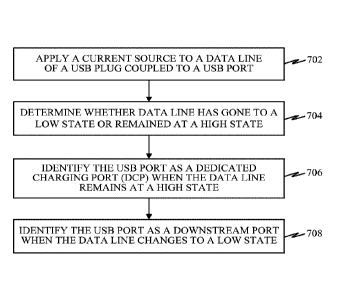
[0048] FIG. 7 is a flow diagram illustrating at least one example of a method
operational on an electronic device, such as the electronic device 104.
Referring to
FIGS. 2, 3, and 7, an electronic device 104 can apply a current source to a
data line of a
USB plug coupled to a USB port at block 702. For example, the processing
circuit 204
(e.g., the charger detector 208) executing the charger detection operations
210 can apply
a current source to a data line of the USB plug. The current source may be a
weak
current source, such as about 10 micro-Amps, as defined by the BC 1.2 spec. In
some
implementations, the current source may be applied to the data line as part of
a
conventional data contact detection (DCD) stage under the BC 1.2 spec. In
other
implementations, the current source may be applied at any other stage of the
BC 1.2
spec, or as its own stage at any placement during the BC 1.2 spec.
[0049] FIG. 8 is a flow diagram depicting at least one example of a process
for
applying the current source to the data line. This process may be implemented
by the
processing circuit 204 as instructed by the charger detection operations 210.
Initially, a
VBUS detect stage is performed, as shown by decision diamond 802. That is, the
processing circuit 204 (e.g., the charger detector 208) executing the charger
detection
operations 210 can detect when the supply voltage (VBUS) has gone high. If the
supply
voltage is not asserted, the process waits until the supply voltage (VBUS) has
been
asserted, which indicates to the electronic device 104 that the USB plug has
been
connected to a port.
[0050] At operation 804, the processing circuit 204 (e.g., the charger
detector 208)
executing the charger detection operations 210 applies a current source to the
data line.
For example, the processing circuit 204 (e.g., the charger detector 208)
executing the
charger detection operations 210 can close the first switch 51 in FIG. 3 of
the charger
detector 208 to apply the current source Idp_src to the data plus line 302.
According to
this example, any pull-down resistor on the other data line is disabled. Thus,
the
processing circuit 204 (e.g., the charger detector 208) executing the charger
detection
operations 210 can ensure that the second switch S2 is open so that the pull-
down
resistor Rdm_dwn on the data minus line 304 is disabled. In another example,
the
processing circuit 204 (e.g., the charger detector 208) executing the charger
detection
12
CA 02926743 2016-04-06
WO 2015/073294
PCT[US2014/064297
operations 210 can apply the current to the data minus line 304, instead of to
the data
plus line 302.
[0051] At operation 806, the processing circuit 204 (e.g., the charger
detector 208)
executing the charger detection operations 210 waits for a data line charging
time. The
data line charging time is a predetermined time period that is adapted to be
sufficiently
long to enable the weak current source to charge capacitance on the data
lines. For
example, the data line charging time may be calculated from the product of the
voltage
and the capacitance divided by the current. Thus, when the voltage is 2 volts,
the
capacitance is 100 picofarads, and the current is 10 microamps, the data line
charging
time would be about 20 microseconds (e.g., 2v x 100pF / 10uA = 20us).
[0052] Returning to the method depicted in the flow diagram in FIG. 7, the
electronic
device 104 can determine whether the data line on which the current source is
applied
has gone to a LOW state or remained at a HIGH state after a predetermined
period of
time, at 704. For example, the processing circuit 204 (e.g., the charger
detector 208)
executing the charger detection operations 210 can monitor the data line on
which the
current source is applied to determine whether the data line remains at a HIGH
state or
whether it goes to a LOW state. In examples where the current source is
applied to the
data line as part of the DCD stage, the processing circuit 204 (e.g., the
charger detector
208) executing the charger detection operations 210 can wait until the timeout
period
has expired.
[0053] FIG. 9 is a flow diagram depicting at least one example of a process
for
determining whether the data line has gone to a LOW state or remained at a
HIGH state.
This process may be implemented by the processing circuit 204 as instructed by
the
charger detection operations 210. At operation 902, the processing circuit 204
(e.g., the
charger detector 208) executing the charger detection operations 210 starts a
timer. In
examples where the current source is applied to the data line as part of the
DCD stage,
the timer can represent the timeout threshold timer (Tdcd_timeout). The timer
at
operation 808, however, may have a duration that extends beyond the 900
millisecond
maximum defined by the BC 1.2 spec for the timeout threshold timer
(Tdcd_timeout).
For example, the timer started at operation 808 may be set with a duration
greater than
900 milliseconds. In at least one example, the timer may be set to a time
duration
selected from within a range of times between 901 milliseconds and 2 seconds.
13
CA 02926743 2016-04-06
WO 2015/073294
PCT[US2014/064297
[0054] At decision diamond 904, the processing circuit 204 (e.g., the charger
detector
208) executing the charger detection operations 210 determines whether the
data line to
which the current source is applied has gone to a LOW state. If the data line
has not
gone to a LOW state, the processing circuit 204 (e.g., the charger detector
208)
executing the charger detection operations 210 can determine whether the timer
has
expired at decision diamond 906. If the timer has not expired, the processing
circuit
204 (e.g., the charger detector 208) executing the charger detection
operations 210
returns to decision diamond 904. On the other hand, if the timer has expired
at decision
diamond 906 and the data line has not gone to the LOW state, then the
processing
circuit 204 (e.g., the charger detector 208) executing the charger detection
operations
210 can determine that the data line is at a HIGH state at operation 908.
[0055] Referring back to FIG. 7, when the data line remains at a HIGH state,
the
electronic device 104 can identify the port as a dedicated charging port
(DCP), at 706.
For example, the processing circuit 204 (e.g., the charger detector 208)
executing the
charger detection operations 210 can identify the USB port to which the USB
plug is
coupled to be a dedicated charging port when the data line remains at a HIGH
state for
the predetermined amount of time while the current source is applied. This
identification will apply to both compliant and non-compliant dedicated
charging ports.
For example, when the electronic device 104 is coupled to the compliant
dedicated
charging port (DCP) 402 depicted in FIG. 4, the data plus line 302 and the
data minus
line 304 in FIG. 3 will remain HIGH due to the pull-down resistor Rdm_dwn
being
disabled. When the electronic device 104 is coupled to the first example of a
non-
compliant dedicated charging port (DCP) 502 in FIG. 5, the data line (either
the data
plus line 302 or the data minus line 304 in FIG. 3, whichever has the current
source
applied thereto) will remain HIGH. Similarly, the data line on which the
current source
is applied will remain HIGH when the electronic device 104 is coupled to the
second
example of a non-compliant dedicated charging port (DCP) 602 in FIG. 6, as a
result of
the data lines floating in the non-compliant dedicated charging port (DCP).
[0056] Turning again to FIG. 9, the data line has gone LOW at decision diamond
904,
then the processing circuit 204 (e.g., the charger detector 208) executing the
charger
detection operations 210 determine that the data line is at a LOW state.
Turning back to
FIG. 7, when the data line changes to a LOW state, the electronic device 104
can
identify the port as a downstream port at block 708. For example, the
processing circuit
14
CA 02926743 2016-04-06
WO 2015/073294
PCT/US2014/064297
204 (e.g., the charger detector 208) executing the charger detection
operations 210 can
identify the USB port to which the USB plug is coupled to be a downstream port
(e.g., a
standard downstream port (SDP) or a charging downstream port (CDP)) if the
data line
changes to a LOW state. In the example where the electronic device 104 is
coupled to a
downstream port (e.g., a standard downstream port (SDP) or a charging
downstream
port (CDP)), a pull-down resistor on the data plus line or a pull-down
resistor on the
data minus line inside the downstream port will cause the data line on which
the current
source is applied to go to a LOW state.
[0057] In various implementations, the steps of 702 through 708 can be
performed as
a data contact detect stage. That is, instead of the electronic device 104
performing a
data contact detect stage, the steps associated with 702 through 708 may be
performed.
In other implementations, a conventional data contact detect stage may be
performed
prior to steps 702 through 708.
[0058] When the port is identified as a downstream port, the electronic device
104 can
further determine whether the downstream port is a standard downstream port
(SDP) or
a charging downstream port (CDP). FIG. 10 is a flow diagram of a method
operational
on an electronic device for determining whether the downstream port is a
standard
downstream port (SDP) or a charging downstream port (CDP). After the
electronic
device has identified the USB port as a downstream port at 708 in FIG. 7, the
electronic
device 104 can remove the current source from the data line and can then apply
a
voltage source to the data plus line 302, at 1002. For example, the processing
circuit
204 (e.g., the charger detector 208) executing the charger detection
operations 210 can
close the third switch S3 so that the voltage source Vdat_src is applied to
the data plus
line 302.
[0059] At 1004, the electronic device 104 can determine whether the data minus
line
304 is LOW or HIGH in response to the voltage source applied to the data plus
line 302.
For example, the processing circuit 204 (e.g., the charger detector 208)
executing the
charger detection operations 210 can set the fourth switch S4 to the data
minus line 304
to compare the voltage on the data minus line 304 to a reference voltage
Vdat_ref in
FIG. 3. If the data minus line 304 is determined to be LOW (e.g., less than
the
reference voltage Vdat_ref), then the processing circuit 204 (e.g., the
charger detector
208) executing the charger detection operations 210 can identify the USB port
as a
standard downstream port (SDP) at 1006. If the data minus line 304 is
determined to be
CA 02926743 2016-04-06
WO 2015/073294
PCT/US2014/064297
HIGH (e.g., greater than or equal to the reference voltage Vdat_ref), then the
processing
circuit 204 (e.g., the charger detector 208) executing the charger detection
operations
210 can identify the USB port as a charging downstream port (CDP) at 1008.
[0060] According to another aspect of the disclosure, electronic devices can
be
adapted to quickly detect whether a charging port is a compliant or non-
compliant (e.g.,
proprietary) charging port. As noted above, a data contact detection (DCD)
stage is
typically employed under the BC 1.2 spec by closing the second switch S2 in
FIG. 3 to
enable the pull-down resistor Rdm_dwn on the data minus line 304, and the
third switch
S3 is closed to apply the current source Idp_src to the data plus line 302 for
a
predetermined period of time. Typically, the BC 1.2 spec defines the
predetermined
period as a Tdcd_timeout timer that is set with a duration between 300
milliseconds and
900 milliseconds.
[0061] If the timeout occurs (e.g., the time period expires without the data
plus line
302 being pulled down by the pull-down resistor Rdm_dwn on the data minus line
304),
the data contact detect stage is typically considered to have failed. It has
been observed
that the non-compliant (e.g., proprietary) dedicated charging ports, such as
those
depicted in FIGS. 5 and 6, result in a timeout of the data contact detection
stage.
Therefore, the electronic device 104 can be adapted to identify the USB port
to which it
is coupled as a non-compliant (or proprietary) dedicated charging port (DCP)
in
response to timeout at the data contact detect stage. In some examples, to
ensure that
there has been sufficient time for the data lines to be put into contact with
the USB port,
the predetermined period (e.g., the Tdcd_timeout timer) can be set to a time
greater than
900 milliseconds. In at least one example, the predetermined period can be set
to a
value between 901 milliseconds and 2 seconds.
[0062] FIG. 11 is a flow diagram illustrating at least one example of another
method
operational on an electronic device, such as the electronic device 104.
Referring to
FIGS. 2, 3, and 11, an electronic device 104 can apply a current source to a
data plus
line of a USB plug coupled to a USB port at 1102. For example, the processing
circuit
204 (e.g., the charger detector 208) executing the charger detection
operations 210 can
close the first switch 51 to apply a current source Idp src to the data plus
line 302.
[0063] At 1104, the electronic device 104 can enable a pull-down resistor on
the data
minus line of the USB plug. For example, the processing circuit 204 (e.g., the
charger
16
CA 02926743 2016-04-06
WO 2015/073294
PCT/US2014/064297
detector 208) executing the charger detection operations 210 can close the
second
switch S2 to enable the pull-down resistor Rdm_dwn on the data minus line 304.
[0064] At 1106, the electronic device 104 can detect that the data plus line
remains at
a HIGH state for a predetermined period of time. For example, the processing
circuit
204 (e.g., the charger detector 208) executing the charger detection
operations 210 can
detect that the data plus line 302 remains at the high state for the duration
of the
Tdcd_timeout timer. As noted above, the Tdcd_timeout timer may be modified
from
the BC 1.2 spec to be greater than 900 milliseconds.
[0065] At 1108, the electronic device 104 can identify the USB port to which
the USB
plug is coupled as a proprietary or non-compliant dedicated charging port
(DCP) in
response to the determination that the data plus line remained at the HIGH
state for the
duration of the predetermined period of time. For example, the processing
circuit 204
(e.g., the charger detector 208) executing the charger detection operations
210 can
indicate the USB port to be a proprietary DCP in response to timeout
occurring.
[0066] The features described herein and associated with FIG. 11 can be
employed
independently from the features described above with reference to FIG. 7. For
example,
the non-compliant charger detection features described herein (e.g., with
reference to
FIG. 11) can be employed with the conventional detection process defined by
the BC
1.2 spec, where failure of the DCD stage can indicate that the port is a non-
compliant
dedicated charging port (DCP). In other examples, the non-compliant charger
detection
features described herein (e.g., with reference to FIG. 11) can be employed in
combination with the dedicated charging port (DCP) detection features
described herein
(e.g., with reference to FIG. 7).
[0067] While the above discussed aspects, arrangements, and embodiments are
discussed with specific details and particularity, one or more of the
components, steps,
features and/or functions illustrated in FIGS. 1, 2, 3, 4, 5, 6, 7, 8, 9, 10,
and/or 11 may
be rearranged and/or combined into a single component, step, feature or
function or
embodied in several components, steps, or functions. Additional elements,
components,
steps, and/or functions may also be added or not utilized without departing
from the
present disclosure. The apparatus, devices and/or components illustrated in
FIGS. 1, 2,
3, 4, 5, and/or 6 may be configured to perform or employ one or more of the
methods,
features, parameters, and/or steps described in FIGS. 7, 8, 9, 10, and/or 11.
The novel
17
CA 02926743 2016-04-06
WO 2015/073294
PCT[US2014/064297
algorithms described herein may also be efficiently implemented in software
and/or
embedded in hardware.
[0068] While features of the present disclosure may have been discussed
relative to
certain embodiments and figures, all embodiments of the present disclosure can
include
one or more of the advantageous features discussed herein. In other words,
while one or
more embodiments may have been discussed as having certain advantageous
features,
one or more of such features may also be used in accordance with any of the
various
embodiments discussed herein. In similar fashion, while exemplary embodiments
may
have been discussed herein as device, system, or method embodiments, it should
be
understood that such exemplary embodiments can be implemented in various
devices,
systems, and methods.
[0069] Also, it is noted that at least some implementations have been
described as a
process that is depicted as a flowchart, a flow diagram, a structure diagram,
or a block
diagram. Although a flowchart may describe the operations as a sequential
process,
many of the operations can be performed in parallel or concurrently. In
addition, the
order of the operations may be re-arranged. A process is terminated when its
operations
are completed. A process may correspond to a method, a function, a procedure,
a
subroutine, a subprogram, etc. When a process corresponds to a function, its
termination corresponds to a return of the function to the calling function or
the main
function. The various methods described herein may be partially or fully
implemented
by programming (e.g., instructions and/or data) that may be stored in a
machine-
readable, computer-readable, and/or processor-readable storage medium, and
executed
by one or more processors, machines and/or devices.
[0070] Those of skill in the art would further appreciate that the various
illustrative
logical blocks, modules, circuits, and algorithm steps described in connection
with the
embodiments disclosed herein may be implemented as hardware, software,
firmware,
middleware, microcode, or any combination thereof. To clearly
illustrate this
interchangeability, various illustrative components, blocks, modules,
circuits, and steps
have been described above generally in terms of their functionality. Whether
such
functionality is implemented as hardware or software depends upon the
particular
application and design constraints imposed on the overall system.
100711 The various features associate with the examples described herein and
shown
in the accompanying drawings can be implemented in different examples and
18
CA 02926743 2016-04-06
WO 2015/073294
PCT/1JS2014/064297
implementations without departing from the scope of the present disclosure.
Therefore,
although certain specific constructions and arrangements have been described
and
shown in the accompanying drawings, such embodiments are merely illustrative
and not
restrictive of the scope of the disclosure, since various other additions and
modifications
to, and deletions from, the described embodiments will be apparent to one of
ordinary
skill in the art. Thus, the scope of the disclosure is only determined by the
literal
language, and legal equivalents, of the claims which follow.
19