Note: Descriptions are shown in the official language in which they were submitted.
- 1 -
LIGHT EMITTING DIODE (LED) DEVICES
BACKGROUND OF THE INVENTION
Field of the Invention
[0001] The present invention relates to display systems comprising light-
emitting
diodes (LEDs), suitably blue light LEDs, which demonstrate increased optical
power output. In embodiments, the display systems include compositions
comprising phosphors, including luminescent nanocrystals.
Background of the Invention
[0002] In liquid crystal display (LCD) backlights, white LEDs are
typically utilized
as a light source. In one configuration, the LEDs are arranged around the edge
or perimeter of the display. In such the case of edge-lit backlights, light
emanating from the LEDs enters a light guide plate which distributes white
light uniformly across the display. White LED package designs have been
optimized to enable high extraction efficiency and coupling efficiency into
the
light guide plate.
[0003] LCD backlights often utilize phosphors, such as YAG phosphors.
Traditionally, these phosphors have been situated inside the LED package
itself.
Luminescent nanocrystals represent a new, alternative class of phosphors often
used in remote-phosphor configurations where the phosphor is no longer inside
the LED package. For example, luminescent nanocrystals can be embedded in
a flexible film/sheet that is placed above a light guide plate (see, e.g.,
Published
U.S. Patent Application Nos. 2010/0110728 and 2012/0113672). In other
examples, luminescent nanocrystals are encapsulated in a container, for
example a capillary, which is placed between the LEDs and the light guide
plate
(see, e.g., Published U.S. Patent Application No 2010/0110728).
Date Recue/Date Received 2021-04-28
-2-
100041 Blue LED light extraction efficiency and coupling efficiency into
the light guide
plate play a critical role in the overall display efficiency. Blue light
extraction efficiency
is poor in current blue LED designs. This is most likely a result of the
reflection from the
encapsulation-polymer/air interface. A significant amount of the blue light is
reflected
from this interface back toward the blue die of the LED, which in turn absorbs
the blue
light.
[0005] Disclosed herein are embodiments that overcome this deficiency with
blue LED-
based display devices, thereby increasing the optical power output of such
devices.
SUMMARY OF PREFERRED EMBODIMENTS
[0006] In embodiments, the present application provides display systems,
suitably
comprising one or more blue light emitting diode(s) (LED), a light guide
plate, optically
coupled to the blue LED, a display and a composition comprising a plurality of
phosphors, the composition oriented between the light guide plate and the
display.
Suitably, the display system exhibits increased optical power output as
compared to a
display system where the light guide plate is not optically coupled to the
blue LED.
[0006a] Also provided is a method of providing a display system, the method
comprising:
disposing an optically clear material between one or more blue light emitting
diodes
(LEDs) and a light guide plate to eliminate an air gap between the one or more
blue
LEDs and the light guide plate, and to optically couple the one or more blue
LEDs to the
light guide plate, the optically clear material having a refractive index
matched to the
light guide plate to reduce optical losses of light passing between the one or
more blue
LEDs and the light guide plate during operation; providing a display panel,
such that light
provided by the one or more blue LEDs associated with the display system can
pass
through the optically clear material and the light guide plate to the display
panel; and
disposing a composition comprising a plurality of nanocrystal phosphors
oriented
CA 2927191 2019-10-15
- 2a -
between the light guide plate and the display panel; wherein, when light is
provided from
the one or more blue LEDs through the optically clear material and the light
guide plate,
the display system exhibits increased optical power output due at least in
part to the
elimination of the air gap by the optically clear material.
[0006b] Also provided is a method of providing a display system, the method
comprising:
providing a light source, the light source comprising one or more blue light
emitting
diodes (LEDs) having a clear encapsulation polymer; disposing an optically
clear
material between the light source and a light guide plate to eliminate an air
gap between
the light source and the light guide plate, and to optically couple the light
source to the
light guide plate, the optically clear material having a refractive index
matched to the
light guide plate to reduce optical losses of light passing between the light
source and the
light guide plate during operation; providing a display panel, such that light
provided by
the light source associated with the display system can pass through the
optically clear
material and the light guide plate to the display panel; and providing a
composition
comprising a plurality of nanocrystal phosphors, the composition oriented
between the
light guide plate and the display panel; wherein, when light is provided from
the light
source through the optically clear material and the light guide plate, the
display system
exhibits increased optical power output due at least in part to the
elimination of the air
gap by the optically clear material.
[0007] In embodiments, the light guide plate is optically coupled to the
blue LED with a
tape or an adhesive. In embodiments, the light guide plate is optically
coupled to the blue
LED via an encapsulant protruding from the LED.
[0008] Suitably, the phosphors are YAG phosphors, silicate phosphors,
garnet phosphors,
aluminate phosphors, nitride phosphors, NYAG phosphors, SiAlON phosphors and
CASN phosphors. In further embodiments, the phosphors are luminescent
nanocrystals,
for example luminescent nanocrystals comprising CdSe or ZnS, including for
example,
luminescent nanocrystals comprising CdSe/ZnS, InP/ZnS, InP/ZnSe, PbSe/PbS,
CdSe/CdS, CdTe/CdS or CdTe/ZnS.
[0009] In exemplary embodiments, the composition is a film.
CA 2927191 2019-10-15
CA 02927191 2016-04-12
- 3 -
[00010] Suitably, the display is a liquid crystal module.
[00011] In additional embodiments, the systems further comprise one or more
of a
diffuser, one or more brightness enhancement films (BEFs) and a reflector.
[00012] In embodiments, the display systems suitably exhibit at least a 10%
increase
in optical power output as compared to a display system where the light guide
plate
is not optically coupled to the blue LED.
[00013] Also provided are display systems, suitably comprising one or more
blue
light emitting diode(s) (LED), a light guide plate optically coupled to the
blue LED,
a display and a film comprising a plurality of phosphors, the film oriented
between
the light guide plate and the display. Suitably, the display system exhibits
at least a
10% increase in optical power output as compared to a display system where the
light guide plate is not optically coupled to the blue LED.
[00014] Exemplary methods for optical coupling are described herein, as are
suitable
phosphors, including luminescent nanocrystals.
[00015] Also provided are display systems, suitably comprising one or more
blue
light emitting diode(s) (LED), a light guide plate, optically coupled to the
blue LED,
a polymeric film comprising a plurality of phosphors, the polymeric film
oriented
above the light guide plate, one or more brightness enhancement films (BEFs)
oriented above the polymeric film, a top diffuser oriented above the BEFs and
a
liquid crystal module oriented above the top diffuser. Suitably, the display
systems
exhibit at least a 10% increase in optical power output as compared to a
display
system where the light guide plate is not optically coupled to the blue LED.
[00016] Exemplary methods for optical coupling are described herein, as are
suitable
phosphors, including luminescent nanocrystals.
[00017] Also provided are methods of increasing optical power output of a
blue light
emitting diode (LED) in a display system, comprising optically coupling the
blue
LED to a light guide plate of the display system.
-4-
1000181 In embodiments of the methods, the optical coupling comprises
coupling the
blue LED to the light guide plate with tape or an adhesive. In embodiments of
the methods, the light guide plate is optically coupled to the blue LED via an
encapsulant protruding from the LED.
[00019] Suitably, the methods increase the optical power output of the blue
LED by
at least 10% as compared to a display system that does not comprise the blue
LED optically coupled to the light guide.
[00020] Further embodiments, features, and advantages of the embodiments,
as well
as the structure and operation of the various embodiments, are described in
detail below with reference to accompanying drawings.
BRIEF DESCRIPTION OF THE FIGURES
[00021] FIG. lA shows an exemplary display system as described herein.
[00022] FIG. 1B shows an additional exemplary display system as described
herein.
[00023] FIGs. 2A-2C show schematics illustrating the source of loss of
optical power
output in blue LEDs and the effect of optical coupling between an LED and a
light guide plate.
[00024] FIGs. 3A-3B show theoretical calculations of spectral power density
and
integrated spectral power density for blue and white LEDs.
[00025]
DETAILED DESCRIPTION OF PREFERRED EMBODIMENTS
[00026] It should be appreciated that the particular implementations shown
and
described herein are examples and are not intended to otherwise limit the
scope
of the application in any way.
[00027]
[00028] As used in this specification, the singular forms "a," "an" and
"the"
specifically also encompass the plural forms of the terms to which they refer,
Date Recue/Date Received 2021-04-28
- 5 -
unless the content clearly dictates otherwise. The term "about" is used herein
to
mean approximately, in the region of, roughly, or around. When referring to
any numerical value, "about" means a value of +/-10% of the stated value (e.g.
"about 100 nm" encompasses a range of sizes from 90 nm to 110 nm,
inclusive).
[00029] Technical and scientific terms used herein have the meaning
commonly
understood by one of skill in the art to which the present application
pertains,
unless otherwise defined. Reference is made herein to various methodologies
and materials known to those of skill in the art.
Luminescent Nanocrystal Phosphors
[00030] Described herein are various compositions comprising nanocrystals,
including luminescent nanocrystals. The various properties of the luminescent
nanocrystals, including their absorption properties, emission properties and
refractive index properties, can be tailored and adjusted for various
applications. As used herein, the term "nanocrystal" refers to nanostructures
that are substantially monocrystalline. A nanocrystal has at least one region
or
characteristic dimension with a dimension of less than about 500 nm, and down
to on the order of less than about 1 nm. The terms "nanocrystal," "nanodot,"
"dot," "quantum dot" and "QD" are readily understood by the ordinarily skilled
artisan to represent like structures and are used herein interchangeably. The
present invention also encompasses the use of polycrystalline or amorphous
nanocrystals. As used herein, the term "nanocrystal" also encompasses
"luminescent nanocrystals." As used herein, the term "luminescent
nanocrystals" means nanocrystals that emit light when excited by an external
energy source (suitably light).
[00031] The material properties of nanocrystals can be substantially
homogenous, or
in certain embodiments, can be heterogeneous. The optical properties of
nanocrystals can be determined by their particle size, chemical or surface
composition. The ability to tailor the luminescent nanocrystal size in the
range
Date Recue/Date Received 2021-04-28
- 6 -
between about 1 nm and about 15 nm enables photoemission coverage in the
entire optical spectrum to offer great versatility in color rendering.
Particle
encapsulation offers robustness against chemical and UV deteriorating agents.
[00032] Nanocrystals, including luminescent nanocrystals, for use in
embodiments
described herein can be produced using any method known to those skilled in
the art. Suitable methods and exemplary nanocrystals are disclosed in U.S.
Patent No. 7,374,807; U.S. patent application Ser. No. 10/796,832, filed Mar.
10, 2004; U.S. Pat. No. 6,949,206; and U.S. Provisional Patent Application No.
60/578,236, filed Jun. 8, 2004.
[00033] Luminescent nanocrystals for use in embodiments described herein
can be
produced from any suitable material, including an inorganic material, and more
suitably an inorganic conductive or semiconductive material. Suitable
semiconductor materials include those disclosed in U.S. patent application
Ser.
No. 10/796,832, and include any type of semiconductor, including group II-VI,
group III-V, group IV-VI and group IV semiconductors. Suitable
semiconductor materials include, but are not limited to, Si, Ge, Sn, Se, Te,
B, C
(including diamond), P, BN, BP, BAs, MN, AlP, AlAs, AlSb, GaN, GaP,
GaAs, GaSb, InN, InP, InAs, InSb, MN, AlP, AlAs, AlSb, GaN, GaP, GaAs,
GaSb, ZnO, ZnS, ZnSe, ZnTe, CdS, CdSe, CdTe, HgS, HgSe, HgTe, BeS,
BeSe, BeTe, MgS, MgSe, GeS, GeSe, GeTe, SnS, SnSe, SnTe, Pb0, PbS,
PbSe, PbTe, CuF, CuCl, CuBr, CuI, Si3N4, Ge3N4, A1203, (Al, Ga, In)2 (S, Se,
Te)3, Al2CO3 and an appropriate combination of two or more such
semiconductors.
[00034] In certain embodiments, the nanocrystals may comprise a dopant from
the
group consisting of a p-type dopant or an n-type dopant. The nanocrystals
useful herein can also comprise II-VI or III-V semiconductors. Examples of II-
VI or III-V semiconductor nanocrystals include any combination of an element
from Group II, such as Zn, Cd and Hg, with any element from Group VI, such
as S, Se, Te and Po, of the Periodic Table; and any combination of an element
Date Recue/Date Received 2021-04-28
- 7 -
from Group III, such as B, Al, Ga, In, and Ti, with any element from Group V,
such as N, P, As, Sb and Bi, of the Periodic Table.
[00035] The nanocrystals, including luminescent nanocrystals, useful in
embodiments described herein can also further comprise ligands conjugated,
cooperated, associated or attached to their surface. Suitable ligands include
any
group known to those skilled in the art, including those disclosed in U.S.
patent
application Ser. No. 12/799,813, filed April 29, 2010; U.S. patent application
Ser. No. 12/076,530, filed Mar. 19, 2008; U.S. patent application Ser. No.
12/609,736, filed Oct. 30, 2009; U.S. patent application Ser. No. 11/299,299,
filed Dec. 9, 2005; U.S. Pat. No. 7,645,397; U.S. Pat. No. 7,374,807; U.S.
Pat.
No. 6,949,206; U.S. Pat. No. 7,572,393; and U.S. Pat. No. 7,267,875. Use of
such ligands can enhance the ability of the nanocrystals to incorporate into
various solvents and matrixes, including polymers. Increasing the miscibility
(i.e., the ability to be mixed without separation) of the nanocrystals in
various
solvents and matrixes allows them to be distributed throughout a polymeric
composition such that the nanocrystals do not aggregate together and therefore
do not scatter light. Such ligands are described as "miscibility-enhancing"
ligands herein.
[00036] In certain embodiments, compositions comprising nanocrystals
distributed or
embedded in a matrix material are provided. Suitable matrix materials can be
any material known to the ordinarily skilled artisan, including polymeric
materials, organic and inorganic oxides. Compositions described herein can be
layers, encapsulants, coatings, sheets or films. It should be understood that
in
embodiments described herein where reference is made to a layer, polymeric
layer, matrix, sheet or film, these terms are used interchangeably, and the
embodiment so described is not limited to any one type of composition, but
encompasses any matrix material or layer described herein or known in the art.
[00037] Down-converting nanocrystals (for example, as disclosed in U.S.
Patent No.
7,374,807) utilize the emission properties of luminescent nanocrystals that
are
tailored to absorb light of a particular wavelength and then emit at a second
Date Recue/Date Received 2021-04-28
- 8 -
wavelength, thereby providing enhanced performance and efficiency of active
sources (e.g., LEDs).
[00038] While any method known to the ordinarily skilled artisan can be
used to
create nanocrystals (luminescent nanocrystals), suitably, a solution-phase
colloidal method for controlled growth of inorganic nanomaterial phosphors is
used. See Alivisatos, A. P., "Semiconductor clusters, nanocrystals, and
quantum
dots," Science 271:933 (1996); X. Peng, M. Schlamp, A. Kadavanich, A. P.
Alivisatos, "Epitaxial growth of highly luminescent CdSe/CdS Core/Shell
nanocrystals with photostability and electronic accessibility," I Am. Chem.
Soc.
30:7019-7029 (1997); and C. B. Murray, D. J. Norris, M. G. Bawendi,
"Synthesis and characterization of nearly monodisperse CdE (E=sulfur,
selenium, tellurium) semiconductor nanocrystallites," J Am. Chem. Soc.
115:8706 (1993). This manufacturing process technology leverages low cost
processability without the need for clean rooms and expensive manufacturing
equipment. In these methods, metal precursors that undergo pyrolysis at high
temperature are rapidly injected into a hot solution of organic surfactant
molecules. These precursors break apart at elevated temperatures and react to
nucleate nanocrystals. After this initial nucleation phase, a growth phase
begins
by the addition of monomers to the growing crystal. The result is freestanding
Date Recue/Date Received 2021-04-28
CA 02927191 2016-04-12
WO 2015/057930
PCT/US2014/060840
- 9
crystalline nanopartieles in solution that have an organic surfactant molecule
coating their surface.
[00039] Utilizing this approach, synthesis occurs as an initial nucleation
event
that takes place over seconds, followed by crystal growth at elevated
temperature for several minutes. Parameters such as the temperature,, types of
surfactants present, precursor materials, and ratios of sutfactants to
monomers
can be modified so as to change the nature and progress of the reaction. The
temperature controls the structural phase of the nucleation event, rate of
decomposition of precursors, and rate of growth. The organic surfactant
molecules mediate both solubility and control of the nanocrystal shape. The
ratio of surfactants to monomer, surfactants to each other, monomers to each
other, and the individual concentrations of monomers strongly influence the
kinetics of growth.
100040] In suitable embodiments, CdSe is used as the nanocrystal material,
in
one example. for visible light down-conversion, due to the relative maturity
of
the synthesis of this material. Due to the use of a generic surface chemistry,
it
is also possible to substitute non-cadmium-containing nanocrystals.
Core/Shell Luminescent .Nanocrystals
100041] In semiconductor nanocrystals, photo-induced emission arises from
the
band edge states of the nanocrystal. The band-edge emission from luminescent
nanocrystals competes with radiative and non-radiative decay channels
originating from surface electronic states. X. Peng, el al., 1 Am. Chem. Soc.
30:7019-7029 (1997). As a result, the presence of surface defects such as
dangling bonds provide non-radiative recombination centers and contribute to
lowered emission efficiency. An efficient and permanent method to passivate
and remove the surface trap states is to epitaxially grow an inorganic shell
material on the surface of the nanocrystal. X. .Peng, el at., J. Am. Chem.
Soc.
30:7019-7029 (1997). The shell material can be chosen such that the electronic
levels are type I with respect to the core material (e.g., with a larger
bandgap
CA 02927191 2016-04-12
WO 2015/057930
PCT/US2014/060840
0 -
to provide a potential step localizing the electron and hole to the core). As
a
result, the probability of non-radiative-recombination can be reduced.
[00042J Core-shell structures are obtained by adding organometallie
precursors
containing the shell materials to a reaction mixture containing the core
nanocrystal. In this case, rather than a nucleation event followed by .growth,
the cores act as the nuclei, and the shells grow from their surface. The
temperature of the reaction is kept low to favor the addition of shell
material
monomers to the core surface, while preventing independent nucleation of
nanocrystals -of the shell materials. Surfactants in the reaction mixture are
present to direct the controlled growth of shell material and to ensure
solubility. A uniform and epitaaially grown shell is obtained when there is a
low lattice mismatch between the two materials.
1000431 Exemplary materials for preparing core-shell luminescent
nanocrystals
include, but are nor limited to, Si,- Ge, Sn, Se, Te, 13, C (including
diamond), P,
Co, Au, EN, BP, BAs, MNõ A1P, ALAs, AlSh, GaN, GaP, GaAs, GaSh, InN,
InAs, InSh, MN, MP, AlAsõAlSb, GaN, GaP, GaAs, GaSb, 7.40, ZaS,
ZnSe, ZnTe, CdS, CdSe, CdTe, FIgS, figSe, HgTe, BeS, BeSe, BeTe, NUS,
MgSe, GeSõ GeSe, GeTe, SnS, SnSe, Sae, MO, PbS, PbSeõ PbTe, C.uF,
Cala, Cali., Cul, S13N4, Ge3b14, A1203, (Al, Ga, In)3 (S, Sc, Te)3, AlCO, and
an appropriate combination of two or more such materials. Exemplary core-
shell luminescent nanocrystals for use in the practice of the present
invention
include, but are not limited toõ (represented as Core/Shell)õ CdSeanS,
InPIZnS, InP/ZnSe, PhSe/PbS, CdSe/CdS, CdTe/CdS, CciTeanS, as well as
others.
[000441 As used throughout, a plurality of phosphors or a plurality of
luminescent nanocrystals means more than one phosphor or luminescent
nanocrystal (i.e., 2, 3, 4, 5, 10, 100, 1,000, 1,000,000, etc., nanocrystals).
The
compositions will suitably comprise phosphors or luminescent nanocrystals
having the same composition, though in further embodiments, the plurality of
phosphors or luminescent nanocrystals can be various different. compositions.
For example, the luminescent nanocrystals can all emit at the same
CA 02927191 2016-04-12
WO 2015/057930
PCT/US2014/060840
H -
wavelength, or in further embodiments, the compositions can comprise
luminescent nanocrystals that emit at different wavelengths.
1009451 Luminescent nanocrystals for use in the embodiments described
herein
will suitably be less than about 100 am in size, and down to less than about 2
mu in size. in suitable embodiments, the luminescent nanocrystals of the
present invention absorb visible light. As used herein, visible, light is
electromagnetic radiation with wavelengths between about 380 and about 780
nanometers that is visible to the human eye. Visible light can be separated
into
the various colors of the spectrum, such as red, orange, yellow, green, blue,
indigo and violet As used herein, blue light comprises light between about
435 mu arid about SOO rim, green light comprises light between about 520 rim
and 565 am and red light comprises light between about 625 am and about
740 um in wavelength.
[00046j in embodiments, the luminescent nanocrystals have a size and a.
composition such that they absorb photons that are in the ultraviolet, near-
infrared, and/or infrared spectra. As used herein, the ultraviolet spectrum
comprises light between about 100 nin to about 400 rim, the near-infrared
spectrum comprises light between about 750 Tim to about 100 pin in
wavelength and the infrared spectrum comprises light between about 750 mu
to about 300 j.tm in wavelength.
f000471 While luminescent nanocrystals of any suitable material can be used
in
the various embodiments described herein, in certain embodiments, the
nanocrystals can be ZaS, InAs or CdSe nanocrystals, or the nanocrystals can
comprise various combinations to form a population of nanocrystais for use in
the practice of the present invention. As discussed above, in further
embodiments, the luminescent nanocrystals are core/shell nanocrystals, such
as CdSe/ZnS, [TIP/We, CdSeCdS or InP/ZnS.
[000481 In embodiments, the luminescent nanocrystals will include at least
one
population of luminescent nanocrystals capable of emitting red light and at
least one population of luminescent nanocrystals capable of emitting green
light upon excitation by a blue light source. The luminescent nanocryStal
- 12 -
wavelengths and concentrations can be adjusted to meet the optical performance
required. In still other embodiments, the luminescent nanocrystals phosphor
material can comprise a population of luminescent nanocrystals which absorb
wavelengths of light having undesirable emission wavelengths, and reemit
secondary light having a desirable emission wavelength. In this manner, the
luminescent nanocrystal films described herein comprise at least one
population of
color-filtering luminescent nanocrystals to further tune the lighting device
emission and to reduce or eliminate the need for color filtering.
[00049] Suitable luminescent nanocrystals, methods of preparing luminescent
nanocrystals, including the addition of various solubility-enhancing ligands,
can be
found in Published U.S. Patent Application No. 2012/0113672.
Display Systems
[00050] In embodiments, various display systems are provided herein that
are
suitably used in any number of applications. As used herein, a "display
system"
refers an arrangement of elements that allow for the visible representation of
data
on a display. Suitable displays include various flat, curved or otherwise-
shaped
screens, films, sheets or other structures for displaying information visually
to a
user. Display systems described herein can be included in, for example,
devices
encompassing a liquid crystal display (LCD), televisions, computers, mobile
phones, smart phones, personal digital assistants (PDAs), gaming devices,
electronic reading devices, digital cameras, and the like.
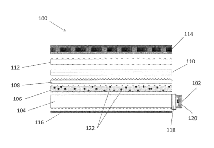
[00051] An exemplary display system 100 is shown in FIG. 1A. In
embodiments,
display system 100 comprises one or more blue light emitting diode(s) (LED)
102. Various orientations and components of LEDs are well known to those of
ordinary skill in the art. Blue LEDs described herein suitably emit in the
range of
440-470 nm. For example, the blue LEDs can be
Date Recue/Date Received 2021-04-28
CA 02927191 2016-04-12
WO 2015/057930
PCT/US2014/060840
- 13 -
GaN LEDs such as a GaN LED which emits blue light at a wavelength of 450
nm.
1000521 As shown in FIG. 1A, display system 100 also comprises light guide
plate 104. Suitably, light guide plate .104 is optically coupled to the one or
more blue LEDs in the display systems described throughout.
100053i As used herein the following terms are used interchangeably, "light
guide plate," "light guide," or "light guide panel," and refer to an optical
.component that is suitable for directing electromagnetic radiation (light)
from
one position to another. Exemplary light guide plates include fiber optic
cables, polymeric or glass solid bodies such as plates, films, containers, or
other structures. The size of the light guide plate will depend on the
ultimate
application and characteristics of the LED. In general,. the thickness of the
light guide plate will be compatible with thickness of the LED.. The other
dimensions of the light guide plate are generally designed to extend beyond
the dimensions of the LED, and are suitably on the order of IOs of
millimeters,
to lOs to 1008 of centimeters. While the light guide plates illustrated in the
Figures represent embodiments suitable for use. in display systems and the
like, other light guides, including fiber optic cables, etc., can also be
utilized.
(000541 Suitable light guide plate materials include polycarbonate (PC),
poly
methyl methacrylate (PMMA), methyl methacrylate, styrene, acrylic polymer
resin, glass, or any suitable light guide plate materials known in the art.
Suitable manufacturing methods for the light guide plate include injection
molding, extrusion, or other suitable embodiments known in the an. In
exemplary embodiments, the light guide plate provides uniform primary light
emission from the top surface of the light guide plate, such that primary
light
entering the luminescent nanoorystal film is of uniform color and brightness.
The light guide plate can include.any thickness or shape known in the art. For
example, the light guide plate thickness can be uniform over the entire light
guide plate surface. Alternatively, the light guide plate can have a wedge-
like
shape.
CA 02927191 2016-04-12
WO 2015/057930
PCT/US2014/060840
- 14 -
[000551 As used herein,
"optically coupled" means that components (e.g., a
fight guide plate and an LED) are positioned so that light is able to pass
from
one component. to another component without substantial interference. Optical
coupling includes embodiments in which components such as a light guide
plate and an LED are in direct physical contact, or as shown in FIG. IA, the
light guide plate '104 and the LED 102 are each in contact with an optically
transparent element I The optically
transparent element may comprise tape
or adhesive, including various glues, polymeric compositions such as
silicones, etc. placed between the light guide plate 104 and the LED 102 to
optically couple the elements. Additional optically transparent adhesives that
can be used in embodiments described herein include various polymers,
including, but not limited to, poly(vinyl butyral)zpoly(vinyl acetate);
epoxies;
urethanes; silicone and derivatives of silicone, including, but not limited
to,
polyphenylmethylsiloxane, pointhenylalkylsiloxane, polydiphenylsiloxane,
polydialkylsilexaneõ fluorinated silicones and vinyl and hydride substituted
silicones; acrylic polymers and copolymers formed from monomers including,
but not limited to, methylmetbacrylate, butylmethacrylate and
laurylmethacrylate; styrene based polymers; and polymers that are cross
linked with difunctional monomers, such as divinylbenzene.
1000%1 In further embodiments, optical coupling can be accomplished,
for
example, by utilizing a polymeric light guide plate, that when heated, melts
or
deforms such that an LED can be contacted to the light guide plate, and then
the light guide plate cooled, thereby facilitating the formation of a physical
adhesion or contact between the two elements. In further embodiments,
optical coupling can be achieved with blue LEDs that have an encapsulant
protruding from The LED, for example a protruding polymer surface filled
with a compliant encapsulation polymer having a refractive index similar to
the refractive index of the light guide plate. In such embodiments, when the
light guide plate is pressed against the blue LED, an optical coupling is
formed
directly between the light guide plate and the LED via the protruding
encapsulant, i.e., the encapsulation polymer.
CA 02927191 2016-04-12
WO 2015/057930
PCT/US2014/060840
- 15 -
1000571 It should he noted that while optical coupling does not require
physical
interaction between the components, suitably physical interaction does occur,
and suitably involves contact and is facilitated by an adhering composite
(e.g.,
tape or polymer) connecting the two components. So long as light is able to
pass between the components they are considered optically coupled.
[00058} Display system 100. shown in FIG. IA, also suitably further
comprises
a display, for example, liquid. crystal module 114. As used herein, the
"display" or "display panel" of the display systems is the portion of the
display
output seen by the user or observer of the display systems.
1000.591 Display system 100 also suitably further comprises composition 106
comprising a plurality of phosphors 122, the composition oriented between the
light guide plate and the display. As described herein, in embodiments,
display system 100 exhibits increased optical power output as compared to a
display system where the light .guide plate is not optically coupled to the
blue
LED.
1000601 in embodiments, the display systems described herein suitably
comprise one or more additional elements traditionally found in LED-based
display systems. Such elements, as shown in FIG. IA, include, but are not
limited to, one or more of diffuser(s) 112 (top or bottom), horizontal
brightness enhancement film(s) (BEF) 110, vertical BEE(s) 108, and
reflector(s) 116. Suitably orientations of these elements, their manufacture
and incorporation in display systems are well known in the art.
1000611 Diffusers, or diffuser films, are distinct from and supplemental to
the
scattering features described herein. Diffusers 112 can include any diffuser
film known in the art, including gain diffuser films, and can be disposed
above
or below the one or more BEFs 108, 110 or other optical films of the display
systems. In exemplary embodiments, the composition comprising phosphors
(suitably a film comprising luminescent nanocrystals) eliminates the need for
a
conventional bottom diffuser film in the display systems, thereby minimizing
the thickness of the lighting device. The compositions comprising phosphors
can also include one or more scattering or diffitser features associated
CA 02927191 2016-04-12
WO 2015/057930
PCT/US2014/060840
- 16 -
therewith, which can serve the purpose of traditional diffusers in addition to
increasing secondary emission of the phosphors in the compositions.
1000621 The BEFs and brightness enhancing features can include reflective
andlor refractive films, reflective polarizer films, prism films, groove
films,
moved prism films, prisms, pitches, grooves, or any suitable BEFs or
brightness enhancement features known in the art For example, the BEFs can
include conventional BEFs such as Vikuitimi. BE,Fs available from 3hem.
1000631 In exemplaty embodiments, the display systems comprise at least one
REF, more suitably at least two BEFs. Suitably, the display systems can
comprise at least three BEFs. In exemplary embodiments, at least one BEF
comprises a reflective polarizer BEF, e.g., for recycling light which would
otherwise he absorbed by the bottom polarizer film. The brightness-enhancing
features and BEFs can include reflectors and/or refractors, polarizers,
reflective polarizers, light extraction features, light recycling features, or
any
brightness-enhancing features known in the art. The BEFs and brightness-
enhancing features can include conventional .BEFs. For example, the BEN can
include a first layer having pitches or prisms having a first pitch angle, and
at
least a second layer having pitches or prisms having a second pitch angle.
1000641 Reflectors 116 are suitably positioned so as to increase the amount
of
light that is emitted from. the light -guide plate. Reflectors can comprise
any
suitable material, such as a reflective mirror, a film of reflector particles,
a
reflective metal Mtn, or any suitable conventional reflectors. In embodiments,
reflectors are suitably a white film In certain embodiments, the reflectors
can
comprise additional functionality or features, such as scattering, diffuser,
or
brightness-enhancing features.
1000651 In still further embodiments, as shown in Ha 1A, the display
systems
comprise one or more blue LED 102, light guide plate 104, optically coupled
to blue LED 102, a display (e.g., liquid crystal module 114) and a film (e.g.,
106) comprising a plurality of phosphors (122), the composition oriented
between the light guide plate and the liquid crystal module. Suitably, the
display systems described herein exhibit increased optical power output and
CA 02927191 2016-04-12
WO 2015/057930
PCT/US2014/060840
17 -
luminous output as compared to a display system where the light guide plate is
not optically coupled to the blue LED.
[00066i As used herein,
when describing elements of the various display
systems provided, "oriented between" is meant to indicate that various
elements are positioned relative to one another such that. one element, e.g.,
a
composition comprising phosphors, is above one element, but below another,
in a configuration in which the elements arc in a stack or layered
orientation.
It should be understood that other orientations can be utilized in the
embodiments described herein, and can be readily determined by a person of
ordinary skill in the art.
1000671 Exemplary tapes
and adhesives .for optically coupling light guide 104
to blue LED 102 are described herein. In additional embodiments., the blue
LED is coupled to the light guide via an encapsulant protruding from the LED.
In addition, exemplary phosphors, including various luminescent nanocrystals
are described throughout.
1000681 As described
herein, in suitable embodiments, film 106 is a polymeric
film, comprising luminescent nanocrystals. Exemplary polymers for use hi
preparing film 106, and methods of preparing polymeric films comprising
luminescent nanoerystals are described herein.
100069) Additional
elements that can be. included in display systems described
herein are described throughout.
1000701 In an additional embodiment of display system 100, shown in
FIG. IA,
described herein are display systems comprising one or more blue LED 102, a
light guide plate, optically coupled to the blue LED 104, a polymeric film
(e.g., 106) comprising a plurality of phosphors (122), the polymeric film
oriented above the light guide plate 104, a. vertical BEE
108 oriented
above the polymeric film, a horizontal REF 110 oriented above the vertical
REF 108, a top diffuser 112 oriented above the horizontal 13E1'110, and a
liquid crystal module 114 oriented above the top diffuser 112.
[0007.1] Suitably, the
display systems described herein exhibit increased optical
power output as compared to a display system where the light guide plate is
CA 02927191 2016-04-12
WO 2015/057930
PCT/US2014/060840
- 18 -
not optically coupled to the blue LED. In embodiments, display systems
described herein exhibit an optical power output of at least 26 tuW/LED, more
suitably at least 28 inWiLED, or at least 29 InWILED at a driving current of
20 mA.
1000721 Exemplary methods and compositions for preparing the optical
coupling are described herein, as arc exemplary phosphors including
luminescent nanocrystals.,
(000731 'The display systems described herein can comprise one or more
medium materials between adjacent elements of the systems. The system can
include one or more medium material disposed between any of the adjacent
elements in the systems, including the LED and the light guide plate; the
light
guide plate and the composition comprising phosphors; between any different
layers or regions within the composition comprising phosphors; the
composition comprising phosphors and one or more barrier layers; the
composition comprising phosphors and the light guide plate; the composition
comprising phosphors and one or more BEE, diffuser, reflector, or other
features; and between multiple barrier layers, or between any other elements
of the display systems. The one or more media can include any suitable
materiaK including, but not limited to, a vacuum, air, gas, optical materials,
adhesives, optical adhesives, glass, polymers. solids, liquids, gels, cured
materials, optical coupling materials, index-matching or index-mismatching
materials, index-gradient materials, cladding or anti-cladding materials,
spacers, epoxy, silica gel, silicones, any matrix materials described herein,
brightness-enhancing materials, scattering or diffuser materials, reflective
or
anti-reflective materials, wavelength-selective materials, wavelength-
selective
anti-reflective materials, color filters, or other suitable media known in the
an.
Suitable media materials include optically transparent, non-yellowing,
pressure-sensitive optical adhesives. Suitable materials include silicones,
silicone gels, silica gel, epoxies (e.g., Loctitemi Epoxy E-30CL), acrylates
(e.g,, 3MTm Adhesive 2175), and matrix materials mentioned heath'. The one
or more media materials can be applied as a curable. gel or liquid and cured
CA 02927191 2016-04-12
WO 2015/057930
PCT/US2014/060840
during or after deposition, or pre-formed and pm-cured prior to deposition.
Suitable curing methods include UV curing, thermal curing, chemical curing,
or other suitable curing methods known in the art, Suitably, index-matching
media materials can be chosen to minimize optical losses between elements of
the lighting device,
1000741 In additional embodiments, display systems are provided in which a
container comprising a plurality of phosphors is optically coupled to a blue
LED. For example, as shown in display system. 160 in FIG. B. blue LED
162 is optically coupled at 18Z to container 178 that contains a plurality of
phosphors 184, for example a plurality of luminescent nanocrystals as
disclosed herein. In exemplary embodiments, container 178 is a capillary, as
described throughout
1000751 As shown in FIG. 1B, light guide plate 164 is optically coupled to
container 178 at 182, via glue, mechanical alignment alone, various adhesives
as described throughout, or the like, and combinations thereof This can also
be accomplished, for example, by utilizing a polymeric light guide plate, that
when heated, melts or deforms such that hermetically sealed container can be
contacted to the light guide plate, and then the light guide plate cooled,
thereby facilitating the formation of' a physical adhesion or contact between
elements (e.g., between LED, light guide plate and container comprising
phosphors). In additional embodiments, the blue LED is coupled to the light
guide via an encapsulant protruding from the LED,
1000761 In exemplary embodiments, display systems 160 as shown in FIG. 111,
can further comprise bottom diffuser 166 oriented above light guide plate 164,
vertical .BEF 168 oriented above bottom diffuser 166, horizontal BEE 170
oriented above vertical. BEF 168, top diffuser 172 oriented above horizontal
REF 170, and liquid crystal module 174 (i.e., display) oriented above top
diffuser 172. The display systems can also further comprise reflector 176, as
described herein.
- 20 -
Compositions of Phosphors
[00077] As
used herein, the term "phosphors" refers to a synthetic fluorescent or
phosphorescent substance. Exemplary phosphors include traditional materials
such as cerium(II)-doped YAG phosphors (YAG:Ce3+, or Y3A15012:Ce3+), as well
as luminescent nanocrystals, as described herein. Additional phosphors that
can
be utilized in the devices described herein include, but are not limited to,
silicate
phosphors, garnet phosphors, aluminate phosphors, nitride phosphors, NYAG
phosphors, SiAlON phosphors and CaAlSiN3-based (CASN) phosphors, as well as
other phosphors known in the art.
[00078] As
described throughout, compositions comprising phosphors for use in
embodiments provided can take numerous shapes, including for example, films or
sheets (e.g. composition 106 of FIG. 1A). In further embodiments, the
compositions can be various containers or receptacles for receiving the
phosphors,
suitably luminescent nanocrystals.
[00079]
Suitably, phosphors, and specifically luminescent nanocrystals, are
dispersed or embedded in suitable polymeric materials to create films or
sheets,
also called quantum dot enhancement films (QDEFs). Such films are described,
for example, in Published U.S. Patent Application Nos. 2010/0110728 and
2012/0113672.
[00080] The
luminescent nanocrystals are suitably coated with one or more ligand
coatings, embedded in one or more films or sheets, and/or sealed by one or
more
barrier layers. Such ligands, films, and barriers can provide photostability
to the
luminescent nanocrystals and protect the luminescent nanocrystals from
environmental conditions including elevated temperatures, high intensity
light,
external gases, moisture, and other harmful environmental conditions.
Additional
effects can be achieved with these materials, including a desired index of
refraction in the host film material, a desired viscosity or luminescent
nanocrystal
dispersion/miscibility in the host film material, and other desired effects.
In
suitable embodiments, the ligand and film materials will be chosen to have a
Date Recue/Date Received 2021-04-28
- 21 -
sufficiently low thermal expansion coefficient, such that thermal curing does
not
substantially affect the luminescent nanocrystal phosphor material.
[00081] The
luminescent nanocrystals useful herein suitably comprise ligands
conjugated to, cooperated with, associated with, or attached to their surface.
In
preferred embodiments, the luminescent nanocrystals include a coating layer
comprising ligands to protect the luminescent nanocrystals from external
moisture
and oxidation, control aggregation, and allow for dispersion of the
luminescent
nanocrystals in the matrix material. Suitable ligands and matrix materials, as
well
as methods for providing such materials, are described herein. Additional
suitable
ligands and film materials, as well as methods for providing such materials,
include any group known to those skilled in the art, including those disclosed
in
Published U.S. Patent Application No. 2012/0113672; U.S. patent application
Ser.
No. 12/799,813, filed April 29, 2010; U.S. patent application Ser. No.
12/076,530,
filed Mar. 19, 2008; U.S. patent application Ser. No. 12/609,736, filed Oct.
30,
2009; U.S. patent application Ser. No. 11/299,299, filed Dec. 9, 2005; U.S.
Pat.
No. 7,645,397; U.S. Pat. No. 7,374,807; U.S. Pat. No. 6,949,206; U.S. Pat. No.
7,572,393; and U.S. Pat. No. 7,267,875. Additionally, suitable ligand and
matrix
materials include any suitable materials in the art.
[00082]
Dispersing luminescent nanocrystals in a polymeric material provides a
method to seal the nanocrystals and provide a mechanism for mixing various
compositions and sizes of luminescent nanocrystals. As used throughout,
"dispersed" includes uniform (i.e., substantially homogeneous) as well as non-
uniform (i.e., substantially heterogeneous) distribution or placement of
luminescent nanocrystals.
[00083]
Suitable materials for use in the compositions comprising the luminescent
nanocrystals include polymers and organic and inorganic oxides. Suitable
polymers include any polymer known to the ordinarily skilled artisan that can
be
used for such a purpose. In suitable embodiments, the polymer will
Date Recue/Date Received 2021-04-28
CA 02927191 2016-04-12
WO 2015/057930
PCT/US2014/060840
"In
"
be substantially translucent or substantially transparent. Suitable matrix
materials include, but are not limited to, epoxies; acrylates; norborcnc;
polyethylene; poly(vinyi butyral):poly(vinyl acetate); polyurea;
polyurethanes;
silicones and silicone derivatives including, but not limited to, amino
silicone
(AMS), polyphenylmetitylsiloxane,
polyphenylalkylsiloxane,
polydiphonyisiloxaneõ polydialkylsiloxane, silsesquioxanes, fluorinated
silicones, and vinyl and hydride substituted silicones; acrylic polymers and
copolymers formed from monomers including, but not limited to,
methylmethacrylate, butylmetha.crylate, and laurylmethacrylate; styrene-based
polymers such as polystyrene, amino polystyrene (APS), and
poly(aerylonitrile ethylene styrene) (AES); polymers that are crosslinked with
difunctional monomers, such as divinylbenzene; cross-iinkers suitable for
cross-linking ligand materials; epoxides which combine with ligand amines
(e.g.. APS or PEI ligand amines) to form epoxy, and the like.
[000841 The luminescent
nanocrystals as described herein can be embedded in
a polymeric or other suitable material, e.g., waxes, oils) matrix using any
suitable method, for example, mixing the luminescent nanocrystals in a
polymer and casting a film; mixing the luminescent nanocrystals with
monomers and polymerizing them together; mixing the luminescent
nanocrystals in a soi-gel, or any other method known to those skilled in the
art.
As used herein, the term "embedded" is used to indicate that the luminescent
nanocrystals are enclosed or encased within the polymer. It should be noted
that luminescent nanocrystals are suitably uniformly distributed throughout
the
composition, though in further embodiments they can be distributed according
to an application-specific uniformity distribution function.
[01.10851 'The thickness of
the compositions comprising luminescent
nanocrystais as described herein can be controlled by any method known in
the art, such as spin coating and screen printing. The luminescent nanocrystal
compositions as described herein can be any desirable size, shape,
configuration and thickness. For example, the compositions can be in the form
of layers, as well as other shapes, for example, discs, spheres, cubes or
blocks,
CA 02927191 2016-04-12
WO 2015/057930
PCT/US2014/060840
- 23 -
tubular configurations and the like. While the various compositions can be any
thickness required or desired, suitably, the compositions are on the older of
about 100 mm in thickness (i.e., in one dimension), and down to on the order
of less than about 1 mm in thickness. In other embodiments, the polymeric
films can be on the order of 10's to 100's of microns in thickness. The
luminescent nanocrystals can be embedded in the various compositions at any
loading ratio that is appropriate for the desired function. Suitably, the
luminescent nanocrystals will be loaded at a ratio of between about 0.001%
and about 75% by volume depending upon the application, polymer and type
of nanocrystals used. The appropriate loading ratios can readily be determined
by the ordinarily skilled artisan and are described herein further with regard
to
specific applications. In exemplary embodiments the amount of nanocrystals
loaded in a luminescent nanocrystal composition are on the order of about
10% by volume, to parts-per-million .(ppm)
Containers Comprising Phosphors
[00086j In further embodiments, the compositions comprising phosphors are
containers comprising a plurality of luminescent nanocrystals. As used
herein.,
a "container" refers to a carrier, receptacle or pre-formed article into which
luminescent nanocrystals are introduced (often a composition of luminescent
nanocrystals, e.g., a polymeric matrix comprising luminescent riarmrystals).
Examples of containers include, but are not limited to, polymeric or glass
structures such as tubes, molded or formed vessels, or receptacles. in
exemplary embodiments, a. container can be formed by extruding a polymeric
or glass substance into a desired shape, such as a tube (circular,
rectangular,
triangular, oval or other desired cross-section) or similar structure. Any
polymer can be used to form the containers for use in the embodiments
described herein. Exemplary polymers for preparation of containers for use in
the practice of the present invention include, but are not limited to,
acrylics,
poly(methyl methacrylate) (MAMA), and various silicone derivatives.
Additional materials can also be used to form the containers for use in the
CA 02927191 2016-04-12
WO 2015/057930
PCT1US2014/060840
24 -
practice of the present invention, For example, the containers Can be prepared
from metals, various glasses, ceramics and the like,
1000871 in embodiments, a
polymeric or glass tube can be used as a container.
A solution of luminescent nanocrystals can then be drawn into the container
by simply applying a reduced pressure to an end of the container. The
container can then be sealed by heating and *pinching" the container at
various
sealing positions or seals throughout the length of the container, or by using
other sealing mechanisms as described throughout. In this way, the container
can be separated into various individual sections. These-sections can either
be
retained together as a single, sealed container, or the sections can be
separated
into individual pieces. Hermetic sealing of the container can be performed
such that each individual seal separates solutions of the same nanocrystals.
In
other embodiments, seals can be created such that separate sections of the
container each contain a different nanoorvstal solution (i.e., different
nartocrystal composition, size or density).
1000881 In embodiments,
the container is suitably a plastic. or glass container.
In suitable embodiments, the sealed container is a plastic or glass (e.g.,
borosilicate) capillary. As used herein "capillary" refers to an elongated
container having a length dimension that is longer than both its width and
height dimension. Suitably, a capillary is a tube or similar structure having
a
circular, rectangular, square, triangular, irregular, or other ercsa-seetion.
Suitably, a capillary for use in the display devices described herein can he
configured so as to match the shape and orientation of LED to which it is
optically coupled. In exemplary embodiments, a capillary has at least one
dimension of about 100 gm to about 1 mm. In embodiments in which a plastic
capillary it utilized, a coating such as Si0,, A102 or T102, as well as others
described herein, can be added. se as to provide an additional hermetic seal
to
the capillary.
P0089] Suitably,
capillaries described herein have a thickness of about 50 1.mi
to about 10 mm, about 100 gm to about 1 mm, or about 100 /AM to about 500
gm. Thickness refers to dimension of the capillary into the plane of the light
CA 02927191 2016-04-12
WO 2015/057930
PCT/US2014/060840
- 25-
guide plate. Suitably, a capillary has a height (in the plane of the light
guide
plate) Of about 50 gm to about 10 mm, about 100 pm to about 1 mm, or about
100 pm to about 500 AM Suitably, a capillary has a length (in the plane of the
light guide) of about I mm to about 50 mm, about 1 mm to about 40 mm,
about 1 mm to about 30 mm, about 1 mm to about 20 mm, or about 1 mm to
about 10 mm.
1000901 The concentration of luminescent nanoetystals in the containers
described herein depends on the application, size of the luminescent
nanocrystals, composition of the luminescent nanocrystals, the composition of
polymeric matrix in which the luminescent nanocrystals are dispersed, and
other factors, and can be optimized using routine methods in the art.
Suitably,
the luminescent nanoerystals are present at a concentration of about 0.01% to
about 50%, about 0.1% to about 50%, about 1% to about 50%, about 1% to
about 40%, about 1% to about 30%, about 1% to about 20%, about 1% to
about 10%, about 1% to about 5%, or about 1% to about 3%, by weight.
Display Systems Exhibit increased Optical Power Output and Increased
Luminous Output
1000911 A.s described herein and particularly in the Examples, display
systems
described herein exhibit increased optical power output and increased
luminous output as compared to a display system where the light guide plate is
not optically coupled to the blue LED. As used herein "optical power output"
is defined to be the total power entitled by an LED per unit time, per LEI/
when driven at a constant current. Optical power output is suitably expressed
as Watts/LED (suitably mW/LED). A person of ordinary skill in the art will
readily understand that optical power output can also be calculated at various
driving currents, so long as comparative measurements are appropriately made
at the same driving current.
CA 02927191 2016-04-12
WO 2015/057930
PCT/US2014/060840
- 26 -
(00092] As used herein "luminous Output" is defined to be the total amount
of'
visible light emitted by a display system. Luminous output, as described
herein, is measured in lumens,
(00093) As used herein "increased optical power output." when referring to
the
display systems described herein, is used to indicate that the display systems
demonstrate greater than at least 3% more -optical power as compared to a
display system where the light guide plate is not optically coupled to the
blue
LED. More suitably, the disclosed display systems provide at least 4%, at
least 5%, at least 6%, at least 7%, at least 8%, at least 9%, at least 10%, at
least 11%, at least 12%, at least 13%, at least 14%, at least 15%, at least
16%,
at least 17%, at least 18%, at. least 19%, or at least 20% more optical power
as
compared to a display system where the light guide plate is not optically
coupled to the blue LED. In other embodiments, the disclosed display systems
demonstrate an increased optical power output of about 3% to about 20%,
about 5% to about 20%, about 5% to about 15%, about 5% to about 12%,
about 5% to about 11%, about 6% to about 14%, about 7% to about 13%,
about 8% to about 12%, about 9% to about 11%, about 7%, about 8%, about
9%, about 10%, about 11%, about 12%, about. 13%, about .14% or about 15%,
as compared to a display system where the light guide plate. is not optically
coupled to the blue LED, including any values and ranges within the recited
values.
(000941 As used herein "increased luminous output" when referring to the
display systems described herein, is used to indicate that the display systems
demonstrate greater than at least 3% more luminous output as compared to a
display system where the light guide plate is not optically coupled to the
blue
LED. More suitably, the disclosed display systems provide at least 4%, at
Least 5%, at least 6%, at least 7%, at least 8%, at least 9%, at least 10%, at
least 11%, at least 12%, at least 13%, at least 14%, at least 15%, at least
16%,
at least 1.7%, at least 18%, at least 19%, or at least 20% more luminous
output
as compared to a display system where the light guide plate is not optically
coupled to the blue LED. In other embodiments, the disclosed display systems
CA 02927191 2016-04-12
WO 2015/057930
PCT1US2014/060840
- 27 -
demonstrate an increased luminous output of about 3% to about 20%, about
5% to about 20%, about 3% to about 15%, about 5% to about 12%, about 5%
to about 11%, about 6% to about 14%, about 7% to about 13%, about 8% to
about 12%, about 9% to about 11%, about 7%, about 8%, about 9%, about
10%, about 11%, about 12%, about. 13%, about 14% or about 15%, as
compared to a display system where the light guide plate is not optically
coupled to the blue LED, including any values and ranges within the recited
values.
1000951 In further embodiments, the disclosed display systems in 'which a
container comprising a. plurality of phosphors is optically coupled to a blue
LED and optically coupled to a light guide plate provide at least 4%, at least
5%, at least 6%, at least 7%,. at least 8%, at least 9%, at least 10%, at
least
11%, at least 12%, at least 13%, at least 14%, at least 15%, at least 16%, at
least 17%, at least 18%, at least 19%, or at least 20% more optical power as
compared to a display system where a container comprising a plurality of
phosphors is not optically coupled to a blue LED and is not optically coupled
to a light guide plate. In other embodiments, the disclosed display systems
demonstrate an increased optical power output of about 3% to about 20%,
about 5% to about 20%, about 5% to about 15%, about .5% to about 12%,
about 5% to about 11%, about 6% to about 14%, about -7% to about 13%,
about 8% to about 12%, about 9% to about 11%, about 7%, about 8%, about
9%, about .10%, about 11%, about 12%, about 13%, about 14% or about 15%,
as compared to a display system where a container comprising a plurality of
phosphors is not optically coupled to a blue LED and is not optically coupled
to a light guide plate, including any values and ranges within the recited
values.
100096] In further embodiments, the disclosed display systems in which a
container comprising a plurality of phosphors is optically coupled to a blue
LED and optically coupled to a light guide plate provide at least 4%, at least
5%, at least 6%, at least 7%, at least 8%, at least 9%, at least 10%, at least
11%, at least 12%, at least 13%, at least 14%, at least 15%, at least 16%, at
CA 02927191 2016-04-12
WO 2015/057930
PCT/US2014/060840
- 28 -
least 17%, at least 18%, at least 19%, or at least 20% more luminous output as
compared to a display system where a container comprising a plurality of
phosphors is not optically coupled to a blue LED and is not optically coupled
to a light guide plate. In other embodiments, the disclosed display systems
demonstrate an increased luminous output of about 3% to about 20%, about
5% to about 20%, about 5% to about 15%, about 5% to about 12%, about 5%
to about 11%, about 6% to about 14%, about 7% to about 13%, about file% to
about. 12%õ about 9% to about. 11%, about 7%, about 8%, about 9%, about
10%, about 11%, about 12%, about 13%, about 14% or about 15%, as
compared to a display system where a container comprising a plurality of
phosphors is not optically coupled to a blue LED and is not optically coupled
to a light guide plate, including any values and ranges within the recited
values.
Methods of Increasing Optical Power Output and Luminous Output
[00097j As described herein, display systems are provided that improve blue
light extraction efficiency from blue LEDs. In embodiments, the blue LEDs
are optically coupled to a light guide plate. Such optical coupling removes
the
polymer/air interfaces, thereby suitably preventing blue light from back
reflection and subsequent absorption by the blue die (120 of FIG. 1 A).
Improvements in optical power output and luminous output are described
throughout.
[00098i Reduction or elimination of blue light reflection brings the
additional
benefit of lowering the blue flux on LED package sidewalls, which extends
the lifetime of the LED package. In addition, reduction of blue light
absorption by the LED die can reduce the die temperature, which can further
increase its efficiency and extend the LED lifetime.
100099) In still further embodiments, methods of increasing the optical
power
output and luminous output of a blue LED in a display system are provided.
Such methods suitably comprise optically coupling the blue LED to a light
guide plate of the display system. Exemplary methods and compositions for
CA 02927191 2016-04-12
WO 2015/057930
PCT/US2014/060840
- 29 -
use in optical coupling, including tape and various adhesives, are provided
herein. In additional embodiments, the blue LED is coupled to the light guide
via an erica/mutant protruding from the LED.
[0001001 As described herein, the methods suitably increase the optical
power
output of a blue LED in a display system by greater than at least 3% as
compared to. a display system where the light guide plate is not optically
coupled to the blue LED. More suitably, the methods increase the optical
power by at least 4%, at least 5%, at least 6%, at least 7%, at least 8%, at
least
9%, at least 10%, at least 11%, at least 12%, at least 13%, at least 14%, at
least
15%, at least 16%, at least 17%, at least 18%, at least 19%, or at least 20%
as
compared to a display system where the light guide plate is not optically
coupled to the blue LED. In other embodiments, the methods described herein
provide an increased optical power output of about 3% to about 20%, about
5% to about 20%, about 5% to about 15%, about 5% to about 12%, about 5%
tO about 11%, about 6% to about 14%, about 7% to about 13%, about 8% to
about 12%, about 9% to about 11%, about 7%, 'about 8%, about 9%, about
10%, about 11%, about 1.2%, about 13%, about 14% or about 15%, as
compared to a display system where the light guide plate is not optically
coupled to the blue LED, including any values and ranges within the recited
values.
[0001011 As described herein, the methods suitably increase the luminous
output
of a blue LED in a display system by greater than at least 3% as compared to a
display system where the !kilt guide plate is not optically coupled to the
blue
LED. More. suitably, the methods increase the luminous output by at least 4%,
at least 5%, at least 6%, at least 7%, at least 8%, at least 9%, at least 10%,
at.
least 11%, at least 12%, at least 13%, at least 14%, at least 15%, at least
16%,
at least 17%, at least 18%, at least 19%, or at least 20% as compared to a
display system where the light guide plate is not optically coupled to the
blue
LED. In other embodiments, the methods described herein provide an
increased luminous output of about 3% to about 20%, about 5% to about. 20%,
about 3% to about 15%, about 5% to about 12%, about 5% to about 11%,
- 30 -
about 6% to about 14%, about 7% to about 13%, about 8% to about 12%, about
9% to about 11%, about 7%, about 8%, about 9%, about 10%, about 11%, about
12%, about 13%, about 14% or about 15%, as compared to a display system where
the light guide plate is not optically coupled to the blue LED, including any
values
and ranges within the recited values.
[000102] It will be readily apparent to one of ordinary skill in the relevant
arts that
other suitable modifications and adaptations to the methods and applications
described herein can be made without departing from the scope of any of the
embodiments. The following examples are included herewith for purposes of
illustration only and are not intended to be limiting.
Examples
Example 1: Increased Power Output from Blue LEDs by Optical Coupling
to a Light Guide Plate
[000103] Generally, liquid crystal displays utilize white LEDs as the light
source in
the backlight. Most backlights are edge-lit ¨ the white LEDs are placed on the
edge(s) of the backlight. The white LEDs are mounted on a flex strip and
placed
in close proximity to a light guide plate. White light coming out of the LEDs
enters the light guide plate from the edge and, through total internal
reflections, is
guided across the light guide plate. Extraction features are molded on the
surface
of the light guide plates to extract light from the light guide plate to
enable a
uniform distribution of light across the display. Phosphors are often
introduced
that offer better system efficiency and/or higher color gamut.
[000104] As described herein, luminescent nanocrystals (quantum dots) are
dispersed/embedded in a polymeric film or sheet (quantum dot enhancement film
(QDEF)) and placed on top of a light guide plate. White LEDs are replaced by
blue LEDs (FIG 1A). (See Published U.S. Patent Application No. 2012/0113672)
When color gamut is matched at 72% National Television
Date Recue/Date Received 2021-04-28
CA 02927191 2016-04-12
WO 2015/057930
PCT/US2014/060840
31 -
System Committee (NTSC), for example, luminescent nanocrystals plus blue-
LEDs deliver 15-20% higher power efficiency compared to white LEDs as a
result of better spectral distribution of the backlight of the WEE that
matches
the color filters, which enables the use of higher transmission color filters.
[0001051 To convert from white LEDs to blue LEDs, a clear encapsulation
polymer is utilized inside the LED pack= instead of using YAG-
impregnated encapsulation polymer. Doing so, however, has an unintended
consequence of lowering the out-coupling efficiency of the LED. As shown
in FIG& 2A-2C, for white LEDs (FIG. 24), much of the blue light is
converted to yellow by the YAG phosphor in the encapsulation polymer.
When the yellow photons are reflected back towards the LED die, the yellow
photons are not absorbed since they are below the band gap of the die
material,
10001061 in the case of blue LED (FIG. 2B), in contrast., the blue photons
that
are reflected off the encapsulation polymer and air interface can re-enter the
die 120 and can be absorbed. As a result, the blue out-coupling efficiency is
lower than that of the white LED.
[0001071 To estimate the out-coupling efficiency loss, the total optical
output of
a white LED and a blue LED using nominally the same efficiency blue die
were determined. From theoretical calculations (F1Gs 3A-39), if the YAG
quantum efficiency is at the theoretical limit of 109%, the total optical
power
of a white LED should be close to 85% of a blue LED if the out-coupling
efficiencies are the same in both eases. This is because the yellow photons
are
lower in energy (5.50un corresponds to 2.25eV) than a blue photon (450um
corresponds to 2.76eV). To convert from blue to white, the majority of the
blue photons (higher energy) need to be down-shifted to yellow photons
(lower energy) where the energy difference is dissipated as heat. In reality,
current YAG phosphor material has quantum efficiency of close to 90%. The
expected power output from a white LED should be close to 80% that of the
blue.
CA 02927191 2016-04-12
WO 2015/057930
PCT/US2014/060840
- 32 -
f 000081 In the measurements conducted on white LEDs and blue LEDs coming
from the same vendor, using the same ranked dies, and using the same
packages, the surprising result was observed that the white LED power output
is actually almost the same as that of the blue (Table 1).
TABLE I
Integrated optical power output (mW)
White LED driven at 20mA 24.5
Blue LED driven at 20mA 25.3
Table 1: :Experimental measurements of total optical power from white LEDs
and blue LEDs from the same vendor, using these= rank die, same package,
and driven at the same current. Measurements were done in an integrating
sphere.
(001091 Similar results were obtained on LEDs from different vendors. This
indicates that the light extraction efficiency from the blue LED package is
significantly worse than that of the white LED package. This lower extraction
efficiency is likely a result of the reflection of the blue light from the
encapsulation/air interface and absorption of the blue light from the die (as
shown in FIG. 213). These results suggest that improving the out-coupling of
the blue LEDs can increase the power output by close to 20%, for example up
to 29-30 mWILED or more (at a driving current of 20 mA).
090 1101 To improve light extraction efficiency .from blue LEDs and
coupling
efficiency to the light guide plate, blue LEDs are optically coupled to the
light
guide plate using a thin optically clear adhesive (e.g.., silicone).
(0001111 As illustrated in FIG. 2C, this optically clear adhesive, when
index-
matched to the LED encapsulation polymer and light guide plate, eliminates
the reflections from two interfaces: the LED encapsulation/air interface and
air/light-guide-pate interface. As a result, the blue light emitted by the
blue
die directly enters the light guide plate without suffering from reflection
losses
and absorption losses from the blue die),
CA 02927191 2016-04-12
WO 2015/057930
PCT/US2014/060840
-33 -
{0001121 Optically coupling a white LED and a light guide plate was found
to
reduce brightness, likely due to the white LED's higher light extraction
efficiency. See FIG. 2A. This is illustrated in the results for coupled and
uncoupled brightness as demonstrated in Table 2.
TABLE 2
U ncoupled Coupled 1
White Point (0.2891, 0.2769) 0.2681,0,2463)
igh MeSS .5690 nits 4790 nits
f0001.1.31 In. the coupled case, the brightness is actually lower and the
white point
is cooler. The reason for this is that the blue light is able to escape the
package out of the first pass when coupled to the light-guide plate. In the
uncoupled case, which is the intended use configuration, some of the blue
light
is reflected off theencapsulationiair interface and goes back into the package
This reflection enables more of the blue light to he absorbed by the yellow
phosphors in the LED cup, which makes the white point warmer,
[0001141 However, with blue LEDs, a 14% total increase in efficiency by
optical
coupling is demonstrated by the following set of experiments (see Table 3), A
surprising and unexpected result of the embodiments described herein that has
heretofore not been necessary or beneficial when using white LEDs for
display systems which did not utilize films comprising luminescent
nanoerystals,
(0001151 in case I. a flex strip with 25 blue LEDs is placed in an
integrating
sphere. When driven with 20 mA per LED, a total optical power of 673 mW
is measured. En case 2, a light guide plate (LOP) is abutted against the LED
strip (as in a back light) without use of an adhesive to provide the optical
coupling. The integrated optical power in case 2 is 645 mW, a 4% reduction
compared to case 1 with the bare flex. This reduction is likely a result of
the
reflection from the air/LOP interface sending some of the blue light back
towards the LED and the flex strip leading to losses. in case 3, the LEDs are
CA 02927191 2016-04-12
WO 2015/057930 PCT/US2014/060840
- 34 -
optically coupled to the light guide plate using an optically clear adhesive.
The -total integrated blue Hat is 737 inW, which is 9% higher than case I with
the bare flex and 14% .higher than case 2 with the LGP uncoupled to the
LEDs. In case 3, the optical power output of 29.5 m'W/LED is achieved.
TABLE 3
Power Flex/LET) Ratio to flex Ratio to LGP
(m W) wio coupling
Hex wto 1.:GP 673/26.9 100%
LGP w/o adhesive-1 645/25.8 96% 100%
based optical coupling t
LGP w/ coupling 737/29.5 109% 114%
Table 3: Measured optical power output in an integrating sphere of a flex
strip
with 25 blue LEDs driven at 20mA..
(000116) In order to achieve good optical coupling when the blue LEDs and
The
light guide plate were joined with the adhesive layer, their surfaces were
prepared as .follows. First, a small amount of silicone was added to The
encapsulation polymer of each blue LED package. This treatment reduced the
possibility of air gaps at the adhesive/LED interface. The possibility of air
gaps in currently manufactured LEDs is increased due to the fact that they
have concave surfaces. The possibility of air gaps would be reduced if a
convex LED encapsulation surface were used and such a convex surface is
preferred. Second, the edge of the light guide plate was polished to a flat
surface from its original lenticular surface to enable good optical coupling
with minimal air gaps. A thin strip of optically-clear adhesive was applied
between the modified blue LED strip and the polished light guide plate to
provide an adhesive-based optical coupling. The particular adhesive used in
this experiment was a 3M optically clear adhesive 8146-x with SOurn
thickness.
10001171 Comparison of optically-coupled and non-coupled (i.e., without
adhesive coupling) configurations demonstrated that eliminating the original
- 35 -
lenticular surface form the edge of the light guide plate did not
significantly
change the light mixing distance. Furthermore, the backlight appeared
homogeneous without any noticeable streaks close to the LEDs in a fully
assembled backlight assembly that included QDEF and horizontal and vertical
BEFs placed on top of the light guide plate.
[000118] By combining the benefits of a high-efficiency QDEF and better out-
coupled
blue LEDs, the next generation LCD backlights can enable >30% energy savings
compared to the current generation LCDs at the same color gamut, e.g., sRGB.
Even for high-color gamut displays, e.g., Adobe-RGB and DCI-P3, higher
efficiency LCDs can be achieved compared to today's sRGB LCDs. In addition to
other benefits, such increases can enable the use of smaller batteries in
various
mobile devices.
[000119] It is to be understood that while certain embodiments have been
illustrated
and described herein, the claims are not to be limited to the specific forms
or
arrangement of parts described and shown. In the specification, there have
been
disclosed illustrative embodiments and, although specific terms are employed,
they are used in a generic and descriptive sense only and not for purposes of
limitation. Modifications and variations of the embodiments are possible in
light
of the above teachings. It is therefore to be understood that the embodiments
may
be practiced otherwise than as specifically described.
Date Recue/Date Received 2021-04-28