Note: Descriptions are shown in the official language in which they were submitted.
LOW-NOISE JOSEPHSON JUNCTION-BASED DIRECTIONAL AMPLIFIER
GOVERNMENT SUPPORT
[001] This invention was made with government support under W911NF-09-01-0514
awarded by The United States Army Research Office. The government has certain
rights in
the invention.
CROSS REFERENCE TO RELATED APPLICATIONS
[002] This application claims the benefit of U.S. provisional application
serial no.
61/891,226, entitled "LOW-NOISE JOSEPHSON JUNCTION-BASED DIRECTIONAL
AMPLIFIER," filed October 15, 2013.
BACKGROUND
[003] Quantum information processing uses quantum mechanical properties to
extend the
capabilities of information processing. For example, security of information
transfer may be
enhanced, the amount of information encoded in a communication channel may be
increased,
and the number of operations required to perform certain computations may be
reduced. Just
as in conventional information processing where information is stored in one
or more bits,
quantum information is stored in one or more quantum bits, known as "qubits."
A qubit may
be implemented physically in any two-state quantum mechanical system, such as
photon
polarization, electron spin, nuclear spin, or various properties of a
superconducting Josephson
junction, such as charge, energy, or the direction of a current.
[004] One type of qubit based on the plasma oscillation of a superconducting
Josephson
junction is a circuit known as a "transmon." Operations on a transmon, such as
quantum state
initialization, quantum gate operations and quantum measurements, may be
implemented by
transmitting and receiving microwave photons with the transmon. Microwave
photon
detectors are used to measure the photons received from the transmon and it
would be
desirable to provide the detection with high quantum efficiency and low noise.
page 1
Date Recue/Date Received 2021-04-01
CA 02927326 2016-04-13
WO 2015/057839 PCT/US2014/060694
SUMMARY
[005] The following is a non-limiting summary of some embodiments of the
present
application.
[006] Some embodiments are directed to a low-noise directional amplifier that
includes a
first port and a second port; a first coupler and a second coupler, wherein
the first port and the
second port are coupled to the first coupler; a first phase preserving
amplifier connected to
the first coupler and the second coupler; and a second phase preserving
amplifier connected
to the first coupler and the second coupler.
[007] In some embodiments, the first port is an input port configured to
receive at least one
input signal and the second port is an output port configured to output at
least one signal.
[008] In some embodiments, low-noise directional amplifier also includes a
third port
coupled to a cold load and a fourth port coupled to a cold load.
[009] In some embodiments the low-noise directional amplifier comprises fewer
than four
ports.
[009] In some embodiments, the first coupler is a 3 dB coupler.
[010] In some embodiments, a reflection gain amplitude of the first phase
preserving
amplifier is the same as a reflection gain amplitude of the second phase
preserving amplifier
and a transmission gain amplitude is the same as a transmission gain amplitude
of the second
phase preserving amplifier.
[011] In some embodiments, the reflection gain amplitude of the first phase
preserving
amplifier is greater than or equal to unity and less than the reciprocal of a
transmission
amplitude of the second coupler.
[012] In some embodiments, the first phase preserving amplifier and the second
phased
preserving amplifier are each a Josephson Parametric Converter (JPC).
[013] In some embodiments, a phase of a pump signal of the first phase
preserving amplifier
is different from a phase of a pump signal of the second phase preserving
amplifier.
[014] In some embodiments, the difference between the phase of the pump signal
of the first
phase preserving amplifier and the phase of the pump signal of the second
phase preserving
amplifier is pi divided by two radians.
[015] In some embodiments, the difference between the phase of the pump signal
of the first
phase preserving amplifier and the phase of the pump signal of the second
phase preserving
amplifier determines whether the low-noise directional amplifier is non-
reciprocal.
page 2
CA 02927326 2016-04-13
WO 2015/057839
PCT/US2014/060694
[016] In some embodiments, a transmission of a signal from the first port to
the second port
is substantially 100% when no pumps are applied to the first phase preserving
amplifier and
the second phase preserving amplifier.
[017] In some embodiments, the low-noise directional amplifier is non-
reciprocal and does
not include a circulator.
[018] In some embodiments, the low-noise directional amplifier is at least
part of an
integrated circuit.
[019] Some embodiments are directed to an integrated circuit that includes a
low-noise
directional amplifier and a qubit coupled to the low-noise directional
amplifier such that the
low-noise directional amplifier is configured to measure a state of the qubit.
The low-noise
directional amplifier includes a first port and a second port; a first coupler
and a second
coupler, wherein the first port and the second port are coupled to the first
coupler; a first
phase preserving amplifier connected to the first coupler and the second
coupler; and a
second phase preserving amplifier connected to the first coupler and the
second coupler.
[020] In some embodiments, the low-noise directional amplifier is configured
to measure
the state of the qubit at the quantum noise limit.
[021] In some embodiments, the qubit is one of a plurality of qubits; and the
low-noise
directional amplifier is one of a plurality of low-noise directional
amplifiers, each low-noise
directional amplifier of the plurality of low-noise directional amplifiers
connected to at least
one of the plurality of qubits.
[022] Some embodiments are directed to a method of amplifying a microwave
signal. The
method includes acts of: receiving the signal at an input port of a
directional amplifier;
amplifying at least a portion of the signal using both a first parametric
amplifier and a second
parametric amplifier to create an amplified signal; and transmitting the
amplified signal out
an output port of the directional amplifier.
[023] In some embodiments, the method further includes act an act of splitting
the signal
into at least two portions prior to the act of amplifying.
[024] In some embodiments, the first parametric amplifier is pumped using a
first
microwave pump with a first phase; and the second parametric amplifier is
pumped using a
second microwave pump with a second phase, wherein the different between the
first phase
and the second phase is pi/2 radians.
[025] The features and advantages of the present invention will be more
readily understood
and apparent from the following detailed description, which should be read in
conjunction
with the accompanying drawings, and from the claims.
page 3
CA 02927326 2016-04-13
WO 2015/057839 PCT/US2014/060694
BRIEF DESCRIPTION OF DRAWINGS
[026] The accompanying drawings are not intended to be drawn to scale. In the
drawings,
each identical or nearly identical component that is illustrated in various
figures is
represented by a like numeral. For purposes of clarity, not every component
may be labeled
in every drawing. In the drawings:
[027] FIG. 1 shows a schematic of an integrated circuit according to some
embodiments;
[028] FIG. 2 illustrates a schematic of a low-noise directional amplifier
according to some
embodiments;
[029] FIG. 3 illustrates a Josephson Parametric Converter according to some
embodiments;
[030] FIG. 4A illustrates a schematic of an unshunted Josephson Ring Modulator
according
to some embodiments;
[031] FIG. 4B illustrates a schematic of a shunted Josephson Ring Modulator
according to
some embodiments;
[032] FIG. 5 illustrates the paths waves may take through a directional
amplifier according
to some embodiments;
[033] FIG. 6A illustrates a first path of a wave through a directional
amplifier according to
some embodiments;
[034] FIG. 6B illustrates a second path of a wave through a directional
amplifier according
to some embodiments;
[035] FIG. 6C illustrates a third path of a wave through a directional
amplifier according to
some embodiments;
[036] FIG. 6D illustrates a fourth path of a wave through a directional
amplifier according
to some embodiments; and
[037] FIG. 7 illustrates a method of amplifying a signal according to some
embodiments.
DETAILED DESCRIPTION
[038] Conventional dispersive electronic circuits, such as those formed from
capacitors and
inductors, are reciprocal, meaning an output signal that is re-directed back
toward the circuit
will follow the same paths as the input signal that created the output signal
and be transmitted
out the input port. This reciprocal behavior is known in optics as Helmholtz
Reciprocity.
Reciprocity is a symmetry of a system under the interchange of the source and
the observer
or, in the case of a circuit with an input and an output port, the interchange
of the input port
page 4
CA 02927326 2016-04-13
WO 2015/057839 PCT/US2014/060694
and the output port. The inventors have recognized and appreciated that the
reduction of
noise in a microwave amplifier for detecting low levels of microwave radiation
is limited by
the principle of reciprocity since noise coming from the final stages of the
circuit may find its
way back to the device under study with increased intensity. The problem may
be particularly
important for measurements done on devices at very low temperatures, as is the
case with
superconducting qubits, and the final stages of the electronics operate at
room temperature,
which is how conventional superconducting qubit systems are operated.
Consequently, the
inventors have recognized and appreciated that placing one or more devices
that break the
reciprocity of the circuit may be used within the circuit to prevent, by their
valve-like
properties, noise from the room temperature circuitry reaching the low
temperature device.
Devices that amplify a signal, and are non-reciprocal are referred to as
"directional"
amplifiers.
[039] The inventors have further recognized and appreciated that conventional
non-
reciprocal components in microwave electronics are based on the use of
ferrites in high
magnetic fields. One example of a ferrite-based non-reciprocal component is a
circulator.
These components are bulky and may be difficult to incorporate into an
integrated circuit.
Consequently, it may be difficult to integrate a conventional ferrite-based
non-reciprocal
component with superconducting qubits on a single chip. Moreover, the magnetic
field
produced from the ferrites that cause the non-reciprocal behavior may
negatively impact the
performance of superconducting devices because a material's superconductivity
loses many
of its useful properties in even a modest magnetic field. Accordingly, the
inventors have
recognized and appreciated that there is a need for non-reciprocal device
where the non-
reciprocity is not based on the magnetic field of a ferrite, but instead is
created using
components that may be formed in an integrated circuit.
[040] Some embodiments are directed to a non-reciprocal microwave circuit
component
that is based on a principle of "active non-reciprocity, " which is a
technique for creating
non-reciprocal microwave components with one or more devices that are actively
controlled
with one or more input signals. For example, active non-reciprocity may be
based on
techniques that are phase sensitive, such as parametric up-conversion and down-
conversion,
which are sensitive to the phase of the pump signal used. For example, if a
signal is first up-
converted to a higher frequency and then the resulting signal is down-
converted back to the
original frequency, the overall process phase shifts the signal by an overall
phase that
depends on the phase difference between the two pump signals used in the two
frequency
page 5
CA 02927326 2016-04-13
WO 2015/057839 PCT/US2014/060694
conversion acts. This overall phase shift depends on the direction of the
phase gradient
between the two frequency conversion pumps.
[041] Some embodiments combine the aforementioned phase shifting technique
with two
additional techniques: 1) arranging the up-conversion and down-conversion
processes to
produce overall gain on the received signal, and 2) configuring beam-splitters
(sometimes
referred to as couplers) with particular characteristics to create a wave
interference that
transforms the non-reciprocity in phase into a non-reciprocity in amplitude.
The result of
such embodiments is that signals going in one direction through the device
will be amplified
whereas signals traveling in the opposite direction through the device will
remain
substantially the same. The resulting device is a non-reciprocal amplifier
referred to as a
"directional amplifier." In some embodiments, because of the feedback loop
created by the
arrangement of components, one or more losses are introduced via, e.g., a
coupler or a lossy
channel, to ensure that the feedback is stable. For example, the reflection-
gain amplitude, r,
of the up-conversion and down-conversion processes may be less than the
reciprocal of the
transmission coefficient, a, of a back coupler. Accordingly. the reverse gain
amplitude may
be increased as the amount of loss introduced between the up-conversion and
down-
conversion process is increased. However, despite the introduction of losses,
embodiments
have the capability to perform at or near the quantum limit, meaning the
amount of noise
added to the signal during the amplification process is at or near the minimum
amount of
noise that is required to be added by the principle of quantum mechanics. As
used
throughout the present application, "low-noise" refers to devices that operate
at or near the
quantum noise limit.
[042] In some embodiments two Josephson Parametric Converters (JPCs) are wired
together to provide a low-noise directional amplifier. By the principles of
quantum
mechanics, any amplification must introduce at least a minimum amount of
noise. In some
embodiments, the low-noise directional amplifier may introduce noise that is
at or near the
minimal noise required by quantum mechanics. This minimal noise is the noise
equivalent to
a half photon. Embodiments may be used to read out one or more superconducting
qubits,
where embodiments have been experimentally used to improve the signal-to-noise
ratio in the
qubit measurements while not degrading the performance of the qubit
significantly by its
back-action noise. In particular, the inventors have used at least one
embodiment to observe
quantum jumps of the superconducting qubit, which are the hallmarks of
efficient, low-noise
readout and amplification circuitry. Conventionally, observation of quantum
jumps in a
superconducting qubit has been done by employing ferrite-based circulators and
isolators. At
page 6
CA 02927326 2016-04-13
WO 2015/057839 PCT/US2014/060694
least one embodiment of the present application allows quantum jumps to be
observed
without such non-reciprocal elements in their pre-amp stages.
[043] FIG. 1 shows a schematic of an integrated circuit (chip 100) according
to some
embodiments. The chip comprises at least one superconducting qubit 101 and at
least one
low-noise directional amplifier 103. A single chip 100 may include a plurality
of
superconducting qubits 101 and a plurality of directional amplifiers 103. Each
directional
amplifier of the plurality of directional amplifiers is connected to at least
one
superconducting qubit 101. The chip 100 may include microwave circuitry that
connects the
plurality of superconducting qubits together such that two or more
superconducting qubits
may interact with one another. Interactions between superconducting qubits may
be used, for
example, to implement quantum gates and/or entangle two or more
superconducting qubits
101.
[044] The chip 100 may receive input microwave signals from at least one
control circuit.
The at least one control circuit may provide microwave signals to control the
qubit 101
and/or the low-noise directional amplifier 103. For example, the control
circuit may send
microwave signals to the qubit 101 that implement one or more quantum control
gates. The
control circuit may also transmit the pump microwaves for use in driving one
or more
parametric amplifiers in the low-noise directional amplifier 103. In some
embodiments, the
at least one control circuit may include one or more additional low-noise
directional
amplifiers. However, any suitable control electronics may be used.
[045] In some embodiments, the chip 100 has at least one output port for
outputting
amplified microwave signals from the directional amplifier 103. The output
signals may be
directed to additional amplifiers and/or detection electronics used to record
the measured
values of the state of the superconducting qubit 101. Any suitable detection
electronics may
be used.
[046] The superconducting qubit 101 may be any suitable device comprising at
least one
Josephson Junction. For example, the superconducting qubit 101 may be a charge
qubit, a
flux qubit, a phase qubit, or a transmon qubit. In some embodiments, the
superconducting
qubit 101 may include at least one Josephson Junction inside a microwave
resonator. The
resonator may be, for example, a strip line resonator or a three-dimensional
cavity.
[047] The low-noise directional amplifier 103 may be any suitable directional
amplifier that
is cable of being integrated into chip 100 and is non-reciprocal so as to
reduce noise feedback
reaching the superconducting qubit 101. Embodiments of low-noise directional
amplifiers
are discussed in more detail below.
page 7
CA 02927326 2016-04-13
WO 2015/057839 PCT/US2014/060694
[048] In some embodiments, the entire chip 100 is held at low temperature to
reduce noise
and to maintain the superconductor below its critical temperature. For
example, the chip 100
may be held in a dilution refrigerator at temperatures on the order of tens to
hundreds of
millikelvin. In some embodiments, the temperature of the chip 100 may be
maintained at
approximately 10 millikelvin (10 milli-degrees above absolute zero) such that
thermal noise
is reduced and is not capable of destroying the quantum information stored in
the qubit 101
and amplified by the directional amplifier 103 .The temperature of the chip
100 may be held
at these low temperatures using cryogenic techniques known in the art. For
example, a
dilution refrigerator using liquid Helium may be used to cool the chip 100 to
the selected
temperature.
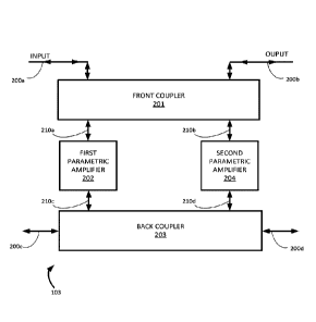
[049] FIG. 2 illustrates a low-noise directional amplifier 103 according to
some
embodiments. The directional amplifier 103 has at least two external ports
that may be used
to connect to external devices, such as qubit 101 ¨ a first port 200a acting
as an input port,
and a second port 200b acting as an output port. Additional external ports may
also be used.
For example, in the embodiment shown in FIG. 2, two additional "cold load"
ports, port 200c
and port 200d are part of the device. However, ports 200c and 2004 are not
used to send or
receive signals ¨ they are connected to "cold loads" in that the loads
connected to those ports
are kept at millikelvin temperatures. The directional amplifier 103 may also
include internal
ports for connecting a first component of the directional amplifier 103 to a
second component
of the directional amplifier. For example, port 210a connects a front coupler
201 to a first
parametric amplifier 202, port 210b connects the front coupler 201 to a second
parametric
amplifier 204. port 210c connects the first parametric amplifier 202 to a back
coupler 203,
and port 210d connects the second parametric amplifier to the back coupler
203. The
adjective "front" refers to the fact that the front coupler 201 provides the
two external ports
(an input port 200a and an output port 200b) that connect the directional
amplifier 103 to
external components. The adjective "back" refers to the fact that the back
coupler 203 does
not connect to any external components that send a signal to or receive a
signal from the
directional amplifier 103.
[050] The embodiment of directional amplifier 103 shown in FIG. 2 comprises
four main
components: a first coupler 201 (referred to as a front coupler), a second
coupler 203
(refened to as a back coupler), a parametric amplifier 202 and a second
parametric amplifier
204. In some embodiments, the front coupler 201 is a symmetric coupler that
acts like a
beamsplitter for microwave input signals. For example, front coupler 201
includes the input
port 200a that is configured to receive the signal to be amplified, and may
transmit or reflect
page 8
CA 02927326 2016-04-13
WO 2015/057839 PCT/US2014/060694
an input signal to the ports 210a and 210b, respectively. Similarly, while
output port 200b is
configured to output the amplified signal, a signal representing noise and/or
reflections from
external components subsequent to the directional amplifier 103 may be
received by the
directional amplifier 103 via output port 200b and may be transmitted or
reflected to ports
210b and 210a, respectively. Based on reciprocity, it is also possible that
any signal received
by ports 210a and 210b from other portions of the directional amplifier 103
can transmit or
reflect the signal out either input port 200a or output port 200b. Some
embodiments are
configured such that, for the entire system of the directional amplifier 103
receiving a signal
via input port 200a, the probability amplitude of a signal being output via
input port 200a is
substantially equal to zero. This reduction of the probability amplitude
reduces feedback to
the system being measured/amplified by the directional amplifier 103 (e.g.,
qubit 101).
[051] The couplers 201 and 203 may have any suitable transmission and
reflection
amplitudes. For example, for a signal incoming to port 200a of the front
coupler 201, the
"transmission amplitude" of the front coupler 201 represents the probability
amplitude that
the signal will leave via internal port 210a, and the "reflection amplitude"
of the front coupler
201 represents the probability amplitude that the signal will leave via
internal port 210b. In
some embodiments, the front coupler 201 and the back coupler 203 may be
symmetric
couplers, meaning the amplitude of the transmission and reflection amplitudes
are equal. For
example, the transmission amplitude for a signal incoming to input port 1 of
the front coupler
201 may be 1/sqrt(2) and the reflection amplitude for a signal incoming to
input port 1 of the
front coupler 201 may be i/sqrt(2), where i= sqrt(-1). The back coupler 203 is
may have
arbitrary transmission amplitude a and arbitrary reflection amplitude i0,
where a and 13 are
both real numbers. In some embodiments, the back coupler may also be a
symmetric coupler
such that a = = 1/sqrt(2). Symmetric couplers are sometimes referred to as 3dB
couplers.
However, embodiments are not limited to any particular transmission or
reflection amplitudes
for the front coupler 201 and the back coupler 203. The back coupler 203 may
be
implements in any suitable way. For example, the back coupler may be used to
introduce a
lossy channel between the first parametric amplifier 202 and the second
parametric amplifier
204, in which case a lossy microwave transmission connection may be used
instead of a
hybrid coupler.
[052] The parametric amplifiers 202 and 204 may be any suitable phase-
preserving
amplifier. For example, in some embodiments, a Josephson Parametric Converter
(JPC) may
be used. The JPC is a non-degenerate phase-preserving amplifier based on a
ring of
Josephson junctions, and is discussed in more detail in connection with FIG. 3
and FIG. 4
page 9
CA 02927326 2016-04-13
WO 2015/057839 PCT/US2014/060694
below. The two parametric amplifiers 202 and 204 utilize a coherent pump
signal to perform
the amplification via three-wave mixing. In some embodiments, the phase of the
pump for
each amplifier may be unequal, but held at a constant relationship with each
other. For
example, the difference between the two pump phases may be held constant,
represented by
the formula: A(p = (pi ¨ (p2 = C, where 6ap is the difference between the pump
phase (pi of
the first amplifier 202 and the pump phase of the second amplifier cp2 of the
second amplifier
204. In some embodiments, Acp = TER, which increases the forward gain of the
amplifier
103. hi some embodiments, the reflection coefficient for the overall device
may be tuned to
be substantially zero so that components, such as qubit 101, are not disturbed
by reflections
from directional amplifier 103. In other embodiments, the phase may be tuned
such that a
reverse gain through the directional amplifier 103 is negligible at the
expense of having a
non-zero reflection coefficient. Such an embodiment may be useful in
application where
reducing the reverse gain is important and where the corresponding non-zero
reflection
coefficient will not create problems for other components of the system.
[053] FIG. 3 illustrates an example JPC 202 according to some embodiments. The
central
element of JPC 202 is a Josephson ring modulator 402, which is discussed in
more detail in
connection with FIG. 4. Signals are input and output from the JPC 202 via
ports 301-303.
Because JPC 202 is a parametric amplifier for microwave frequencies, the
nomenclature of
optical parametric amplifiers that implement three-wave mixing is adopted.
Accordingly,
port 301 corresponds to the "signal mode," which may include, for example,
microwave
radiation with a small intensity, which will be amplified by the JPC 202; port
302
corresponds to the "idler mode," which may be an empty mode with no microwave
radiation
present (i.e., a vacuum state); and port 303 corresponds to the "pump mode,"
which may
include, for example, microwave radiation with a much larger intensity than
the intensity of
the microwave radiation in the signal mode. The microwave radiation in the
pump mode is
what provides the energy to amplify the radiation in the signal mode. In some
embodiments,
port 301 of FIG. 3 corresponds to port 200a of FIG. 2 and port 302 of FIG. 3
corresponds to
port 200b of FIG. 2. In this way, the idler modes of the two JPCs 202 and 204
are connected
via the back coupler 203.
[054] The JPC 202 includes two transmission line resonators that support one-
half wave at
the operational frequency, e.g., the length of the resonator is substantially
equal to the length
of one-half of the operational wavelength . Any suitable transmission line
resonator may be
used, such as, for example, stripline resonators. In some embodiments, JPC 202
performs
page 10
CA 02927326 2016-04-13
WO 2015/057839 PCT/US2014/060694
non-degenerate amplification, which means the wavelength of the idler mode is
different
from the wavelength of the signal mode. In non-degenerate embodiments, the JPC
202
supports two fundamental modes of different frequency ¨ a first frequency cos
associated with
a signal and a second frequency coi associated with an idler. The modes may be
determined
by the length of two half-wave microstrip resonators of the JPC. To apply
gain, the ring is
pumped with a coherent non-resonant pump P at the sum frequency cop = cos +
w1. In non-
degenerate embodiments, the first transmission line resonator comprises
portion 321 and
portion 322 and supports the shorter wavelength idler mode than the second
transmission line
resonator, which comprises portion 323 and portion 324 and supports the longer
wavelength
signal mode. The two transmission line resonators cross each other at a
voltage node, where
the Josephson Ring Modulator (JRM) is disposed.
[055] Each portion of the transmission line resonators is associated with a
respective
coupling capacitor: portion 321 of the first transmission line resonator is
associated with
coupling capacitor 331, portion 322 of the first transmission line resonator
is associated with
coupling capacitor 332, portion 323 of the second transmission line resonator
is associated
with coupling capacitor 333.and portion 324 of the first transmission line
resonator is
associated with coupling capacitor 334. Coupling capacitors 331 and 332,
associated with
the idler mode, are coupled to the port 302 associated with the idler mode and
coupling
capacitor 333 is coupled to the port 301 associated with the signal mode.
Coupling capacitor
334 is shorted to ground 343 or a 5052 cold load.
[056] In some embodiments, the idler mode and the pump mode are mixed at a 180
degree
hybrid coupler 305. The frequency of the pump radiation, which is equal to the
sum of the
frequency of the signal radiation and the frequency of the idler radiation, is
not resonant with
the JPC 202. While not illustrated in FIG. 3, in some embodiments, instead of
connecting
coupling capacitor 334 to ground, the port 301 associated with the signal mode
may be input
into a hybrid coupler along with a 5052 cold load, the two outputs of the
hybrid coupler being
connected to coupling capacitor 333 and coupling capacitor 334.
[057] The JPC 202 is based on a Josephson ring modulator 310 (JRM), which
provides the
nonlinearity that results in the three-wave mixing process that amplifies the
radiation in the
signal mode. The JRM 310 including at least four superconducting tunnel
junctions
(Josephson junctions), which is flux biased with a flux of P0/2, ,where 00 =
h/2 e is the
quantum flux The Josephson ring modulator 310 acts as a nonlinear medium and
mixes the
frequencies by converting pump photons into signal and idler photons. In
particular,
page 11
CA 02927326 2016-04-13
WO 2015/057839 PCT/US2014/060694
amplification of the signal is achieved via down-conversion of the pump P into
microwave
photons at the signal frequency cos. The signal mode is well isolated from the
pump and idler
modes, keeping the signal free from noise from the pump and idler photons. The
phase
acquired during the transmission gain process of the JPC is non-reciprocal and
depends on
the phase of the pump P.
[058] FIG. 4A illustrates a schematic of a first JRM 400 according to some
embodiments.
The JRM 400 includes for input/output ports (1-4) and four Josephson junctions
410-413 in a
Wheatstone bridge-like configuration. In some embodiments, the four Josephson
junctions
410-413 have substantially the same properties. FIG. 4B illustrates a
schematic of a second
JRM 401 according to some embodiments. The JRM 401 includes for input/output
ports (1-
4),four Josephson junctions 410-413 in a Wheatstone bridge-like configuration,
and four
shunting Josephson junctions 420-423. The shunting Josephson junctions 420-423
may be
larger than the four Josephson junctions 410-413. Including the shunting
Josephson junctions
410-413 may increase the tenability of the JRM 401 relative to the unshunted
JRM 400. In
bother JRM 400 and JRM 401, the Josephson junctions 410-413 are what introduce
the
nonlinearity into the JPC 202.
[059] Though a particular type of JPC based on microstrip resonators is
illustrated above,
some embodiments may use other types of JPCs. For example, compact resonator
JPCs,
based on resonators created from capacitors and resonators rather than a
microstrip of a
particular length, and capacitively and inductively shunted JPCs, where the
capacitive
elements of the JPC are parallel plate capacitors and the inductance is
governed primarily by
the inductance of the Josephson junctions. Moreover, the parametric amplifiers
202 and 204
are not limited to JPCs at all. Any suitable phase-preserving amplifier may be
used.
[060] Whereas FIG. 2 is a schematic illustrating the physical ports and
connections of
directional amplifier 103, FIG. 5 is a schematic representation of directional
amplifier 103
where each line represents a path that a wave may take through the system. For
example, the
input port 1 is associated with two lines: a first line representing a wave
flowing into the
directional amplifier 103 and a second line representing a wave flowing back
out from the
directional amplifier 103. The lines in FIG. 5 are marked with an arrows
representing the
direction of the wave flow associated with each line.
[061] FIG. 5 illustrates the same main components of the directional amplifier
103 as well
as the relevant variables associated with each component's effects on waves
that enter the
directional amplifier 103. For example, the front coupler 201 is labeled with
the reflection
amplitudes and transmission amplitudes associated with each line. Because
front coupler
page 12
CA 02927326 2016-04-13
WO 2015/057839 PCT/US2014/060694
201 is a symmetric (3dB) coupler, the transmission amplitude for microwaves
entering port 1
and exiting port l' and the transmission amplitude for microwaves entering
port l' and
exiting port 1 and the transmission amplitude for microwaves entering port 2
and exiting port
2' and the transmission amplitudes for microwaves entering port 2' and exiting
port 2 are all
equal to 1/sqrt(2). Whereas the reflection amplitude for microwaves entering
port 1 and
exiting port 2', the reflection amplitude for microwaves entering port 2' and
exiting port 1,
the reflection amplitude for microwaves entering port 2 and exiting port 1',
and the reflection
amplitude for microwaves entering port 1' and exiting port 2 are all equal to
i/sqrt(2), where
i=sqrt(-1).
[062] Similarly, the back coupler 203 is associated with its own set of
transmission
amplitudes, a, and reflection amplitudes, 113, where a and 13 are both real
numbers. The
transmission and reflection amplitudes of the back coupler 203 may be tuned to
desired
values as illustrated below.
[063] The first parametric amplifier 202 and the second parametric amplifier
204 are each
associated with a reflection gain amplitude and a transmission gain amplitude
at the resonant
frequency, which are is denoted as r and s, respectively. The reflection and
transmission gain
amplitudes satisfy the relation r2 ¨ s2 =1. The gain amplitudes are complex
numbers, the
absolute value squared of the gain amplitudes representing the actual gain a
signal will
experience when reflected by or transmitted through the parametric amplifiers.
Some
embodiments, such as the one shown in FIG. 5, use the same r and s for both
the first
parametric amplifier 202 and the second parametric amplifier 204, however,
embodiments
are not limited to having the same gain amplitudes. Other embodiments may use
different
gains for the two amplifiers. Any suitable value of r and s may be used. In
some
embodiments, the reflection gain amplitude r is limited to be within the range
1 < r < a-1.
A reflection gain amplitude within this range may result in a more stable
feedback loop
within the directional amplifier 103.
[064] The first parametric amplifier 202 and the second parametric amplifier
204 are also
each associated with a phase that is determined by the phase of the pump used
to drive the
amplifiers. The first parametric amplifier 202 has a first phase, (pi , and
the second
parametric amplifier 202 has a first phase. (1)7. The difference between the
first phase the
second phase may be set to any value. For example, in some embodiments, the
difference
between the first phase the second phase is equal to pi/2 radians (or 90
degrees), i.e., (pi - (1)2 =
It/2.
page 13
CA 02927326 2016-04-13
WO 2015/057839 PCT/US2014/060694
[065] There are four paths through the directional amplifier 103 illustrated
in FIG. 5 that
ultimately lead from input port 1 to output port 2, that will be illustrated
in connection with
FIG. 6A-D. Each figure shows the same directional amplifier 103 as illustrated
in FIG. 5, but
with arrows highlighting a particular path through the amplifier 103.
[066] In the first path, illustrated in FIG. 6A, a signal incoming to port 1
is transmitted with
transmission amplitude 1/sqrt(2) through the front coupler 201 to port 1'.
Upon reaching the
first parametric amplifier 202, the signal is reflected, with a gain amplitude
r, back to the
front coupler 201. At the front coupler 201, the signal is reflected with
reflection amplitude
i/sqrt(2) to the output port 2, where the signal exits the device 103.
[067] In the second path, illustrated in FIG. 6B, a signal incoming to port 1
is reflected with
reflection amplitude i/sqrt(2) in the front coupler 201 to port 2'. Upon
reaching the second
parametric amplifier 204, the signal is reflected with a gain amplitude r back
to the front
coupler 201. At the front coupler 201, the signal is transmitted with
transmission amplitude
1/sqrt(2) to the output port 2, where the signal exits the device 103.
[068] In the third path, illustrated in FIG. 6C, a signal incoming to port 1
is transmitted with
transmission amplitude 1/sqrt(2) through the front coupler 201 to port 1'.
Upon reaching the
first parametric amplifier 202, the signal is transmitted with a gain
amplitude s and a phase
(pi to the second parametric amplifier 204. At the second parametric amplifier
204, the
signal is transmitted with a gain amplitude of s and a phase of (p2 to the
front coupler. At the
front coupler 201, the signal is transmitted with transmission amplitude
1/sqrt(2) to the
output port 2, where the signal exits the device 103.
[069] In the fourth path, illustrated in FIG. 6D, a signal incoming to port 1
is reflected with
reflection amplitude i/sqrt(2) in the front coupler 201 to port 2'. Upon
reaching the second
parametric amplifier 204, the signal is transmitted with a gain amplitude s
and a phase (p2 to
the first parametric amplifier 202. At the first parametric amplifier 202, the
signal is
transmitted with a gain amplitude of s and a phase of (pi to the front
coupler. At the front
coupler 201, the signal is reflected with reflection amplitude 1/sqrt(2) to
the output port 2,
where the signal exits the device 103.
[070] These four paths add coherently such that the paths interfere with one
another,
resulting in the desired amplification of the received microwave signal. It is
possible to
express the effect of the directional amplifier 103 in terms of the various
parameters of the
components of the directional amplifier 103 using a "scattering matrix," which
maps how
signal input into any of the four ports of the device is transformed by the
directional amplifier
page 14
CA 02927326 2016-04-13
WO 2015/057839 PCT/US2014/060694
103 into an output signal that is output from the four ports. Thus, a
scattering matrix S is
defined as:
5, 5-
1 12 13 S14 \
1,
091 022 523 524
[Sr = (Equation 1)
S' 533
L 32 534
= 841. 842 S43 S44 I
where Sii represents the scattering amplitude for a signal input into port j
and output from port
i. In some embodiments, when all the components of the directional amplifier
103 are taken
into account, the scattering matrix simplifies into the form illustrated
below. In said
embodiments, the back coupler's transmission and reflection amplitudes are set
such that a =
13 = 1/sqrt(2) and the phase difference between the two parametric amplifiers
is set such that
= Tr/2. In this case, the scattering matrix of the directional amplifier 103
simplifies to
0 i.\/H / __
V 2 V 2
= G U = / __
[S]
V2'= G¨
v (Equation 2)
/c-1 = .11- ¨1 \./777 VT1 VT; ¨ /77
V 2 \I 2 9 2
G ¨1 = \I II ¨1 ¨ C
\ \I 2 '1 = 9
9 2
where the following parameter definitions are used:
y + h. = VG, (Equation 3)
(Equation 4)
g ¨ h. = -V H
+ 82 (Equation 5)
9= ________ _ s 2 '
and
(Equation 6)
= ______
1 82 '
[071] The above Equations 2-6 illustrate that, when the front coupler and back
coupler
amplitudes are fixed and the phase difference is fixed, the entire scattering
matrix of the
page 15
CA 02927326 2016-04-13
WO 2015/057839 PCT/US2014/060694
directional amplifier 103 may be written such that the only parameter is the
transmission gain
amplitude s of the two parametric amplifiers. Thus, it is possible to
determine how the
directional amplifier 103 behaves when the device is "off' by setting s = 0.
This may be
done by turning off the pump signal or otherwise preventing the pump signal
from entering
the parametric amplifiers 202 and 204. When the directional amplifier 103 is
off, the
scattering matrix reduces to:
/() 1 0 0 \
0 0 0
[S] = 0 () 0 = (Equation 7)
\ 0 0 0 ¨1 I
[072] The scattering matrix of Equation 7 indicates that when the directional
amplifier 103
is turned off, the transmission amplitude from the input port 1 to the output
port 2 is unity.
Accordingly, the device connected to port 1 from which the signal is obtained
(e.g., a
superconducting qubit 101), may be measured using alternative measurement
means without
disconnecting the directional amplifier 103 or using a switch to switch
between the
directional amplifier and the alternative measurement means.
[073] In the "high gain limit," where the parametric amplifiers are pumped
with as much
gain as physically possible, s = 1. Using Equations 5 and 6, the limit from
below of the
scattering matrix may be calculated to determine how the directional amplifier
acts in this
high gain limit as s approaches unity. In the high gain limit:
VG =cc
and
(Equation 8)
3 (Equation 9)
= ____________
2 T.
[074] Thus, the scattering matrix for the directional amplifier becomes:
page 16
CA 02927326 2016-04-13
WO 2015/057839 PCT/US2014/060694
0 4 4
G-1 ic;
Al 2
[S vG
r ________________________ -
)(i -1 1 (-17 r---7 (7'
-
i _____________________________________________________ (Equation 7)
\ 2 4
IG ________________________ -1 1
.
4 2
[075] Thus, in the high gain limit, the theoretical gain for a signal input
via port 1 of
directional amplifier 103 is infinite while the reverse gain of the device is
limited to I S1212 =
9/8, which is very near unity. Accordingly, in some embodiments, the
directional amplifier
103 has potentially unlimited forward gain while limiting the amount of
reverse gain through
the device. Also, input port 1 and output port 2 are perfectly matched such
that S11 = S22 =
0, indicating that there is no reflection signal even at the high gain limit.
[076] The above embodiments thus illustrate an embodiment of a non-reciprocal
directional
amplifier capable of quantum-limited operation with, in principle, no
limitation on the
forward gain and 9/8 limit on the reverse gain.
[077] In other embodiments, it may be desirable to reduce the reverse gain
(e.g., element S21
of the scattering matrix) through the directional amplifier 103. Accordingly,
the scattering
matrix may be tuned such that a reverse gain through the directional amplifier
103 is
negligible at the expense of having a non-zero reflection coefficient. Such an
embodiment
may be useful in application where reducing the reverse gain is important and
where the
corresponding non-zero reflection coefficient will not create problems for
other components
of the system.
[078] FIG. 7 illustrates a method 700 of amplifying a signal according to some
embodiments. At act 702, a microwave signal is received at an input port of a
directional
amplifier such as the directional amplifier according to some of the
embodiments illustrated
above. At act 704, the received microwave signal is split at a hybrid coupler
into two
portions. The signal may further be split into additional portions at a first
parametric
amplifier and/or a second parametric amplifier based on whether the respective
amplifier
reflects or transmits the received signal.
At act 706, at least a portion of the signal is amplified by both the first
parametric amplifier
and the second parametric amplifier. In some embodiments, the first parametric
amplifier is
pumped using a first microwave pump with a first phase and the second
parametric
page 17
CA 02927326 2016-04-13
WO 2015/057839 PCT/US2014/060694
amplifier is pumped using a second microwave pump with a second phase. In some
embodiments, the difference between the first phase and the second phase is
pi/2 radians.
[079] While embodiments of the low-noise directional amplifier are illustrated
above as
being used to measure a superconducting qubit, embodiments may be used in a
variety of
applications. For example, embodiments may be used to initialize and/or
perform quantum
gate operations on superconducting qubits.
[080] While embodiments of the low-noise directional amplifier may be used to
measure the
state of a superconducting qubit, embodiments may be used in a variety of
applications. For
example, embodiments may be used to initialize and/or perform quantum gate
operations on
superconducting qubits. Embodiments may also have applications outside of
quantum
information processing. For example, embodiments may be used in any situation
where
detection of low intensity microwave radiation is being performed, such as
microwave
telescopes used in astronomy or the detection of radar signals.
[081] Having thus described and illustrated several aspects of at least one
embodiment of a
low-noise directional amplifier it is to be appreciated that various
alterations. modifications,
and improvements will readily occur to those skilled in the art. Such
alterations,
modifications, and improvements are intended to be part of this disclosure,
and are intended
to be within the spirit and scope of the invention. While the present
teachings have been
illustrated in conjunction with various embodiments and examples, it is not
intended that the
present teachings be limited to such embodiments or examples. On the contrary,
the present
teachings encompass various alternatives, modifications, and equivalents, as
will be
appreciated by those of skill in the art. Those skilled in the art will
readily appreciate that all
parameters. dimensions, materials, and configurations described are provided
as non-limiting
examples and that the actual parameters, dimensions, materials, and/or
configurations will
depend upon the specific application or applications for which the inventive
teachings is/are
used. Those skilled in the art will also recognize, or be able to ascertain
using no more than
routine experimentation, many equivalents to the specific inventive
embodiments described.
It is, therefore, to be understood that the foregoing embodiments are
presented by way of
example only and that, within the scope of the invention, inventive
embodiments may be
practiced otherwise than as specifically described and claimed. Inventive
embodiments of
the present disclosure may be directed to each individual feature, system,
system upgrade,
and/or method described. In addition, any combination of two or more such
features,
systems, and/or methods, if such features, systems, system upgrade, and/or
methods are not
mutually inconsistent, is included within the inventive scope of the present
disclosure.
page 18
CA 02927326 2016-04-13
WO 2015/057839 PCT/US2014/060694
[082] Further, though some advantages of the described embodiments may be
indicated, it
should be appreciated that not every embodiment will include every described
advantage.
Some embodiments may not implement any features described as advantageous.
Accordingly, the foregoing description and drawings are by way of example
only.
[083] The indefinite articles "a" and "an," as used herein, unless clearly
indicated to the
contrary, should be understood to mean "at least one."
[084] The phrase "and/or," as used herein, should be understood to mean
"either or both" of
the elements so conjoined, i.e., elements that are conjunctively present in
some cases and
disjunctively present in other cases. Multiple elements listed with "and/or"
should be
construed in the same fashion, i.e., "one or more" of the elements so
conjoined. Other
elements may optionally be present other than the elements specifically
identified by the
"and/or" clause, whether related or unrelated to those elements specifically
identified. Thus,
as a non-limiting example, a reference to "A and/or B", when used in
conjunction with open-
ended language such as "comprising" can refer, in one embodiment, to A only
(optionally
including elements other than B); in another embodiment, to B only (optionally
including
elements other than A); in yet another embodiment, to both A and B (optionally
including
other elements); etc.
[085] As used herein, -or" should be understood to have the same meaning as -
and/or" as
defined above. For example, when separating items in a list. "or" or "and/or"
shall be
interpreted as being inclusive, i.e., the inclusion of at least one, but also
including more than
one, of a number or list of elements, and, optionally, additional unlisted
items. Only terms
clearly indicated to the contrary, such as "only one of' or "exactly one of,"
will refer to the
inclusion of exactly one element of a number or list of elements. In general,
the term "or" as
used shall only be interpreted as indicating exclusive alternatives (i.e. "one
or the other but
not both") when preceded by terms of exclusivity, such as "either," "one of,"
"only one of,"
or "exactly one of."
[086] As used herein, the phrase "at least one," in reference to a list of one
or more
elements, should be understood to mean at least one element selected from any
one or more
of the elements in the list of elements, but not necessarily including at
least one of each and
every element specifically listed within the list of elements and not
excluding any
combinations of elements in the list of elements. This definition also allows
that elements
may optionally be present other than the elements specifically identified
within the list of
elements to which the phrase "at least one" refers, whether related or
unrelated to those
elements specifically identified. Thus, as a non-limiting example, "at least
one of A and B"
page 19
CA 02927326 2016-04-13
WO 2015/057839 PCT/US2014/060694
(or, equivalently, "at least one of A or B," or, equivalently "at least one of
A and/or B") can
refer, in one embodiment, to at least one, optionally including more than one,
A. with no B
present (and optionally including elements other than B); in another
embodiment, to at least
one, optionally including more than one, B, with no A present (and optionally
including
elements other than A); in yet another embodiment, to at least one, optionally
including more
than one, A, and at least one, optionally including more than one, B (and
optionally including
other elements); etc.
[087] All transitional phrases such as "comprising," "including," "carrying,"
"having,"
"containing," "involving," "holding," "composed of," and the like are to be
understood to be
open-ended, i.e., to mean including but not limited to. Only the transitional
phrases
"consisting of' and "consisting essentially of" shall be closed or semi-closed
transitional
phrases, respectively.
What is claimed is:
page 20