Note: Descriptions are shown in the official language in which they were submitted.
CA 02928189 2016-04-28
275613
GATE DRIVE CIRCUIT TO REDUCE PARASITIC COUPLING
I. FIELD OF INVENTION
[0001] The present invention relates to a power electronic system that
employs a
transformer based gating system for voltage isolated active power devices.
11. BACKGROUND OF THE INVENTION
[0002] A number of different power conversion systems convert power from
one form
to another. For example, a multilevel power inverter is a power electronic
device structured
to produce alternating current (AC) waveforms from a direct current (DC) input
voltage.
These power conversion systems are used in a wide variety of applications,
such as variable
speed motor drives.
[0003] Isolation, and independent control within power conversion systems,
is
provided by gate drive circuitry. Gate drive circuits convert logic level
control signals into
appropriate voltages for switching one or more power devices within a power
semiconductor group. In most cases, these circuits provide voltage isolation
to prevent
exposure of the logic signals to potentially dangerous high voltages on the
power circuit.
[0004] Many conventional techniques provide isolation and control
functionality via
gate drive circuits. For example, one technique transfers a voltage directly
across a barrier,
via a transformer, while maintaining galvanic isolation. When using a
transformer, a
voltage common to terminals of the secondary is produced when a voltage step
occurs
within the power semiconductor group. This common voltage causes parasitic
currents to
flow through the control circuit, which can cause failure or unintended
operation. Another
technique uses fiber optic transmission for creating the digital on-off
signal, while
transferring power separately with an isolated power source. These
conventional
techniques, however, are costly and lack precision synchronization for
controlling series
connected power semiconductor devices (e.g., switches).
1
CA 02928189 2016-04-28
275613
III. SUMMARY OF EMBODIMENTS OF THE INVENTION
[0005] Given the aforementioned problem, a need exists for systems and
methods that
provide precise synchronization for controlling series connected power devices
for circuits
to perform in high voltage environments with a significant amount of rate of
change in
voltage with respect to time.
[0006] The present invention includes a drive circuit, for driving an
electrical system.
The drive circuit includes a first transformer unit in connection with a pulse
amplifier
module and a second transformer unit in connection with a plurality of power
semiconductor groups, each group containing one or more switching devices. The
first and
second transformers provide voltage isolation and reduce parasitic coupling
between the
control module and the pulse receiver module. With each additional transformer
added in
series between the first primary winding and last secondary winding,
additional capacitance
is added to the electrical system. Therefore, the collective capacitance
between the first
primary and the last secondary windings is decreased.
[0007] The first transformer unit includes at least one primary transformer
configured
to receive a current pulse at a primary winding from a current pulse
generation module
controlled by a control module. Additionally, the current pulse is reflected
to a secondary
winding.
[0008] The second transformer unit includes a plurality of secondary
transformers
where each secondary transformer is configured to receive the current pulse at
a primary
winding. Additionally, the current pulse is reflected to a secondary winding
coupled to a
pulse receiver module.
[0009] Further features and advantages of the invention, as well as the
structure and
operation of various embodiments of the invention, are described in detail
below with
reference to the accompanying drawings. It is noted that the invention is not
limited to the
specific embodiments described herein. Such embodiments are presented herein
for
2
CA 02928189 2016-04-28
275613
illustrative purposes only. Additional embodiments will be apparent to persons
skilled in
the relevant art(s) based on the teachings contained herein.
IV. BRIEF DESCRIPTION OF THE DRAWINGS
[0010] The accompanying drawings, which are incorporated herein and form
part of
the specification, illustrate the present invention and, together with the
description, further
serve to explain the principles of the invention and to enable a person
skilled in the relevant
art(s) to make and use the invention.
[0011] FIG. 1 is a schematic diagram of an exemplary embodiment of an
electronic
system in accordance with an embodiment of the present invention.
[0012] FIG. 2 is a schematic diagram illustration of logical level signals
determining
four types of current pulses in the gate drive circuit of the electronic
system of FIG. 1.
[0013] FIG. 3 is a schematic diagram of illustration of an electronic
system in
accordance with a second embodiment of the present invention.
[0014] FIG. 4 is a schematic diagram of illustration of an electronic
system in
accordance with a third embodiment.
V. DETAILED DESCRIPTION OF THE PREFERRED EMBODIMENTS
[0015] While the present invention is described herein with illustrative
embodiments for
particular applications, it should be understood that the invention is not
limited thereto.
Those skilled in the art with access to the teachings provided herein will
recognize
additional modifications, applications, and embodiments within the scope
thereof and
additional fields in which the invention would be of significant utility.
[0016] Unless defined otherwise, technical and scientific terms used herein
have the
same meaning as is commonly understood by one of ordinary skill in the art to
which this
disclosure belongs. The terms "first," "second," and the like, as used herein
do not denote
any order, quantity, or importance, but rather are used to distinguish one
element from
3
CA 02928189 2016-04-28
275613
another. Also, the terms "a" and "an" do not denote a limitation of quantity,
but rather
denote the presence of at least one of the referenced items. The term "or" is
meant to be
inclusive and mean either, any, several, or all of the listed items.
[0017] The use of "including," "comprising," or "having" and variations
thereof herein
are meant to encompass the items listed thereafter and equivalents thereof as
well as
additional items. The terms "connected" and "coupled" are not restricted to
physical or
mechanical connections or couplings, and can include electrical connections or
couplings,
whether direct or indirect. The terms "circuit," "circuitry," and "controller"
may include
either a single component or a plurality of components, which are either
active and/or
passive components and may be optionally connected or otherwise coupled
together to
provide the described function.
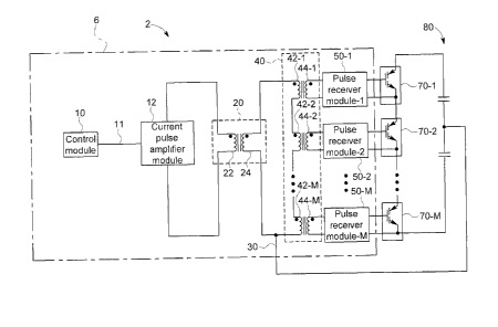
[0018] FIG. 1 is an illustration of an exemplary electronic system 2
including a drive
circuit 6 connected to a plurality of semiconductor groups 70. The drive
circuit 6 includes
a control module 10, a current pulse amplifier module 12, a first transformer
unit 20, and a
second transformer unit 40.
[0019] Control module 10 of gate drive circuit 6 includes one or more
devices capable
of generating logic level control signals based on particular programming.
According to an
embodiment, control module 10 is programmed to generate a number of logic
level signals
for shaping a current pulse to be output to the current pulse amplifier module
12. As
described below, the current pulse is used to produce the voltage signals
driving power
devices of each semiconductor group 70.
[0020] The power devices are semiconductors used as a switch or a rectifier
capable of
being selectively changed between a non-conducting (off) state and a
conducting (on) state
as commanded by a control input signal, and shall include, for example
thyristors, bipolar
junction transistors (BJTs), insulated gate bipolar transistors (IGBTs), or a
metal oxide
semiconductor field-effect transistors (MOSFETs), among others. The power
devices can
be classified into two categories with respect to drive requirements, namely
non-gate oxide-
4
CA 02928189 2016-04-28
275613
isolated active power semiconductor devices and gate oxide-isolated active
power
semiconductor devices.
[0021] The control module 10 communicates with the current pulse amplifier
module
12 by way of one or more logic signals 11. The current pulse amplifier module
12 outputs
current pulses based on the logic signals 11, output from the control module
10.
[0022] As illustrated in FIG. 2, the logic signals 11 may include one of
any number of
current pluses, that transitions through three logical states (e.g., High,
Low, Neutral). The
current pulse, for example, can include (i) a Turn Off Pulse that transitions
each
semiconductor within each semiconductor group 70 from a conducting (on) state
to a non-
conducting (off) state. The current pulse can also include a (ii) a Turn On
Pulse, that
transitions each semiconductor of each semiconductor group 70 from a non-
conducting
state to a conducting state, and (iii) a Refresh Off Pulse, that maintains
each semiconductor
of each semiconductor group 70 in a non-conducting state when the power
devices are
already in an Off state. Additionally, (iv) a Refresh On Pulse maintains each
semiconductor
of each semiconductor group 70 in a conducting state when the power devices
are already
in an On state.
[0023] As depicted in FIG. 2, the control module 10 outputs two types (turn
off, and
turn on pulses) of logic signals 11 to the current pulse amplifier module 12,
each
representing a type of current pulse. For example, a logic signal A
transitions through three
logical states (e.g., High, Low, Neutral) and another logic signal 11 (Logic
Signal B) only
transitions through two logical states (e.g., High, Low).
[0024] In the electronic system 2 of FIG. 2, logic signal B produces a zero
volt state
across the first transformer unit 20 when logic signal A is in the neutral
state. This
arrangement ensures the second transformer unit 40 does not pull charge from
gates of
switches within the semiconductor groups 70 after the current pulse has been
released.
[0025] The current pulse produced by logic signal A, and provided to the
current pulse
amplifier module 12, is provided to windings of the transformer unit 20,
specifically to
CA 02928189 2016-04-28
275613
primary windings 22. In response, a current pulse is reflected on secondary
windings 24 of
the first transformer unit 20. In other words, provision of the current pulse
generated by
logic signal A to the primary windings 22 will result in M substantially
identical reflected
current pulses scaled by the secondary windings 24 to a turns ratio at the
secondary
windings 24.
[0026] One advantage of using the first transformer unit 20 in this manner
is that it
provides the M reflected current pulses at the secondary windings 24 in a
synchronized
manner while simultaneously providing voltage isolation between control module
10 and
logic signal to the current pulse amplifier module 12 and the higher
(potentially dangerous)
voltage of active power semiconductor groups 70.
[0027] The first transformer unit 20 includes primary windings 22 coupled
to
secondary windings 24. In some embodiments, the primary windings 22 are
identical to
one another and the secondary windings 24 are identical to one another (e.g.,
the same
magnetic core, turns ratio, and leakage inductance is employed). In other
embodiments,
however, the primary windings 22 and the secondary windings 24 may differ from
one
another.
[0028] In high common mode environments, parasitic capacitive coupling
between the
semiconductor groups 70 and the drive circuit 6 can negatively affect the
performance of
the system 2, resulting in failure or unintended operation of components of
the drive circuit
6. Specifically, a high rate of change in voltage with respect to time (dv/dt)
of the power
semiconductors causes a large voltage step to develop on primary windings
(e.g., primary
windings 42 of the second transformer unit 40), with respect to a control
voltage reference
node. This voltage step results in a flow of a common mode current from the
power devices
within the semiconductor groups 70 towards the current pulse amplifier module
12 and the
control module 10. This common mode current can interrupt typical switching of
low-
voltage power devices within the pulse amplifier module 12, for example, and
result in
unintended operation of those low-voltage power devices. Additionally,
unintended
operation may lead to failure of the power devices within the semiconductor
groups 70.
6
CA 02928189 2016-04-28
275613
[0029] Additionally, common mode voltage isolation is not present within
the system
2. Common mode voltage can cause common mode current flow through low voltage
electronics and ground loops in measurement systems that have multiple
grounding
locations. Common mode voltage that exceeds the maximum an overvoltage rating
of the
switches within the semiconductor groups 70 may damage components of the drive
circuit
6.
[0030] Presence of the first transformer unit 20 reduces the dv/dt stresses
of the control
module 10 that occur when the power devices within the semiconductor groups 70
switch
by increasing common mode impedance within the system 2. For example, the
first
transformer unit 20 lowers capacitance between the control module 10 and the
power
devices within the semiconductor groups 70. Including a transformer winding in
series
increases capacitance of the drive circuit 6 by virtue of series capacitance
and thus
decreases the overall capacitive coupling between the first primary winding
and the last
secondary winding.
[0031] In other embodiments, as illustrated in FIGs. 3 and 4, the first
transformer unit
20 can include up to N primary windings 22 (labeled 1 through N) coupled to N
secondary
windings 24 (labeled 1 through N). Each of the M primary windings 22 is
identical to other
primary windings 22. Similarly, each of the M secondary windings 24 is
identical to other
secondary windings 24 (i.e., the same magnetic core, turns ratio, and leakage
inductance is
employed).
[0032] Each primary winding 22 (1 through N) of second transformer unit 40
may
wired in parallel to allocate current. In parallel configurations, the output
of the logic signal
11 to the current pulse amplifier module 12 is provided to the primary winding
22 of a first
transformer 20-.1 within the first transformer unit 20.
[0033] Alternatively, the primary windings 22 (1 through N) can be
connected to one
another in series so that all transformers within the first transformer unit
20 will have the
same current. In series configurations, the output of logic signal 11 to the
current pulse
amplifier module 12 is provided to each primary winding 22 of first
transformer unit 20
7
CA 02928189 2016-04-28
275613
such that each primary winding 22 will receive the same signal (i.e., the same
current pulse)
output from the current pulse amplifier module 12.
[0034] In some embodiments, a loop 30 connects the first transformer unit
20 and the
second transformer unit 40. Specifically, the loop 30 connects the secondary
windings 24
of the first transformer unit 20 to a potential within the system 2. By
connecting the first
transformer unit 20 to a potential within the system 2, capacitive coupling is
decreased.
[0035] In other embodiments, the loop 30 is connected to a potential
located at a
midpoint of the system 2. An example configuration, as illustrated in FIG. 1,
depicts the
loop 30 in connection connects to a DC link 80 of the system 2.
[0036] Specifically, the loop 30 provides additional pathways of current
flow back to
the source of the common mode voltage and allows the common mode current to be
directed away from gating electronics (e.g., the gate circuit 2). The loop 30
provides a low
impedance path from the semiconductor group 70 back to the source of the
reference node
of the voltage step change. The connection of the drive circuit 6 to a voltage
potential
results in a higher parasitic impedance from the current pulse amplifier
module 12 back to
the loop 30 rather than through the same connection at the primary windings
42, resulting
in current flow along a path of least impedance that circumvents electronics
within the
control module 10.
[0037] Where multiple transformers exist in the first transformer unit 20,
as illustrated
in FIGs. 3 and 4, each of the first transformer units 20-1 through 20-N have
an associated
loop 30 (labeled 1 through N). Each of the loops 30-1 through 30-N are
connected to a
voltage potential of the system 2.
[0038] In some multiple transformer embodiments, each loop 30 may be
connected to
the same potential within the system 2. For example, the loops 30-1 through 30-
N may be
connected to the midpoint of a DC link 80. In another example, illustrated in
FIG. 3, the
first loop 30-1, the second loop 30-2, and the Nth loop 30-N may each be in
connection
with one of the semiconductor groups 70 (e.g., 70-2 as illustrated).
8
CA 02928189 2016-04-28
275613
[0039] In some multiple transformer embodiments, one or more loops 30 can
be
connected to different potentials within the system 2. For example, as
illustrated in FIG.
4, the loops 30-1 and 30-N are connected to the midpoint of the DC capacitor
link 80.
However, the loop 30-2 is connected to the second semiconductor group 70-2.
[0040] The drive circuit 6 also includes the second transformer unit 40.
The second
transformer unit 40 receives pulses from the current pulse amplifier module 12
by way of
the first transformer unit 20.
[0041] The second transformer unit 40 comprises M primary windings 42
(labeled 1
through M) coupled to M secondary windings 44 (labeled 1 through M, in the
manner
described above.
[0042] The primary windings 42-1 through 42-M of the second transformer
unit 40 are
connected in series so that all transformers within the second transformer
unit 40 will have
the same signal (current pulse). That is, current pulses received by the
primary windings
42 of the second transformer unit 40 will result in M substantially identical
reflected current
pulses scaled by the secondary to primary turns ratio at the secondary
windings 44.
[0043] A benefit of using the second transformer unit 40 in this manner is
that it
provides the M reflected current pulses at the secondary windings 44 in a
synchronized
manner. This occurs while simultaneously adding capacitance in series between
the control
module 10 and logic signal to the current pulse amplifier module 12 and the
higher
(potentially dangerous) voltage of semiconductor groups 70. That is, the first
transformer
unit 20 and the second transformer unit 40 collectively increase the common
mode
impedance between the control module 10 and each of the pulse receiver modules
50-1
through 50-M.
[0044] Each of the secondary windings 44-1 through 44-M of the second
transform
unit 40 connects to M pulse receiver modules 50 (labeled 1 through M). Each
pulse
receiver module 50 is coupled to gate(s) of the switches of an associated one
of the
semiconductor groups 70.
9
CA 02928189 2016-04-28
275613
[0045] Each pulse receiver module 50 transfers and latches the received
current pulse
appropriate for driving the switches of the associated semiconductor group 70.
More
specifically, each pulse receiver module 50 performs two main functions on the
received
current pulses to establish a voltage (e.g., gate-to-emitter voltage) to drive
switches of the
semiconductor groups 70 either conducting (on state) or not conducting (off
state).
[0046] First, the pulse receiver module 50 sets up and clamps to an on
state gate-to-
emitter voltage for a positive current pulse. Likewise, the pulse receiver
module 50 sets up
and clamps to an off state gate-to-emitter voltage for a negative current
pulse.
[0047] Second, the pulse receiver module 50 remains at the on state or off
state gate-
to-emitter voltage after the current pulse has ended so that the switches
within an active
power semiconductor group 70 can remain in either the on state or off state,
respectively.
This prevents a flux reset action of the second transformer unit 40 from
inadvertently
disturbing the proper on state and off state gate-to-emitter voltages.
[0048] Components within the electronic system 2 may be hardened to
electromagnetic
interference (EMI) to be more robust against the presence of electromagnetic
waves in the
air. Such EMI hardened components may prevent detected signals from
propagating to the
connected circuitry on the drive circuit 6.
[0049] It is to be appreciated that the Detailed Description section, and
not the
Summary and Abstract sections, is intended to be used to interpret the claims.
The
Summary and Abstract sections may set forth one or more but not all exemplary
embodiments of the present invention as contemplated by the inventor(s), and
thus, are not
intended to limit the present invention and the appended claims in any way.