Note: Descriptions are shown in the official language in which they were submitted.
CA 2928598
SUBSTRATES COMPRISING NANO-PATTERNING SURFACES AND METHODS OF
PREPARING THEREOF
[0001] <deleted>
FIELD
[0002] In general, the present application relates to the fields of
nano-patterning
process and substrates comprising nano-patterning surfaces. More specifically,
the present
application relates to substrates comprising at least two and in some
embodiments at least three
layers, including a polymer layer comprising nano-scale and micro-scale
patterns. Methods of
preparing these substrates by using a resist-free, room temperatures UV curing
and embossing
processes are also disclosed.
BACKGROUND
[0003] Nano-imprinting technology enables the economic and effective
production of
nanostructures. Standard nano-embossing lithography relies on direct
mechanical deformation of
the resist materials by a stamp having nanostructures, followed by an etching
process to transfer the
nanostructures from the stamp to the substrate.
SUMMARY
[0004] The current application utilizes a UV sensitive polymer to form
a polymer layer
with a plurality of micro-scale or nano-scale patterns. The UV release process
prevents the stiction
of the polymer to the template and prevents any deformation of the patterns
during separation,
hence giving robust pattern transfer even at nano-scale. The process of the
present application is
complementary to the thermal embossing process and does not require heating
the master template
and thereby avoids issues related to thermal stresses in materials and thermal
gradients across the
template.
[0005] The processes of the present application can be applied to
technologies where
low-cost micro and nano-patterning may be necessary. Applications include nano-
manufacturing,
medical diagnostics and global health, flexible display technology,
nanofluidics, as well as
emerging markets including the construction and automotive industries where
low-
- 1 -
Date Recue/Date Received 2022-02-16
CA 02928598 2016-04-22
WO 2015/095291 PCT/US2014/070777
cost methods to generate nano-patterned, super hydrophobic surfaces (dewetting
windows,
windscreens etc.) are gaining traction. The processes of the present
application can also be
applied to generate low-cost patterned consumables, for example, patterned
plastic flowcells and
low-cost microfluidic devices for use in sequencing devices.
[0006] With the spiraling cost of healthcare and the lack of medical
infrastructure in
developing nations, there is an increasing demand for point-of-care (POC)
diagnostics and low
cost Lab-on-a-Chip (LOC) technologies. Broadened applicability of these
technologies can
follow if they are made more cheap, robust, portable, disposable and most
importantly, provide
rapid time to result. To enable such advances. low cost patterning and
microfluidic technologies
are desired. Paper-based microfluidics have emerged as one potential
candidate, but are difficult
to fabricate using conventional lithography based approaches, are difficult to
multiplex for the
detection of multiple analytes, and readily wick solutions thereby requiring
pre-concentration of
the target analytes in many embodiments. The processes of the present
application provide a
highly cost-effective alternative to fabricating microfluidic based total
analysis platforms for
global health applications.
10007] Some embodiments disclosed herein include a substrate comprising
a
functionalizable layer comprising one or more functional groups; a polymer
layer comprising a
plurality of micro-scale or nano-scale patterns, or combinations thereof: and
a backing layer.
[0008] In some embodiments, the functionalizable layer is disposed
between the
backing layer and the polymer layer. In some embodiments, the polymer layer is
disposed
between the backing layer and the functionalizable layer. In some embodiments,
the substrate
can further comprise a sealing layer to substantially seal the polymer layer
and the
functionalizable layer between the backing layer and the sealing layer. In
some such
embodiments, the sealing layer is optically transparent.
[0009] In some embodiments, at least one of the micro-scale or nano-
scale patterns is
capable of admitting a sample fluid. In some embodiments, the substrate can
further comprise a
fluid reservoir, for example, a sample reservoir.
[0010] In any of the disclosed embodiments, the functionalizable layer
can comprise
a reactive silane layer, a functionalizable hydrogel or a functionalizable
polymer. In some such
embodiments, the functionalizable layer can comprise one or more functional
groups. In some
such embodiments, the functional group can be selected from the group
consisting of optionally
substituted alkene, azide, optionally substituted amine, carboxylic acid,
optionally substituted
hydrazone, halogen, hydroxy, optionally substituted tetrazole, optionally
substituted tetrazine,
thiol, and combinations thereof.
-2-
CA 02928598 2016-04-22
WO 2015/095291 PCT/US2014/070777
[0011] In any of the disclosed embodiments, the functional groups of the
functionalizable layer can be attached to biomolecules. In some embodiments,
the biomolecules
arc selected from amino acids, nucleosides, nucleotides, peptides,
oligonucleotides,
polynucleotides, nucleic acids, proteins, or combinations thereof In some such
embodiments,
the biomolecules are polynucleotides or nucleic acids.
[0012] In any of the disclosed embodiments, the polymer layer comprises
at least one
photocurable polymer. In some embodiments, the photocurable polymer comprises
a urethane.
acrylate, silicone, epoxy, polyacrylic acid, polyacrylates, epoxysilicone,
epoxy resins.
polydimethylsiloxane (PDMS), silsesquioxane, acyloxysilanes, maleate
polyesters, vinyl ethers,
monomers with vinyl or ethynyl groups, or copolymers and combinations thereof.
[0013] Some embodiments disclosed herein include a process for preparing
a
substrate, comprising: providing a substrate comprising a functionalizable
layer comprising one
or more functional groups disposed between a backing layer and a layer of
photocurable
polymer; contacting a surface of the layer of photocurable polymer with a
template having a
plurality of micro-scale or nano-scale patterns including micro-scale or nano-
scale wells, posts,
or combinations thereof; applying pressure to the template or substrate to
transfer the micro-
scale or nano-scale patterns to at least the layer of photocurable polymer,
where the contacting
and applying are performed at room temperature; irradiating the photocurable
polymer with UV
light to cure the photocurable polymer; and separating the template from
substrate; where at least
a portion of the polymer layer is perforated to expose the underlying
functionalizable layer. In
some embodiments, at least a portion of polymer layer and functionalizable
layer are perforated
to expose the underlying backing layer.
[0014] Some embodiments disclosed herein include a process of preparing
a
substrate, comprising: providing a template comprising a plurality of micro-
scale or nano-scale
patterns including micro-scale or nano-scale wells, channels or combinations
thereof on a
surface of the template; depositing a functional layer comprising one or more
functional groups
on the surface of the template such that at least a portion of the micro-scale
or nano-scale wells,
channels or combinations thereof contain the functional layer: removing excess
functionalizable
layer from the surface of the template such that the functionalizable layer is
present on only a
portion of the template surface; providing a substrate comprising a backing
layer having a
photocurable polymer layer disposed on the backing layer; contacting a surface
of the
photocurable polymer layer with the surface of the template having the
plurality of micro-scale
or nano-scale patterns and functionalizable layer thereon; applying pressure
to the template or
substrate to transfer the micro-scale or nano-scale patterns to at least the
layer of photocurable
-3-
CA 2928598
polymer, where the contacting and applying are performed at room temperature;
irradiating the
photocurable polymer with UV light to cure the photocurable polymer; and
separating the template
from the substrate; where at least a portion of the functionalizable layer is
transferred to the
polymer layer. In some embodiments, at least a portion of polymer layer is
perforated to expose the
backing layer. In some embodiments, the substrate further comprises a backing
layer having a
photocurable polymer layer disposed on the backing layer is a roll of flexible
dicing tape.
[0015]
In any of the disclosed process embodiments, the process can further comprises
applying a sealing layer to the substrate after removing the template to
substantially seal the
polymer layer and the functionalizable layer between the backing layer and the
sealing layer. In
some embodiments, the sealing layer further comprises a second substrate
prepared by the process
of any of the disclosed embodiments, where the functionalizable layers and
photocurable polymer
layers of the substrates are disposed between the backing layers of the
substrates. In some
embodiments, the sealing layer is optically transparent. In some process
embodiments, the process
can be a roll to roll process.
[0015A] The invention disclosed and claimed herein pertains to a patterned
substrate
comprising: a functionalizable layer comprising one or more functional groups;
a UV-cured
polymer layer comprising a plurality of micro-scale or nano-scale patterns, or
combinations thereof;
and a backing layer; wherein the functionalizable layer comprises a reactive
silane layer, and a
functionalizable hydrogel or polymer, said functionalizable hydrogel or
polymer comprising the
one or more functional groups, wherein the one or more functional groups are
capable of attaching
to biomolecules, and wherein the UV-cured polymer layer comprises at least one
photocurable
polymer and is free of photoresist.
[0015B] Aspects of the disclosure relate to a process of preparing a patterned
substrate,
comprising: providing a substrate comprising a functionalizable layer
comprising one or more
functional groups disposed between a backing layer and a layer of photocurable
polymer;
contacting a surface of the layer of photocurable polymer with a template
having a plurality of
micro-scale or nano-scale patterns including micro-scale or nano-scale wells,
posts, or
combinations thereof, wherein the photocurable polymer layer is free of
photoresist; applying
pressure to the template or substrate to transfer said micro-scale or nano-
scale patterns to at least
the layer of photocurable polymer, wherein the contacting and applying are
performed at room
temperature; irradiating the photocurable polymer with UV light to cure the
photocurable polymer
to form a UV-cured polymer layer of the patterned substrate; and separating
the template
- 4 -
Date Re9ue/Date Received 2021-07-21
CA 2928598
from the patterned substrate; wherein at least a portion of the UV-cured
polymer layer is perforated
to expose the underlying functionalizable layer; and wherein the
functionalizable layer comprises a
functionalizable hydrogel or polymer, said functionalizable hydrogel or
polymer comprising said
one or more functional groups, and wherein said one or more functional groups
are capable of
attaching to biomolecules.
[0015C] Aspects of the disclosure relate to a process of preparing a patterned
substrate,
comprising: providing a template comprising a plurality of micro-scale or nano-
scale patterns
including micro-scale or nano-scale wells, channels, or combinations thereof
on a surface of the
template; depositing a functional layer comprising one or more functional
groups on the surface of
the template such that at least a portion of said micro-scale or nano-scale
wells, channels, or
combinations thereof contain said functional layer; removing excess
functionalizable layer from the
surface of the template such that the functionalizable layer is present on
only a portion of the
template surface; providing a substrate comprising a backing layer having a
photocurable polymer
layer disposed on the backing layer, wherein the photocurable polymer layer is
free of photoresist;
contacting a surface of the photocurable polymer layer with the surface of the
template having the
plurality of micro-scale or nano-scale patterns and functionalizable layer
thereon; applying pressure
to the template or substrate to transfer said micro-scale or nano-scale
patterns to at least the layer of
photocurable polymer, wherein the contacting and applying are performed at
room temperature;
irradiating the photocurable polymer with UV light to cure the photocurable
polymer to form a UV-
cured polymer layer of the patterned substrate; and separating the template
from the patterned
substrate; wherein at least a portion of the functionalizable layer is
transferred to the UV-cured
polymer layer; and wherein the functionalizable layer comprises a
functionalizable hydrogel or
polymer, said functionalizable hydrogel or polymer comprising said one or more
functional groups,
and wherein said one or more functional groups are capable of attaching to
biomolecules.
[0015D] Aspects of the disclosure relate to a roll-to-roll process of
preparing a patterned
substrate, comprising: contacting a template comprising a plurality of micro-
scale or nano-scale
patterns with a surface of a substrate comprising a photocurable polymer layer
disposed thereon;
applying pressure to the template or the substrate to transfer the micro-scale
or nano-scale patterns
to the photocurable polymer layer, wherein the contacting and applying are
performed at room
temperature; irradiating the photocurable polymer with UV light to cure the
- 4a -
Date Re9ue/Date Received 2021-07-21
CA 2928598
photocurable polymer to form a patterned UV-cured polymer layer; and
separating the template
from the substrate.
BRIEF DESCRIPTION OF THE DRAWINGS
[0016] FIGs. 1A - 1C are cross-section views of several embodiments of
a substrate
where a functionalizable layer is disposed between a polymer layer and a
backing layer.
[0017] FIGs. 2A - 2C are cross-section views of several embodiments of
a substrate
where a functionalizable layer is disposed between a polymer layer and a
backing layer.
100181 FIG. 2D is a top view of a substrate where a functionalizable
layer is disposed
between a polymer layer and a backing layer.
[0019] FIG. 2E is a cross-section view of a substrate where a
functionalizable layer
and a polymer layer are disposed between a backing layer and a sealing layer.
[0020] FIGs. 3A - 3C are cross-section views of several embodiments of
a substrate
wherein a polymer layer is disposed between a functionalizable layer and a
backing layer.
[0021] FIGs. 4A and 4B are cross-section views of several embodiments
of a substrate
where a functionalizable layer is disposed between a polymer layer and a
backing layer.
[0022] FIG. 4C is a cross-section view of a substrate where a
functionalizable layer
and a polymer layer are disposed between a backing layer and a sealing layer.
[0023] FIGs. 5A and 5B are cross-section views of several embodiments
of a substrate
in the shape of a cylinder.
- 4b -
CA 2928598 2019-12-16
CA 02928598 2016-04-22
WO 2015/095291 PCT/US2014/070777
[0024] FIGs. 6A and 6B are cross-section views of several embodiments of
a
substrate in the shape of a cylinder.
[0025] FIGs. 7A and 7B are cross-section views of several embodiments of
two
substrates stacking on top of another via contact or within close proximity of
their distal surfaces
(i.e. surfaces that are distal to their respective base layers).
[0026] FIGs. 8A - 8D are cross-section views describing an embodiment of
a process
for preparing a substrate where a functionalizable layer is disposed between a
polymer layer and
a backing layer using a template comprising a plurality of micro-scale or nano-
scale patterns.
[0027] FIGs. 9A - 9E are cross-section views describing an embodiment of
a process
for preparing a substrate where a polymer layer is disposed between a
functionalizable layer and
a backing layer using a template comprising a plurality of micro-scale or nano-
scale patterns.
[0028] FIG. 10A is a top view of an 8 inch mater template wafer
containing 12 Hi-
seq sized patterned flowcells.
[0029] FIG. 10B is a top view dark field microscope image of the cut out
Flowcell 7
from FIG. 10A.
[0030] FIGs. 10C - 1OF are top view SEM images of the nano-scale
patterns formed
on a polymer sheet at 1240X, 20kX, 40kX and 80kX magnification respectively.
[0031] FIGs. 11A and 11B are top view SEM images of nano-scale patterns
at 1307x
and 5000x magnification respectively.
[0032] FIG. 12A is a top view optical image of serpentine microfluidic
channels and
junctions.
[0033] FIG. I2B is a top view of an optical image of a microfluidic
filter.
[0034] FIG. 12C is a top view of an optical image of a fluid flow
through a
serpentine microfluidic channels as a function of time.
[0035] FIG. 12D is a top view of an optical image of a fluid flow into a
T-junction.
DETAILED DESCRIPTION OF THE PREFERRED EMBODIMENTS
[0036] The following detailed description is directed to certain
specific embodiments
of the present application. In this description, reference is made to the
drawings wherein like
parts or steps may be designated with like numerals throughout for clarity.
Reference in this
specification to "one embodiment," "an embodiment,- or "in some embodiments"
means that a
particular feature, structure, or characteristic described in connection with
the embodiment can
be included in at least one embodiment of the invention. The appearances of
the phrases "one
embodiment," "an embodiment," or "in some embodiments" in various places in
the
-5-
CA 2928598
specification are not necessarily all referring to the same embodiment, nor
are separate or
alternative embodiments mutually exclusive of other embodiments. Moreover,
various features are
described which may be exhibited by some embodiments and not by others.
Similarly, various
requirements are described which may be requirements for some embodiments but
not other
embodiments.
[0037] The section headings used herein are for organizational
purposes only and are
not to be construed as limiting the subject matter described.
Definitions
[0038] Unless defined otherwise, all technical and scientific terms
used herein have the
same meaning as is commonly understood by one of ordinary skill in the art. As
used in the
specification and the appended claims, the singular forms "a," "an" and "the"
include plural
referents unless the context clearly dictates otherwise. The use of "or" means
"and/or" unless
stated otherwise. Furthermore, use of the term "including" as well as other
forms, such as
"include", "includes," and "included," is not limiting. As used in this
specification, whether in a
transitional phrase or in the body of the claim, the terms "comprise(s)" and
"comprising" are to be
interpreted as having an open-ended meaning. That is, the terms are to be
interpreted
synonymously with the phrases "having at least" or "including at least." When
used in the context
of a process, the term "comprising" means that the process includes at least
the recited steps, but
may include additional steps. When used in the context of a compound,
composition, or device, the
term "comprising" means that the compound, composition, or device includes at
least the recited
features or components, but may also include additional features or
components.
[0039] As used herein, common organic abbreviations are defined as
follows:
PAZAM poly(N-(5-azidoacetamidylpentyl) acrylamide-co-
acrylamide) of
any acrylamide to Azapa (N-(5-(2-azidoacetamido)pentyl)acrylamide) ratio
SEM scanning electron microscope
C Temperature in degrees Centigrade
pin micrometer
[0040] As used herein, the term "array" refers to a population of
different probe
molecules that are attached to one or more substrates such that the different
probe molecules can be
spatially differentiated from each other. An array can include different probe
molecules that are
each located at a different addressable location on a substrate. Alternatively
or additionally,
- 6 -
CA 2928598 2019-12-16
CA 02928598 2016-04-22
WO 2015/095291 PCT/US2014/070777
an array can include separate substrates each bearing a different probe
molecule, wherein the
different probe molecules can be identified according to the locations of the
substrates on a
surface to which the substrates are attached or according to the locations of
the substrates in a
liquid. Exemplary arrays in which separate substrates are located on a surface
include, without
limitation, those including beads in wells as described, for example, in U.S.
Patent No.
6,355,431 BI, US 2002/0102578 and PCT Publication No. WO 00/63437. Exemplary
formats
that can be used in the present application to distinguish beads in a liquid
array, for example.
using a microfluidic device, such as a fluorescent activated cell sorter
(FACS), are described, for
example, in US Pat. No. 6,524,793. Further examples of arrays that can be used
in the
application include, without limitation, those described in U.S. Pat Nos.
5,429,807; 5,436,327:
5,561,071; 5,583,211; 5,658,734; 5,837,858; 5,874,219; 5,919,523; 6,136,269;
6,287,768:
6,287,776; 6,288,220; 6,297,006; 6,291,193; 6,346,413; 6,416,949; 6,482,591;
6,514,751 and
6,610,482; and WO 93/17126; WO 95/11995; WO 95/35505; EP 742 287; and EP 799
897.
[0041] As used herein, the term "covalently attached" or "covalently
bonded" refers
to the forming of a chemical bonding that is characterized by the sharing of
pairs of electrons
between atoms. For example, a "covalently attached polymer coating," when used
in reference
to a substrate surface, refers to a polymer coating that forms chemical bonds
with a
functionalized surface of a substrate, as compared to attachment to the
surface via other means,
for example, adhesion or electrostatic interaction. It will be appreciated
that polymers that are
attached covalently to a surface can also be bonded via other means in
addition to covalent
attachment.
[0042] As used herein, a "dicing tape" refers to a flexible substrate
that includes a
backing layer and an adhesive layer. The adhesive layer can be treated, for
example, by thermal
or photophysical treatment (e.g. UV light) to inhibit or destroy adhesive
characteristics. Dicing
tape can be made of PVC, polyolefin, or polyethylene backing material with an
adhesive to hold
the dies in place. A dicing tape can be in a variety of thicknesses, for
example, from 75 to 150
gm, with a variety of adhesive strengths. UV tapes are dicing tapes in which
the adhesive bond is
broken by exposure to UV light after dicing.
[0043] As used herein, "functionalizable" layer refers to a layer or
coating
comprising reactive moieties that can be used to attach one or more
biomolecules by way of a
chemical reaction or molecular interaction. Such attachment may be via a
covalent bond or
through other bonding or interactive forces. In some embodiments the molecular
interaction can
be specific binding between a ligand and receptor, pairs of which include, but
are not limited to,
streptavidin and biotin, a nucleic acid and its complement, an antibody and
ligand, and others
-7-
CA 02928598 2016-04-22
WO 2015/095291 PCT/US2014/070777
known in the art. For example, a functionalizable layer can be a hydrogel
comprising one or
more functional groups that are capable of reacting with or binding to a
biomolecule of interest.
A non-limiting specific example is PAZAM comprising one or more azide
functional groups,
which can react with oligonucleotides comprising alkyne groups. In some
instances, a
functionalizable layer becomes a functionalized layer by reacting with
biomolecules of interests
with reactive site left.
[0044] As used herein, the term "photocurable polymer" refers to a
polymer that is
capable of undergoing a polymerization reaction when exposed to actinic
radiation (such as UV
radiation).
[0045] As used herein, the term "roll to roll process" refers to
manipulation of an
elongated substrate as it is transferred from one spool to another. An
exemplary roll to roll
process is continuous patterning of a surface with micro-scale or nano-scale
patterns as the
surface moves past a patterning device while being unspooled from one roll and
spooled onto
another roll.
[0046] As used herein, "alkyl" refers to a straight or branched
hydrocarbon chain that
is fully saturated (i.e., contains no double or triple bonds). l'he alkyl
group may have 1 to 20
carbon atoms (whenever it appears herein, a numerical range such as "1 to 20"
refers to each
integer in the given range; e.g., "Ito 20 carbon atoms" means that the alkyl
group may consist of
1 carbon atom, 2 carbon atoms, 3 carbon atoms, etc., up to and including 20
carbon atoms,
although the present definition also covers the occurrence of the term "alkyl"
where no
numerical range is designated). The alkyl group may also be a medium size
alkyl having I to 9
carbon atoms. The alkyl group could also be a lower alkyl having 1 to 4 carbon
atoms. The
alkyl group may be designated as "Ci_4 alkyl" or similar designations. By way
of example only.
"C1.4 alkyl- indicates that there are one to four carbon atoms in the alkyl
chain, i.e., the alkyl
chain is selected from the group consisting of methyl, ethyl, propyl, iso-
propyl, n-butyl, iso-
butyl, sec-butyl, and t-butyl. Typical alkyl groups include, but are in no way
limited to, methyl,
ethyl, propyl, isopropyl, butyl, isobutyl, tertiary butyl, pentyl, hexyl, and
the like.
[0047] As used herein, "alkene" or "alkenyl" refers to a straight or
branched
hydrocarbon chain containing one or more double bonds. The alkenyl group may
have 2 to 20
carbon atoms, although the present definition also covers the occurrence of
the term "alkenyl"
where no numerical range is designated. The alkenyl group may also be a medium
size alkenyl
having 2 to 9 carbon atoms. The alkenyl group could also be a lower alkenyl
having 2 to 4
carbon atoms. The alkenyl group may be designated as "C2_4 alkenyl" or similar
designations.
By way of example only, "C2_4 alkenyl" indicates that there are two to four
carbon atoms in the
-8-
CA 02928598 2016-04-22
WO 2015/095291 PCT/US2014/070777
alkenyl chain, i.e., the alkenyl chain is selected from the group consisting
of ethenyl, propen- 1 -
yl, propen-2-yl, propen-3-yl, buten-l-yl, buten-2-yl, buten-3-yl, buten-4-yl,
1-methyl-propen-1-
yl, 2-methyl-propcn-1-yl, 1-ethyl-ethen-1-yl, 2-methyl-propen-3-yl. buta-1,3 -
dienyl, buta- 1.2,-
dienyl, and buta-1,2-dien-4-yl. lypical alkenyl groups include, but are in no
way limited to,
ethenyl, propenyl, butenyl, pentenyl, and hexenyl, and the like.
[0048] As used herein. "alkynyl" refers to a straight or branched
hydrocarbon chain
containing one or more triple bonds. The alkynyl group may have 2 to 20 carbon
atoms,
although the present definition also covers the occurrence of the term
"alkynyl" where no
numerical range is designated. The alkynyl group may also be a medium size
alkynyl having 2
to 9 carbon atoms. The alkynyl group could also be a lower alkynyl having 2 to
4 carbon atoms.
The alkynyl group may be designated as "C2_4 alkynyl" or similar designations.
By way of
example only, "C24 alkynyl" indicates that there are two to four carbon atoms
in the alkynyl
chain, i.e., the alkynyl chain is selected from the group consisting of
ethynyl, propyn-l-yl.
propyn-2-yl, butyn-1-yl, butyn-3-yl, butyn-4-yl, and 2-butynyl. Typical
alkynyl groups include,
but are in no way limited to, ethynyl, propynyl, butynyl, pentynyl, and
hexynyl, and the like.
[0049] An "amino" group refers to a "-NRARB" group in which RA and RB
are each
independently selected from hydrogen, Ci_6 alkyl, C2_6 alkenyl, C2_6 alkynyl,
C3_7 carbocyclyl, C.
aryl, 5-10 membered heteroaryl, and 5-10 membered heterocyclyl, as defined
herein. A non-
limiting example includes free amino (i.e., -NH2).
[0050] As used herein. "aryl" refers to an aromatic ring or ring system
(i.e., two or
more fused rings that share two adjacent carbon atoms) containing only carbon
in the ring
backbone. When the aryl is a ring system, every ring in the system is
aromatic. The aryl group
may have 6 to 18 carbon atoms, although the present definition also covers the
occurrence of the
term "aryl" where no numerical range is designated. In some embodiments, the
aryl group has 6
to 10 carbon atoms. The aryl group may be designated as "C610 aryl," "C6 or
C10 aryl," or
similar designations. Examples of aryl groups include, but are not limited to,
phenyl, naphthyl,
azulenyl, and anthracenyl.
[0051] As used herein, the term "carboxylic acid" as used herein refers
to ¨C(0)0H.
[0052] As used herein, "carbocyclyl" means a non-aromatic cyclic ring or
ring
system containing only carbon atoms in the ring system backbone. When the
carbocyclyl is a
ring system, two or more rings may be joined together in a fused, bridged or
spiro-connected
fashion. Carbocyclyls may have any degree of saturation provided that at least
one ring in a ring
system is not aromatic. Thus, carbocyclyls include cycloalkyls,
cycloalkenyls, and
cycloalkynyls. The carbocyclyl group may have 3 to 20 carbon atoms, although
the present
-9-
CA 02928598 2016-04-22
WO 2015/095291 PCT/US2014/070777
definition also covers the occurrence of the term "carbocyclyl" where no
numerical range is
designated. The carbocyclyl group may also be a medium size carbocyclyl having
3 to 10 carbon
atoms. The carbocyclyl group could also be a carbocyclyl having 3 to 6 carbon
atoms. The
carbocyclyl group may be designated as "G3_6 carbocyclyl" or similar
designations. Examples of
carbocyclyl rings include, but are not limited to, cyclopropyl, cyclobutyl,
cyclopentyl,
cyclohexyl, cyclohexenyl, 2,3-dihydro-indene, bi cycle[2 .2 .21octanyl.
adamantyl, and
spiro [4 .41nonanyl.
[0053] As used
herein, the term "hydrazone" or "hydrazonyl" as used herein refers to
,N H2
a Ra Rb group
in which Ra and Rb are each independently selected from hydrogen, C16 alkyl.
C26 alkenyl, C26 alkynyl, C37 carbocyclyl, C610 aryl, 5-10 membered
heteroaryl, and 5-10
membered heterocyclyl, as defined herein. A non-limiting example includes free
amino (i.e., -
NH2).
[0054] The term
"halogen" or "halo," as used herein, means any one of the radio-
stable atoms of column 7 of the Periodic Table of the Elements, e.g.,
fluorine, chlorine, bromine,
or iodine, with fluorine and chlorine being preferred.
[0055] As used
herein, "heteroaryl" refers to an aromatic ring or ring system (i.e.,
two or more fused rings that share two adjacent atoms) that contain(s) one or
more heteroatoms,
that is, an element other than carbon, including but not limited to, nitrogen,
oxygen and sulfur, in
the ring backbone. When the heteroaryl is a ring system, every ring in the
system is aromatic.
The heteroaryl group may have 5-18 ring members (i.e., the number of atoms
making up the ring
backbone, including carbon atoms and heteroatoms), although the present
definition also covers
the occurrence of the term "heteroaryl" where no numerical range is
designated. In some
embodiments, the heteroaryl group has 5 to 10 ring members or 5 to 7 ring
members. The
heteroaryl group may be designated as "5-7 membered heteroaryl," "5-10
membered heteroaryl,"
or similar designations. Examples of heteroaryl rings include, but arc not
limited to, furyl,
thienyl, phthalazinyl, pyrrolyl, oxazolyl, thiazolyl, imidazolyl, pyrazolyl,
isoxazolyl, isothiazolyl.
triazoly 1, thiadiazolyl, pyridinyl, pyridazinyl, pyrimidinyl, pyrazinyl,
triazinyl, quinolinyl.
isoquinlinyl, benzimidazolyl, benzoxazolyl, benzothiazolyl, indolyl,
isoindolyl, and
benzothienyl.
[0056] As used
herein. "heterocycly1" means a non-aromatic cyclic ring or ring
system containing at least one heteroatom in the ring backbone. Heterocyclyls
may be joined
together in a fused, bridged or spiro-connected fashion. Heterocyclyls may
have any degree of
-10-
CA 02928598 2016-04-22
WO 2015/095291 PCT/US2014/070777
saturation provided that at least one ring in the ring system is not aromatic.
The heteroatom(s)
may be present in either a non-aromatic or aromatic ring in the ring system.
The heterocyclyl
group may have 3 to 20 ring members (i.e., the number of atoms making up the
ring backbone,
including carbon atoms and heteroatoms), although the present definition also
covers the
occurrence of the term "heterocyclyl" where no numerical range is designated.
The heterocyclyl
group may also be a medium size heterocyclyl having 3 to 10 ring members. The
heterocyclyl
group could also be a heterocyclyl having 3 to 6 ring members. The
heterocyclyl group may be
designated as "3-6 membered heterocyclyl" or similar designations. In
preferred six membered
monocyclic heterocyclyls, the heteroatom(s) are selected from one up to three
of 0, N or S, and
in preferred five membered monocyclic heterocyclyls, the heteroatom(s) are
selected from one or
two heteroatoms selected from 0, N, or S. Examples of heterocyclyl rings
include, but are not
limited to, azepinyl, acridinyl, carbazolyl, cinnolinyl, dioxolanyl,
irnidazolinyl, imidazolidinyl,
morpholinyl, oxiranyl, oxepanyl, thiepanyl, piperidinyl, piperazinyl,
dioxopiperazinyl,
pyrrolidinyl, pyrrolidonyl, pyrrolidionyl, 4-piperidonyl, pyrazolinyl,
pyrazolidinyl, 1,3-dioxinyl.
1,3-dioxanyl, 1,4-dioxinyl, 1,4-dioxanyl, 1,3-oxathianyl, 1,4-oxathiinyl, 1,4-
oxathianyl, 2H-1,2-
oxazinyl, trioxanyl, hexahydro-1,3,5-triazinyl, 1,3-dioxolyl, 1,3-dioxolanyl,
1,3-dithiolyl, 1,3-
dithiolanyl, isoxazolinyl, isoxazolidinyl, oxazolinyl, oxazolidinyl,
oxazolidinonyl, thiazolinyl.
thiazolidinyl, 1,3-oxathiolanyh indolinyl, isoindolinyl, tetrahydrofuranyl,
tetrahydropyranyl,
tetrahydrothiophenyl, tetrahydrothiopyranyl, tetrahydro-1,4-thiazinyl,
thiamorpholinyl,
dihydrobenzofuranyl, benzimidazolidinyl, and tetrahydroquinoline.
[0057] As used herein, the term "tetrazine or "tetrazinyl" refers to six-
membered
heteroaryl group comprising four nitrogen atoms. Tetrazine can be optionally
substituted.
[0058] As used herein, the term "tetrazole" or "tetrazoly1" refers to
five membered
heterocyclic group comprising four nitrogen atoms. Tetrazole can be optionally
substituted.
[0059] As used herein, a "nucleotide" includes a nitrogen containing
heterocyclic
base, a sugar, and one or more phosphate groups. They are monomeric units of a
nucleic acid
sequence. In RNA, the sugar is a ribose, and in DNA a deoxyribose, i.e. a
sugar lacking a
hydroxyl group that is present at the 2' position in ribose. The nitrogen
containing heterocyclic
base can be purine or pyrimidine base. Purine bases include adenine (A) and
guanine (G), and
modified derivatives or analogs thereof. Pyrimidine bases include cytosine
(C), thymine (T), and
uracil (U), and modified derivatives or analogs thereof. The C-1 atom of
deoxyribose is bonded
to N-1 of a pyrimidine or N-9 of a purine.
[0060] As used herein, a "nucleoside" is structurally similar to a
nucleotide, but lacks
any phosphate moieties at the 5' position. The term "nucleoside" is used
herein in its ordinary
-11-
CA 02928598 2016-04-22
WO 2015/095291 PCT/US2014/070777
sense as understood by those skilled in the art. Examples include, but are not
limited to, a
ribonucleoside comprising a ribose moiety and a deoxyribonucleoside comprising
a deoxyribose
moiety. A modified pcntose moiety is a pentose moiety in which an oxygen atom
has been
replaced with a carbon and/or a carbon has been replaced with a sulfur or an
oxygen atom. A
"nucleoside" is a monomer that can have a substituted base and/or sugar
moiety. Additionally, a
nucleoside can be incorporated into larger DNA and/or RNA polymers and
oligomers.
[0061] As used herein, the term "polynucleotide" refers to nucleic acids
in general.
including DNA (e.g. genomic DNA cDNA), RNA (e.g. mRNA), synthetic
oligonueleotides and
synthetic nucleic acid analogs. Polynucleotides may include natural or non-
natural bases, or
combinations thereof and natural or non-natural backbone linkages, e.g.
phosphorothioates, PNA
or 2'-0-methyl-RNA, or combinations thereof.
[0062] As used herein, a substituted group is derived from the
unsubstituted parent
group in which there has been an exchange of one or more hydrogen atoms for
another atom or
group. Unless otherwise indicated, when a group is deemed to be "substituted,"
it is meant that
the group is substituted with one or more substituents independently selected
from C1-C6 alkyl.
C1-C6 alkenyl, C1-C6 alkynyl, C1-C6 heteroalkyl, C3-C7 earbocyclyl (optionally
substituted with
halo, C1-C6 alkyl, C1-C6 alkoxy, C1-C6 haloalkyl, and Ci-C6 haloalkoxy), C3-C7-
carbocyclyl-C1-
C6-alkyl (optionally substituted with halo, C1-C6 alkyl, C1-C6 alkoxy. C1-C6
haloalkyl, and C1-C6
haloalkoxy), 5-10 membered heterocyclyl (optionally substituted with halo, C1-
C6 alkyl, C1-C6
alkoxy, C1-C6 haloalkyl, and C1-C6 haloalkoxy). 5-10 membered heterocyclyl-C1-
C6-alkyl
(optionally substituted with halo. C1-C6 alkyl, C1-C6 alkoxy, Ci-C6 haloalkyl,
and CI -C6
haloalkoxy), aryl (optionally substituted with halo, C1-C6 alkyl, C1-C6
alkoxy, Ci-C6 haloalkyl.
and Ci-C6 haloalkoxy), aryl(Ci-C6)alkyl (optionally substituted with halo, C1-
C6 alkyl, Ci-C6
alkoxy, Ci-C6 haloalkyl, and Ci-C6 haloalkoxy), 5-10 membered heteroaryl
(optionally
substituted with halo, C1-C6 alkyl, C1-C6 alkoxy, C1-C6 haloalkyl. and C1-C6
haloalkoxy), 5-10
membered heteroaryl(Ci-C6)alkyl (optionally substituted with halo, C1-C6
alkyl, Ci-C6 alkoxy.
Ci-C6 haloalkyl. and Ci-C6 haloalkoxy), halo, cyano, hydroxy, Ci-C6 alkoxy, CI-
C6 alkoxy(Ci-
C6)alkyl (i.e., ether), ar3loxy. sulthydryl (mercapto), halo(Ci-C6)alkyl
(e.g., ¨CF3), halo(Ci-
C6)alkoxy (e.g., ¨0CF3), C1-C6 alkylthio, arylthio, amino, amino(Ci-C6)alkyl,
nitro, 0-carbamyl.
N-carbamyl, 0-thiocarbamyl, N-thiocarbamyl, C-amido, N-amido, S-sulfonamido, N-
sulfonamido, C-carboxy, 0-carboxy, acyl, cyanato, isocyanato, thiocyanato,
isothiocyanato.
sulfinyl, sulfonyl, and oxo (=0). Wherever a group is described as -optionally
substituted" that
group can be substituted with the above substituents.
-12-
CA 02928598 2016-04-22
WO 2015/095291 PCT/US2014/070777
[0063] Some embodiments disclosed herein include a substrate comprising
a
functionalizable layer comprising one or more functional groups; a polymer
layer comprising a
plurality of micro-scale or nano-scalc patterns, or combinations thereof: and
a backing layer.
[0064] In some embodiments, the functionalizable layer is disposed
between the
backing layer and the polymer layer. In some such embodiments, at least a
portion of the micro-
scale or nano-scale patterns of the polymer layer perforate the polymer layer
to expose the
underlying functionalizable layer. In some such embodiments, the
functionalizable layer
comprises a plurality of micro-scale or nano-scale patterns, or combinations
thereof, and at least
a portion of the micro-scale or nano-scale patterns of the polymer and
functionalizable layers
perforate the polymer and functionalizable layers to expose the underlying
backing layer.
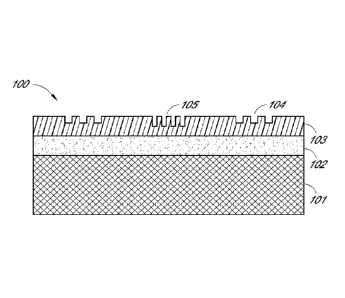
[0065] FIGs. 1A-1C illustrate the cross-section views of a substrate 100
according to
some embodiments of the present invention comprising a functionalizable layer
102 comprising
one or more functional groups; a polymer layer 103 comprising a plurality of
micro-scale or
nano-scale patterns, or combinations thereof; and a backing layer 101, where
the
functionalizable layer 102 is disposed between the backing layer 101 and the
polymer layer 103.
As shown in FIG. 1A, a substrate 100 comprises at least three layers, a
backing layer 101, a
functionalizable layer 102 and a polymer layer 103. The polymer layer 103
comprises a plurality
of nano-scale patterns 104 and 105 in different shape and depth. In some other
embodiments,
the nano-scale patterns of the polymer layer can be the same.
[0066] In some embodiments, the polymer layer has a combination of both
micro-
scale and nano-scale patterns. As shown in FIG. 1B, the polymer layer 103
further comprises a
plurality of micro-scale patterns 106 and 107, where the nano-scale patterns
104 and 105 are
formed within the micro-scale patterns. As shown in FIG. 1C, the nano-scale
structures can be
both nano-wells 104 and nano-posts 108. In FIGs. lA - 1C, the underlying
functionalizable
layer 102 is not exposed.
[0067] In some embodiments, at least a portion of the micro-scale or
nano-scale
patterns of the polymer layer perforate the polymer layer to expose the
underlying
functionalizable layer. FIG. 2A illustrate the cross-section view of a
substrate 200 according to
an embodiment of the present invention having the same layer configuration as
those described
in FIGs. 1A-1C, where the polymer layer 203 comprises nano-scale patterns 204
and 205. Nano-
scale patterns 204 perforate the polymer layer 203 to expose the underlying
functionalizable
layer 202.
[0068] In some embodiments, the functionalizable layer comprises a
plurality of
micro-scale or nano-scale patterns, or combinations thereof, and at least a
portion of the micro-
-13-
CA 02928598 2016-04-22
WO 2015/095291 PCT/US2014/070777
scale or nano-scale patterns of the polymer and functionalizable layers
perforate the polymer and
functionalizable layers to expose the underlying backing layer. FIG. 2B
depicts an substrate 200
according to another embodiment of the present invention, where the
functionalizable layer 202
comprises a plurality of nano-scale patterns 204 and 206, and nano-scale
patterns 206 perforate
the polymer layer 203 and the functionalizable layer 202 to expose the
underlying backing layer
201.
[0069] In some embodiments, as shown in FIG. 2C, each of the nano-scale
patterns
204 of the polymer layer 203 perforates the polymer layer to expose the
underlying
functionalizable layer 202.
[0070] FIG. 2D illustrates a top view of a substrate of FIG. 2B where
nano-scale
patterns 204 expose the underlying functionalizable layer 202 and nano-scale
patterns 206
perforate the polymer and functionalizable layers to expose the underlying
backing layer 201.
[0071] In some embodiments, the substrate can further comprise a sealing
layer to
substantially seal the polymer layer and the functionalizable layer between
the backing layer and
the sealing layer. As shown in FIG. 2E as a cross-section view of a substrate
according to an
embodiment of the present invention, a sealing layer 207 substantially seals
the polymer layer
203 and the functionalizable layer 202 between the sealing layer 207 and the
backing layer 201.
[0072] In some embodiments, the sealing layer can be optically
transparent. In some
embodiments, there can be some space in between the sealing layer and the
polymer layer to
allow sample fluid flowing through.
[0073] In some embodiments, the polymer layer is disposed between the
backing
layer and the fiinctionalizable layer.
[0074] FIGs. 3A-3C illustrate the cross-section views of a substrate 300
according to
some embodiments of the present invention comprising a functionalizable layer
302 comprising
one or more functional groups; a polymer layer 303 comprising a plurality of
micro-scale or
nano-scale patterns, or combinations thereof; and a backing layer 301, where
the polymer layer
303 is disposed between the functionalizable layer 302 and the backing layer
301.
[0075] As shown in FIG. 3A, a substrate 300 comprises at least three
layers, a
backing layer 301, a functionalizable layer 302 and a polymer layer 303, where
the polymer layer
303 lays in between the functionalizable layer 302 and the backing layer 301.
The polymer layer
303 comprises a plurality of nano-scale patterns 304 (nano posts) and 305
(nano wells).
[0076] In some other embodiments, the nano-scale patterns of the polymer
layer can
be uniform in size and shape.
-14-
CA 02928598 2016-04-22
WO 2015/095291 PCT/US2014/070777
[0077] In some embodiments, the polymer layer has a combination of both
micro-
scale and nano-scale patterns. As shown in FIG. 3B, the polymer layer 303
further comprises a
plurality of micro-scale patterns 306 and 307. In FIGs. 3A and 3B, the
underlying polymer layer
303 is not exposed.
[0078] FIG. 3C depicts the cross-section view of the substrate 300 of
FIG. 3A when
excess functionalizable layer 302 is removed except for those resides within
the nano-scale
patterns 304 and 305.
[0079] In some embodiments, the functionalizable layer comprises a
plurality of
micro-scale or nano-scale patterns, or combinations thereof, where at least a
portion of the
micro-scale or nano-scale patterns of the functional layer perforate the
functionalizable layer to
expose the underlying polymer layer. FIG. 4A illustrates the cross-section
view of a substrate
400 according to an embodiment of the present invention having a
functionalizable layer 402
comprising nano-scale patterns 404 and where the nano-scale patterns 404
perforate the
functionalizable layer 402 to expose the underlying polymer layer 403.
[0080] In some such embodiments, at least a portion of the micro-scale
or nano-scale
patterns of the functionalizable and polymer layers perforate the
functionalizable and polymer
layers to expose the underlying backing layer. FIG. 4B depicts a substrate 400
according to an
embodiment of the present invention, where the functionalizable layer 402 and
polymer layer
403 comprise a plurality of nano-scale patterns 406, which perforate the
polymer layer 403 and
functionalizable layer 402 to expose the underlying backing layer 401, while
nano-scale patterns
405 do not perforate the polymer layer 403. In some embodiments, the polymer
layer itself can
comprise perforated nano-scale patterns to expose the underlying backing layer
401.
[0081] In some embodiments, the substrate can further comprise a sealing
layer to
substantially seal the polymer layer and the functionalizable layer between
the backing layer and
the sealing layer. As shown in FIG. 4C, a sealing layer 407 substantially
seals the polymer layer
403 and the functionalizable layer 402 between the sealing layer 407 and the
backing layer 401.
[0082] In some embodiments, the sealing layer can be optically
transparent. In some
embodiments, there can be some space in between the sealing layer and the
functionalizable
layer to allow sample fluid flowing through.
[0083] In some embodiments, the substrate is in the shape of a cylinder.
In some
such embodiments, the backing layer is closer to an outer surface of the
cylinder than the
functionalizable or polymer layer of the substrate. In some such embodiments,
the backing layer
is closer to an inner surface of the cylinder than the functionalizable or
polymer layer of the
-15-
CA 02928598 2016-04-22
WO 2015/095291 PCT/US2014/070777
substrate. In some embodiments, a sample fluid can flow through the inner
surface of the
cylinder substrate along its longitudinal axis.
[0084] FIGs. 5A, 5B, 6A and 6B are radial cross-section views of
substrates 500 and
600 according to some embodiments of the present invention in the shape of a
cylinder. As
shown in FIG. 5A, a backing layer 501 is closer to an outer surface of the
cylinder than the
functionalizable layer 502 or polymer layer 503 of the substrate 500. Further,
the
functionalizable layer 502 comprises a plurality of nano-scale patterns 504
and 505. Nano-scale
patterns 504 perforate the polymer layer 503 to expose the underlying
functionalizable layer 502.
Nano-scale patterns 505 perforate the polymer layer 503 and the
functionalizable layer 502 to
expose the underlying backing layer 501. In FIG. 5B. the backing layer 501 is
closer to an inner
surface of the cylinder than the functionalizable layer 502 or polymer layer
503 of the substrate
500.
[0085] Similarly, FIG. 6A illustrate a substrate 600 according to an
embodiment of
the present application with a backing layer 601 is closer to an outer surface
of the cylinder than
the functionalizable layer 602 or polymer layer 603 of the substrate 600.
Further, the
funetionalizable layer 602 comprises a plurality of nano-scale patterns 604
and 605. Nano-scale
patterns 604 perforate the functionalizable layer 602 to expose the underlying
polymer layer 603
and nano-scale patterns 605 perforate the polymer layer 603 and
functionalizable layer 602 to
expose the underlying backing layer 601. In FIG. 6B, the backing layer 601 of
the substrate 600
according to an embodiment of the present application is closer to an inner
surface of the
cylinder than the functionalizable layer 602 or polymer layer 603 of the
substrate 600.
[0086] FIGs. 7A and 7B are cross-section views of a substrate 700
according to
some embodiments of the present application formed by two substrates, where
the polymer
layers 703 and the functionalizable layers 702 are substantially sealed in
between two backing
layers 701. In FIG. 7A, the substrate 700 is formed by stacking substrate 700a
on the distal
surface of the substrate 700b such that the distal surface of the two polymer
layers 703 are in
contact with each other (the distal surface being referenced to the backing
layer). Both
substrates 700a and 700b comprise nano-scale patterns 704 and 705 in the
polymer layers 703,
where nano-scale patterns 705 perforate the polymer layers 703 to expose the
underlying
functionalizablc layers 702.
[0087] In FIG. 7B, the substrate 700 is formed by stacking one substrate
700a on the
distal surface of another substrate 700a such that the distal surfaces of the
two functionalizable
layers 702 are within close proximity to each other (e.g. in many embodiments
the distal surfaces
are in direct contact with each other). Nano-scale patterns 706 perforate the
polymer layers 703
-16-
CA 02928598 2016-04-22
WO 2015/095291 PCT/US2014/070777
and the functionalizable layers 702 to expose the underlying backing layers
701. The spacing
between the two functional izable layers 702 can allow a sample fluid flowing
through. One or
more edges of the substrate 700 can be substantially sealed to avoid fluid
leaking.
[0088] In any of the disclosed embodiments, the substrate can further
comprise a
sealing layer to substantially seal the polymer layer and the functionalizable
layer between the
backing layer and the sealing layer. In some such embodiments, the sealing
layer is optically
transparent.
[0089] In any of the disclosed embodiments, at least one of the micro-
scale or nano-
scale patterns is capable of admitting a sample fluid.
[0090] In any of the disclosed embodiments, the substrate can further
comprise a
fluid reservoir, for example, a sample, reagent or waste reservoir.
[0091] In any of the disclosed embodiments, the micro-scale or nano-
scale patterns
of the polymer layer can comprise channels, trenches, wells, posts, or
combinations thereof In
some embodiments, at least a portion of the micro-scale or nano-scale patterns
are posts. In
some such embodiments, the posts have an average diameter of less than about
500 nm. In some
such embodiments, the posts have an average diameter of about 330 nm or less
including, for
example, less than about 300 nm, 200 nm, 100 nm, or 50 nm. In some such
embodiments, the
posts have an average height of less than about 500 nm. In some further
embodiments, the posts
have an average height of about 300 nm or less including, for example, less
than about 300 nm.
200 nm, 100 nm, or 50 nm. Alternatively or additionally to the exemplary upper
limits the
average diameter and/or average height of the posts can be at most 1 mm, 500
am, 100 am, 1
am, 500 nm, 400 nm, 300 nm, 200 nm or 100 nm. In some embodiments, the
plurality of micro-
scale or nano-scale patterns, or combinations thereof, are made by mechanical
embossing at
room temperature.
Functionalizable Layers
[0092] In any of the disclosed embodiments, the functionalizable layer
can comprise
a reactive silane layer, functionalizable hydrogel or a functionalizable
polymer. In some such
embodiments, the functionalizable layer can comprise one or more functional
groups. In some
such embodiments, the functional group can be selected from the group
consisting of optionally
substituted alkene, azide, optionally substituted amine, carboxylic acid,
optionally substituted
hydrazone, halogen, hydroxy, optionally substituted tetrazole, optionally
substituted tetrazine.
thiol, and combinations thereof In some further embodiments, the
functionalizable layer
comprises a polymer or hydrogel comprising Formula (Ia) or (Ib):
-17-
CA 2928598
0
(:).1 RA 1 A 7 R
(NH ),11H
o NH NH2
0,..._NH7 ,..NH O. NH
2
R1 R5 (JO R5 R1 (Ib)
R' is H or optionally substituted alkyl; the functional group R' is selected
from the group
consisting of azide, optionally substituted amine, optionally substituted
alkene, optionally substituted
hydrazone, carboxylic acid, halogen, hydroxy, optionally substituted
tetrazole, optionally substituted
tetrazine, and thiol; R5 is selected from H or optionally substituted alkyl;
each of the -(CH2)-p can be
optionally substituted; p is an integer in the range of 1 to 50; n is an
integer in the range of 1 to 50,000;
and m is an integer in the range of 1 to 100,000. In some such embodiments,
the functional groups
comprise azides. In some embodiments, each R' and IV is hydrogen. In some
embodiments, the
functional group R' is azide. In some embodiments, p is 5. In one embodiment,
the polymer or
hydrogel comprised in the functionalizable layer is PAZAM. Methods for making
and using PAZAM,
and other functionalizable materials that can be used in a layer of a
substrate of the present disclosure
are described in U.S. Pat. Pub!. No's. 2014/0079923 Al and 2015/0005447 Al.
[0093] Examples of reactive silanes that can be used include, but are
not limited to,
acrylate functional silanes, aldehyde functional silanes, amino functional
silanes, anhydride functional
silanes, azide functional silanes, carboxylate functional silanes, phosphonate
functional silanes,
sulfonate functional silanes, epoxy functional silanes, ester functional
silanes, vinyl functional silanes,
olefin functional silanes, halogen functional silanes and dipodal silanes with
any or none of the above
functional groups. Norbornene silanes are particularly useful and are
described, for example, in U.S.
Pat. Publ. No. 2015/0005447 Al. The choice of silane functionality can be made
based on the reactivity
of the material to which it will react. For example, amino functional silanes
react with thermoplastics
such as polyacrylate, polyamide, polyamide-imide, polybutylene terephthalate,
polycarbonate, polyether
ketone, polyethylene, polyphenylene sulfide, polysulfone, polyvinyl butyral
and polyvinyl chloride.
Vinyl and olefin functional silanes react with thermoplastics such as
polyacetal, polyethylene, and
polypropylene. Acrylate functional silanes react with thermoplastics such as
polypropylene, and
polystyrene.
[0094] In any of the disclosed embodiments, the functional groups of
the functionalizable
layer are attached to biomolecules. In some embodiments, the biomolecules are
selected from amino
acids, nucleosides, nucleotides, peptides, oligonucleotides, polynucleotides,
- 18 -
Date Recue/Date Received 2022-02-16
CA 02928598 2016-04-22
WO 2015/095291 PCT/US2014/070777
nucleic acids, proteins, or combinations thereof. In some such embodiments,
the biomolecules
are nucleic acids.
Functionalizable Layer - Hydrogels
[0095] In some embodiments, the functionalizable layer can comprise a
hydrogel.
Non-limiting examples of hydrogels can be used in the present application are
described herein.
[0096] WO 00/31148 discloses polyacrylamide hydrogels and polyacrylamide
hydrogel-based arrays in which a so-called polyacrylamide prepolymer is
formed, preferably
from acrylamide and an acrylic acid or an acrylic acid derivative containing a
vinyl group.
Crosslinking of the prepolymer may then be affected. The hydrogels so produced
are solid-
supported, preferably on glass. Functionalization of the solid-supported
hydrogel may also be
effected.
[0097] WO 0 1/01 143 describes technology similar to W000/31148 but
differing in
that the hydrogel bears functionality capable of participating in a [2+2]
photocycloaddition
reaction with a biomolecule so as to form immobilized arrays of such
biomolecules.
Dimethylmaleimide (DMI) is a particularly preferred functionality. The use of
[2+2]
photocycloaddition reactions, in the context of polyacrylamide-based
microarray technology is
also described in W002/12566 and W003/014392.
[0098] U.S. Pat. No. 6,465.178 discloses the use of reagent compositions
in
providing activated slides for use in preparing microarrays of nucleic acids;
the reagent
compositions include acrylamide copolymers.
[0099] WO 00/53812 discloses the preparation of polyacrylamide-based
hydrogel
arrays of DNA and the use of these arrays in replica amplification.
[0100] Once hydrogels have been formed, biomolecules may then be
attached to
them so as to produce molecular arrays, if desired. Attachment has been
effected in different
ways. For example, U.S. Pat. No. 6,372,813 teaches immobilization of
polynucleotides bearing
dimethylmaleimide groups to the hydrogels produced which bear
dimethylmaleimide groups by
conducting a [2+2] photocycloaddition step between two dimethylmaleimide
groups¨one
attached to the polynucleotide to be immobilized and one pendant from the
hydrogel.
[0101] Where the molecular array is formed after generation of the
hydrogel, two
strategies can be employed to achieve this end. Firstly. the hydrogel may be
modified chemically
after it is produced. A more common alternative is to effect polymerization
with a co-monomer
having a functionality primed or pre-activated to react with the molecules to
be arrayed.
-19-
CA 2928598
[0102] Alternatives to initial formation of hydrogels followed by
subsequent arraying
of molecules thereto have been described, for example, where the array is
formed at the same time
as the hydrogel is produced, This may be effected by, for example, direct
copolymerization of
acrylamide-derivatized polynucleotides. An example of this approach is
described in W001/62982
in which acrylamide-derivatized polynucleotides are mixed with solutions, of
acrylamide and
polymerization is effected directly.
[0103] Mosaic Technologies (Boston, Mass., USA) produce ACRYDITETm (an
acrylamide phosphoramidite) which can be reacted with polynucleotides prior to
copolymerization
of the resultant monomer with acrylamide.
[0104] Efimov et al. (Nucleic Acids Research, 1999, 27 (22), 4416-
4426) disclose a
further example of a simultaneous formation of hydrogel/array in which
copolymerization of
acrylamide, reactive acrylic acid derivatives and the modified polynucleotides
having 5'- or 3'-
terminal acrylamide groups is affected.
[0105] The compositions and methods set forth above and in the
references cited above
can be used in the compositions and methods set forth herein. For example, the
hydrogels can be
used as functionalizable layers in a substrate set forth herein.
Functionalizable Layer - Polymers
[0106] In some embodiments, the functionalizable layer can comprise a
polymer with
one or more functional groups that are capable of reacting with biomolecules
of interest. In some
such embodiments, the functional group can be selected from the group
consisting of optionally
substituted alkene, azide, optionally substituted amine, carboxylic acid,
optionally substituted
hydrazone, halogen, hydroxy, optionally substituted tetrazole, optionally
substituted tetrazine, thiol,
and combinations thereof. Non-limiting examples of the polymers can be used in
the present
application are described herein, including those described in U.S. Ser. No.
13/784,368 and U.S.
Pat. Pub. No. 2011/0059865.
PAZAM
[0107] In some embodiments, the polymer of Formula (Ia) or (Ib) is
also represented
by Formula (ha) or (lib):
- 20 -
CA 2928598 2019-12-16
CA 2928598
N3
(:))
ON
NH NH
OV NH2
NH 0 NH2 0 NH 0 NH2
0
in m (ha) m (IIb)
wherein n is an integer in the range of 1-20,000, and m is an integer in the
range of 1-
100,000.
[0108] In some embodiments, the functionalized molecule used for
direct conjugation
is poly(N-(5-azidoacetamidylpentyl)acrylamide-co-acrylamide) (PAZAM).
PAZAM can be
prepared by polymerization of acrylamide and Azapa (N-(5-(2-
azidoacetamido)pentyl)acrylamide)
in any ratio. In some embodiments, PAZAM is a linear polymer. In some other
embodiments,
PAZAM is a lightly cross-linked polymer. In some embodiments, PAZAM is applied
as an aqueous
solution. In some other embodiments, PAZAM is applied as an aqueous solution
with one or more
solvent additives, such as ethanol. The method for preparation different PAZAM
polymers is
discussed in details in U.S. Ser. No. 13/784,368.
Polymer Layer - Photocurable Polymer
[0109] In any of the disclosed embodiments, the polymer layer can
comprise at least
one photocurable polymer. In some embodiments, the photocurable polymer
comprises a urethane,
acrylate, silicone, epoxy, polyacrylic acid, polyacrylates, epoxysilicone,
epoxy resins,
polydimethylsiloxane (PDMS), silsesquioxane, acyloxysilanes, maleate
polyesters, vinyl ethers,
monomers with vinyl or ethynyl groups, or copolymers and combinations thereof.
[0110] In any of the disclosed embodiments, the backing layer may be,
for example, no
more than about 10 nm, 50 nm, 100 nm, 1 gm, 10 gm, 100 gm, 500 gm, 1 mm, 5 mm,
1 cm, or 10
cm in thickness. Alternatively or additionally, the backing layer is no less
than about 10 nm, 50
nm, 100 nm, 1 gm, 10 gm, 100 gm, 500 gm, 1 mm, 5 mm, 1 cm, or 10 cm in
thickness.
[0111] In any of the disclosed embodiments, the polymer layer is no
more than about
the length of a carbon-carbon bond, 1 nm, 10 nm, 50 nm, 100 nm, 1 gm, 10 gm,
100 gm, 500 gm, 1
mm, 5 mm, 1 cm, or 10 cm in thickness. In some embodiments, the polymer layer
is no
-21 -
CA 2928598 2019-12-16
CA 02928598 2016-04-22
WO 2015/095291 PCT/US2014/070777
less than about 10 mu, 50 nm, 100 nm, 1 gm, 10 gm, 100 gm, 500 gm, 1 mm, 5 mm,
1 cm, or
cm in thickness.
[0112] In any of the disclosed embodiments, the functionalizablc layer
is no more
than about the length of a carbon-carbon bond, 1 nm, 10 nm, 50 nm, 100 nm, 1
gm, 10 gm, 100
gm, 500 gm, 1 mm. 5 mm, 1 cm, or 10 cm in thickness. In some embodiments, the
functionalizable layer is no less than about 10 nm, 50 nm, 100 nm, 1 gm, 10
gm, 100 gm. 500
gm, 1 mm, 5 mm, 1 cm, or 10 cm in thickness.
[0113] Exemplary dicing tapes that can be used in a composition or
method set forth
herein include, but are not limited to, Lintec KL-3225 UV tape; Ultron
Systems, Anti-Static UV
Adhesive Plastic Film (p/n: 1043R-9.05), or AIT UVR250 (Al Technology Inc.,
Princeton
Junction, NJ). Other useful dicing tapes are commercially available from
Semiconductor
Equipment Corp. (Moorpark, CA) such as Low Tack, expandable PVC, 80 urn thick
(P/N
24213), Extra High Tack, non-expandable Polyethylene, 90 urn thick (P/N
24216), Super High
Tack, expandable Polyolefm, 85 urn thick (P/N 24339), or Super High Tack,
expandable
Polyolefin, 170 um thick (P/N 24351). The UC series of UV tapes for wafer
dicing sold by
Furukawa Electric Co., Ltd (Tokyo, Japan) are also useful.
Backing Layer
[0114] In any of the disclosed embodiments, the backing layer can be
made of a
material selected from the group consisting of silica, plastic, quartz, metal,
metal oxide, paper
and combinations thereof. In some such embodiments, the backing layer is made
of a flexible
plastic material. In some such embodiments, the flexible plastic material has
a stiffness that is
sufficient to preclude the backing layer from conforming to nano-scale or
micro-scale contours
on a solid support when the backing layer is contacted with the solid support
in a method set
forth herein. For example, the contacting between the solid support and
backing layer may occur
under sufficient pressure that a negative replicate of the nano-scale or micro-
scale contours is
transferred to an adhesive layer that is attached to the backing layer; yet
the backing layer will
have sufficient stiffness to resist deformation permanently or in some cases
even temporarily. In
some such embodiments, the backing layer is made from a roll of thin flexible
film. Non-
limiting examples of backing layers that can be used in the present
application are described
herein.
[0115] In some embodiments, backing layers used in the present
application include
silica-based materials, such as glass, fused silica and other silica-
containing materials. In some
embodiments, silica-based substrates can also be silicon, silicon dioxide,
silicon nitride, silicone
-22-
CA 02928598 2016-04-22
WO 2015/095291 PCT/US2014/070777
hydrides. In some embodiments, backing layers used in the present application
include plastic
materials such as polyethylene, polystyrene, poly(vinyl chloride),
polypropylene, nylons,
polyesters, polyearbonates and poly(methyl methaerylate). Preferred plastics
materials arc
poly(methyl methacrylate), polystyrene and cyclic olefin polymer substrates.
[0116] In some other embodiments, the backing layer can be a metal. In
some such
embodiments, the metal is gold. In some embodiments, the backing layer has at
least one
surface comprising a metal oxide. In one embodiment, the surface comprises a
tantalum oxide.
[0117] Acrylamide, enone, or acrylate may also be utilized as a backing
layer
material. Other backing layer materials can include, but are not limited to
gallium aresnide.
indium phosphide, aluminum, ceramics, polyimide, quartz, resins, polymers and
copolymers.
The foregoing lists are intended to be illustrative of, but not limited to the
present application.
[0118] In some embodiments, the backing layer and/or the backing layer
surface can
be quartz. In some other embodiments, the backing layer and/or the backing
layer surface can be
semiconductor, i.e. GaAs or ITO.
[0119] In some embodiments, the backing layer is made of paper.
[0120] In some embodiments, the backing layer is made of a flexible
material. In
some such embodiments, the backing layer is made from a roll of thin flexible
film (for example,
having a thickness of less than about 1 mm. 500 m, 100 m, or less.
[0121] Backing layers can comprise a single material or a plurality of
different
materials, for example, two or more layers of one or more materials. The shape
of the backing
layers employed may be varied in accordance with the application for which the
present
application is practiced.
Doped Layers
[0122] One or more of the layers that is present in a composition or used in a
method set
forth herein can be doped with a material having a desired characteristic. For
example, a layer
can have plasmonic properties due to the presence of nanoparticles, Q dots or
the like spiked into
the material of the layer. The resulting plasmonic properties can provide an
antenna effect
during a subsequent detection step that is carried out in or on the doped
layer. Alternatively or
additionally, a layer can be doped with receptors, ligands or nucleic acids to
provide binding
specificity in an analytical detection application; or doped with reactive
moieties, such as those
set forth herein in the context of functionalizable layers, to provide for
subsequent
functionalization; or doped with materials that alter optical properties of
the layer such as optical
filter materials, materials that absorb light in a particular wavelength
range, materials that emit
-23-
CA 2928598
light in a particular wavelength range, or materials that scatter light; or
doped with materials that
impart conductive characteristics such as electrical conductivity; or doped
with materials that are
thermally conductive.
[0123] In particular embodiments, a layer can be doped prior to use in
a method set
forth herein. For example, one or more layer of a substrate can be doped prior
to creation of a
pattern in the substrate. By way of more specific example, a polymer layer or
functionalizable
layer can be doped prior to creation of a pattern in the polymer layer. As
such, the dopant material
in the polymer layer will form part of the pattern, being displaced from some
regions of the pattern
and retained in other regions of the pattern. A dopant material that is in a
functionalizable layer can
be exposed in some portions of the pattern and protected in other parts of the
pattern to allow for
selective detection or reactivity of the exposed portions in a subsequent use
of the substrate.
[0124] One or more of the layers set forth herein can be doped,
including, for example,
a polymer layer, functionalizable layer, or backing layer. The dopant material
can be present
primarily or solely on the surface of a layer, within the volume of a layer,
or both within the layer
and on the surface of the layer.
Substrate Applications
[0125] In some embodiments, a substrate described herein forms at
least part of a flow
cell or is located in a flow cell. In some such embodiments, the flow cells
further comprise
polynucleotides attached to the surface of the substrate via reaction with the
functional groups of
the functionalizable layer, for example, a hydrogel coating. In some
embodiments, the
functionalizable layer is disposed between the polymer layer and the backing
layer, with at least a
portion of the micro-scale or nano-scale patterns of the polymer layer are
perforated to expose the
underlying functionalizable layer. In some embodiments, the polymer layer is
disposed between
the functionalizable layer and the backing layer, with at least a portion of
the micro-scale or nano-
scale patterns of the functionalizable layer are perforated to expose the
underlying polymer layer.
[0126] In some embodiments, the polynucleotides are present in the
flow cells in
polynucleotide clusters, wherein the polynucleotides of the polynucleotide
clusters are attached to a
surface of the flow cell via the hydrogel coating. Clusters can be formed by
solid-phase
amplification techniques such as solid-phase PCR, bridge amplification or
other techniques known
in the art or described in U.S. Pat. No. 5,641,658; U.S. Patent Publ. No.
2002/0055100; U.S. Pat.
No, 7,115,400; U.S. Patent Publ. No. 2004/0096853; U.S. Patent Publ. No.
2004/0002090; U.S.
- 24 -
CA 2928598 2019-12-16
. .
CA 2928598
Patent Pub!. No. 2007/0128624; and U.S. Patent Pub!. No. 2008/0009420. In
preferred
embodiments, the flow cell is a flow chamber that is divided into a plurality
of lanes or a plurality
of sectors, wherein one or more of the plurality of lanes or plurality of
sectors comprises a surface
that is coated with a covalently attached functionalizable hydrogel coating
described herein. In
some embodiments of the flow cells described herein, the attached
polynucleotides within a single
polynucleotide cluster have the same or similar nucleotide sequence. In some
embodiments of the
flow cells described herein, the attached polynucleotides of different
polynucleotide clusters have
different or nonsimilar nucleotide sequences. Exemplary flow cells and
substrates for manufacture
of flow cells that can be used in method or composition set forth herein
include, but are not limited
to, those commercially available from Illumina, Inc. (San Diego, CA) or
described in US
2010/0111768 Al or US 2012/0270305.
[0127] In some embodiments, a substrate described herein forms
at least part of a
microfluidic device or is located within a microfluidic device. Exemplary
devices include flow
cells useful in nucleic acid sequencing and other analytical procedures such
as the flow cells
commercially available from Illumina, Inc. (San Diego, CA) or described in
U.S. 2010/0111768 Al
or U.S. 2012/0270305 Al. Other microfluidic devices include cell sorting
devices, lab on a chip
devices, capillary sequencers, cell counting devices and the like can also be
prepared at least in part
from a substrate described herein or comprise a substrate described herein.
Substrates Preparation
[0128] Some embodiments disclosed herein include a process for
preparing a substrate,
comprising: providing a substrate comprising a functionalizable layer
comprising one or more
functional groups disposed between a backing layer and a layer of photocurable
polymer;
contacting a surface of the layer of photocurable polymer with a template
having a plurality of
micro-scale or nano-scale patterns including micro-scale or nano-scale wells,
posts, channels,
junctions or combinations thereof; applying pressure to the template or
substrate to transfer the
micro-scale or nano-scale patterns to at least the layer of photocurable
polymer, where the
contacting and applying are performed at room temperature; irradiating the
photocurable polymer
with UV light to cure the photocurable polymer; and separating the template
from substrate; where
at least a portion of the polymer layer is perforated to expose the underlying
functionalizable layer.
[0129] FIGs. 8A - 8D are cross-section views to illustrate a
UV nano-embossing
process to prepare a substrate 800 according to an embodiment of the present
invention.
- 25 -
CA 2928598 2019-12-16
CA 02928598 2016-04-22
WO 2015/095291 PCT/US2014/070777
[0130] In FIG. 8A, an embossed stamp 804 comprises a plurality of nano-
scale
patterns 805 and 806 thereon, and a plurality of grooves 807 in between the
nano-scale patterns.
A substrate 800 comprising a backing layer 801, a functionalizable layer 802
and a photocurable
polymer layer 803a is also provided.
[0131] Next, the embossed stamp 804 is contacted with an upper surface
of the
photocurable polymer layer 803a, then pressure is applied to the embossed
stamp 804 or the
substrate 800 as shown in FIG. 8B. The nano-scale patterns 805 and 806 are
formed in the
photocurable polymer layer 803a of the substrate 800.
[0132] Then, UV light is irradiated onto the UV curable polymer layer
803a through
the embossed stamp 804 as shown in FIG. SC. The embossed stamp 804 is made of
a material
that allows UV light to pass through such that UV light reaches the
photocurable polymer layer
803a and cure the photocurable polymer, forming a polymer layer 803.
Alternatively, the UV
light can be applied through the backing layer 801 if the backing layer and
functionalizable layer
802 are made of materials that allow UV light to pass through.
[0133] Next, the embossed stamp 804 is separated from the polymer layer
803
resulting in the formation of nano-scale patterns 805 and 806 in the substrate
800 as shown in
FIG. 8D. Nano-scale patterns 805 perforate the polymer layer 803 to expose the
underlying
functionalizable layer 802.
[0134] Some embodiments disclosed herein include a process for preparing
a
substrate, comprising: providing a template comprising a plurality of micro-
scale or nano-scale
patterns including micro-scale or nano-scale wells, channels or combinations
thereof on a
surface of the template; depositing a functional layer comprising one or more
functional groups
on the surface of the template such that at least a portion of the micro-scale
or nano-scale wells,
channels or combinations thereof contain the functional layer: removing excess
functionalizable
layer from the surface of the template such that the functionalizable layer is
present on only a
portion of the template surface; providing a substrate comprising a backing
layer having a
photocurable polymer layer disposed on the backing layer; contacting a surface
of the
photocurable polymer layer with the surface of the template having the
plurality of micro-scale
or nano-scale patterns and functionalizable layer thereon; applying pressure
to the template or
substrate to transfer the micro-scale or nano-scale pattern to at least the
layer of photocurable
polymer, where the contacting and applying are performed at room temperature;
irradiating the
photocurable polymer with UV light to cure the photocurable polymer; and
separating the
template from the substrate; where at least a portion of the functionalizable
layer is transferred to
the polymer layer.
-26-
CA 02928598 2016-04-22
WO 2015/095291 PCT/US2014/070777
[0135] FIGs. 9A - 9E are cross-section views to illustrate a UV nano-
embossing
process to prepare a substrate 900 according to an embodiment of the present
invention.
[0136] In FIG. 9A, an embossed stamp 904 comprises a plurality of nano-
scale
patterns 905 thereon, and a plurality of grooves 906 in between the nano-scale
patterns 905. A
functionalizable layer 902 is deposited on the nano-scale patterned surface of
the embossed
stamp 904.
[0137] Next, in FIG. 9B, excess functionalizable layer 902 is removed
such that the
functionalizable layer is only present within the nano-scale patterns 905 of
the embossed stamp
904. A substrate 900a having a backing layer 901 and a photocurablc polymer
layer 903a is
provided.
[0138] Then, the embossed stamp 904 is contacted with an upper surface
of the
photocurable polymer layer 903a, and then pressure is applied to the embossed
stamp 904 or the
substrate 900a as shown in FIG. 9C. The nano-scale patterns 905 are formed in
the
photocurable polymer layer 903a of the substrate 900a.
[0139] Next, UV light is irradiated onto the UV curable polymer layer
903a through
the embossed stamp 904 as shown in FIG. 9D. The embossed stamp 904 is made of
a material
that allows UV light to pass through such that UV light reaches the
photocurable polymer layer
903a and cure the photocurable polymer, forming a polymer layer 903.
Alternatively, the UV
light can be applied through the backing layer 901 if the backing layer 901 is
made of materials
that allow UV light to pass through.
[0140] Finally, the embossed stamp 904 is separated from the polymer
layer 903. The
functionalizable layer 902 is transferred to the top surface of the polymer
layer 903. In addition,
nano-scale patterns 905 are formed in the polymer layer 903 as shown in FIG.
9E.
[0141] In some embodiments, the embossed stamp can have micro-scale or
nano-
scale patterns that result in at least a portion of polymer layer and
functionalizable layer being
perforated to expose the underlying backing layer.
[0142] In some embodiments, the substrate further comprises a backing
layer having
a photocurable polymer layer disposed on the backing layer is a roll of
flexible dicing tape.
10143J In any of the disclosed process embodiments, the process can
further
comprises applying a sealing layer to the substrate after removing the
template to substantially
seal the polymer layer and the functionalizable layer between the backing
layer and the sealing
layer.
[0144] In some embodiments, the sealing layer further comprises a second
substrate
prepared by the process of any of the disclosed embodiments, where the
functionalizable layers
-27-
CA 02928598 2016-04-22
WO 2015/095291 PCT/US2014/070777
and photocurable polymer layers of the substrates are disposed between the
backing layers of the
substrates. In some such embodiments, the sealing layer is optically
transparent.
[0145] In any of the disclosed process embodiments, the process can
further
comprise forming the substrate into a cylinder. In some embodiments, the
backing layer is closer
to an outer surface of the cylinder than the functionalizable or polymer layer
of the substrate. In
some other embodiments, the backing layer is closer to an inner surface of the
cylinder than the
functionalizable or polymer layer of the substrate. In some embodiments, the
cylindrical shaped
substrate can be formed using a flexible backing layer and wrapping the
substrate around a
cylindrical object, such as a glass or plastic rod or capillary.
[0146] In any of the disclosed process embodiments, the process can be a
roll to roll
process.
[0147] From the foregoing, it will be appreciated that various
embodiments of the
present disclosure have been described herein for purposes of illustration,
and that various
modifications can be made without departing from the scope and spirit of the
present disclosure.
Accordingly, the various embodiments disclosed herein are not intended to be
limiting, with the
true scope and spirit being indicated by the following claims.
EXAMPLES
[0148] Additional embodiments are disclosed in further detail in the
following
examples, which are not in any way intended to limit the scope of the claims.
Example 1
High Fidelity Nano-scale Patterns Transfer
[0149] An 8" master template wafer containing 12 Hi-seq sized patterned
flowcells
was used to emboss directly into a UV curable adhesive coated polymer sheet
(FIG. 10A). The
template wafer with nano-scale patterned structures was aligned with a polymer
sheet coated
with a UV curable adhesive layer such that the adhesive layer was in direct
contact with the nano
patterned surface. Mechanical force was applied on the polymer sheet's non-
adhesive surface.
Then the polymer sheet was irradiated with UV light to cure the adhesive and
the polymer sheet
was released by &lamination. As a result, high fidelity pattern transfer from
the template to the
polymer sheet was observed. Diffraction patterns from flowcell regions confirm
large area
pattern transfer.
[0150] Flowcell 7 (FC7) was cut out of the polymer sheet for further
microscope
inspection and electron microscopy. As shown in FIG. 10B, dark field
microscope image of a
fiducial from FC7 confirms nano-scale patterns transfer. The master template
in this case
-28-
CA 02928598 2016-04-22
WO 2015/095291 PCT/US2014/070777
contained 350 nm nano-well features with 750 nrn pitch. The pattern
transferred into the
polymer sheet was the opposite polarity as the pattern in the template (nano-
posts).
Furthermore. SEM images of fiducial region of the FC7 at 1240X and 20kX
magnifications arc
illustrated in FIGs. 10C and 1011. In addition, nano-scale pillars on polymer
sheet at 40 kX and
80 kX magnifications are illustrated in FIGs. 10E and 10F. Excellent pattern
transfer was seen
in all cases with post diameters in the range of about 330 nm and a post-
height of about 300 nm.
Example 2
High Fidelity Reverse Polarity Nano-scale Patterns Transfer
[0151] The polarity of nano-scale patterns of the master template was
reversed as
compared to the master template described in Example I. The master template
comprises nano-
scale posts instead of nano-well features. The same pattern transfer process
as described in
Example l was used to generate the opposite polarity pattern on the polymer
sheet. The
formation of nano-wells and nano-trenches in the polymer sheet following
physical embossing
and UV curing are shown in FIGs. 11A and 11B with different magnification.
High fidelity,
high throughput pattern transfer was achieved.
Example 3
High Throughput Embossing of Microfluidic Structures
[0152] A silicon master template comprising microfluidic structures in
patterned SU-
8 photoresist was prepared. Then the silicon master wafer was imprinted into a
clear polymer
sheet with a UV curable adhesive layer such that the microfluidic pattern was
in direct contact
with the adhesive layer. After standard UV radiation and release process as
described in
Example I, multiple 4-inch polymer replicas of the master wafer were formed in
less than 2
minutes. The patterned microfluidic structures transferred are shown in FIGs.
12A-12D. These
fluidic structures were formed in commercially available dicing tape (Lintee
KL-3225 UV tape
or Ultron Systems, Anti-Static UV Adhesive Plastic Film p/n: 1043R-9.05).
[0153] FIG. 12A depicts serpentine fluidic channels and junctions formed
for
applications such as fluidic mixing. Similarly, Microfluidic filters (FIG.
12B) was formed for
applications such as cell capture, separation or size dependent sorting.
Furthen-nore, the
microfluidic structures was tested by using capillary driven fluid (1M NaCI
with red dye)
flowing through a serpentine microfluidic channel. FIG. 12C illustrates an
optical image of the
fluid flowed through the microfluidic channel at different time point (t= 5s
and t=10s). FIG.
1211 shows an optical image of the fluid flowed into a T-junction for fluid
mixing.
-29-