Note: Descriptions are shown in the official language in which they were submitted.
CA 02930188 2016-05-10
WO 2015/070344
PCT/CA2014/051065
1
COMPENSATION CIRCUIT, COMMUTATION CELL AND
POWER CONVERTER CONTROLLING TURN-ON AND TURN-
OFF OF A POWER ELECTRONIC SWITCH
TECHNICAL FIELD
[0001] The present disclosure relates to the field of power
electronics.
More specifically, the present disclosure relates to a compensation circuit, a
commutation cell and a power converter controlling turn-on and turn-off of a
power electronic switch.
BACKGROUND
[0002] Commutation cells are commonly used in electronic systems
that require conversion of a voltage source, including both DC-DC converters
and DC-AC converters, which are often called inverters. With the limited space
allowed for power converter circuits, such as those used for example in
electric
and/or electric hybrid automotive applications, and given the high cost of the
semi-conductors, the demand for integration of these commutation cells
increases.
[0003] A known way of reducing the space occupied by
semiconductors in power converter circuits is to increase their efficiency to
thereby allow the size of their cooling surface to be reduced.
[0004] Losses in power electronic switches present in conventional
power converter circuits are mainly caused by two sources; conduction losses
and switching losses. One way to reduce switching losses is generally by
accelerating the turn-on and turn-off of the power electronic switches.
However, fast turn-off of the power electronic switches generates overvoltage
in parasitic (stray) inductances of their high-frequency loop. It is thus
often
required to slow down turning off of the power electronic switches to protect
them against overvoltage. This may seriously impact the overall efficiency of
conventional power converter circuits.
CA 02930188 2016-05-10
WO 2015/070344
PCT/CA2014/051065
2
[0005] Figure 1 is an idealized circuit diagram of a conventional
commutation cell such as those used in conventional power converter circuits.
A commutation cell 10 converts a DC voltage Vbõ, from a voltage source 12 (or
from a capacitor) into a current source /out (or into an inductance) that
usually
generates a voltage Võt appropriate for a load 14, which may be a resistive
load, an electric motor, and the like. The commutation cell 10 comprises a
freewheel diode 16 and a controlled power electronic switch 18, for example
an isolated gate bipolar transistor (IGBT). A capacitor 20 (Cm) is used to
limit
variations of the voltage Vbõ of the voltage source 12 and an inductance 32 is
used to limit the variations of the output current /out. A gate driver (not
shown in
Figure 1 but shown on later Figures) controls turning on and off of the power
electronic switch 18. Figure 1 illustrates a configuration of the commutation
cell
10, of the load 14, and of the voltage source 12, in which energy flows from
the
voltage source 12 to the load 14, i.e. from left to right on the drawing. The
commutation cell 10 can also be used in a reverse configuration in which
energy flows in the opposite direction.
[0006] When turned on, the power electronic switch 18 allows current
to pass therethrough, from its collector 22 to its emitter 24; at that time,
the
power electronic switch 18 can be approximated as a closed circuit. When
turned off, the power electronic switch 18 does not allow current to pass
therethrough and becomes an open circuit.
[0007] The gate driver applies a variable control voltage between the
gate 26 and the emitter 24 of the power electronic switch 18. For some types
of power electronic switches such as bipolar transistors, the gate driver may
act as a current source instead of as a voltage source. Generally, when the
voltage applied between the gate 26 and the emitter 24 is "high", the power
electronic switch 18 allows passing of current from the collector 22 to the
emitter 24. When the voltage applied between the gate 26 and the emitter 24 is
"low", the power electronic switch 18 blocks passage of current therethrough.
In more details, a voltage difference between the gate 26 and the emitter 24,
CA 02930188 2016-05-10
WO 2015/070344
PCT/CA2014/051065
3
denoted Vge, is controlled by the gate driver. When Vge is greater than a
threshold Vge(th) for the power electronic switch 18, the switch 18 is turned
on
and a voltage Võ between the collector 22 and the emitter 24 becomes near
zero. When Vge is lower than Vge(th), the power electronic switch 18 is turned
off
and lice eventually reaches V.
[0008] When the power electronic switch 18 is turned on, a current
lout
flows from the voltage source 12 (and transiently from the capacitor 20)
through the load 14 and through the collector 22 and the emitter 24. When the
power electronic switch 18 is turned off, the current 'out circulates from the
load
14 and passes in the freewheel diode 16. It may thus be observed that the
power electronic switch 18 and the freewheel diode 16 operate in tandem.
Turning on and off of the power electronic switch 18 at a high frequency
allows
the current 'out, in the output inductance Lut 32, to remain fairly constant.
[0009] It should be observed that, in the case of other power
electronic switch types, for example bipolar transistors, the term "gate" may
be
replaced with "base", the base being controlled by a current as opposed to the
gate that is controlled by a voltage. These distinctions do not change the
overall operation principles of the commutation cell 10.
[0010] Figure 2 is another circuit diagram of the conventional
commutation cell of Figure 1, showing parasitic (stray) inductances. In
contrast
with the idealized model of Figure 1, connections between components of an
actual commutation cell define parasitic inductances. Though the parasitic
inductances are distributed at various places within the commutation cell 10,
a
suitable model presented in Figure 2 shows two (2) distinct inductances
representing the overall parasitic inductance, including an emitter inductance
30 of the power electronic switch 18 and an inductance 34 representative of
all
other parasitic inductances (other than the emitter inductance 30) around a
high frequency loop 36 formed by the freewheel diode 16, the power electronic
switch 18 and the capacitor 20. The high frequency loop 36 is a path where
current changes significantly upon switching of the power electronic switch
18.
CA 02930188 2016-05-10
WO 2015/070344
PCT/CA2014/051065
4
It should be noted that an output inductance Lõt 32 is not part of the high
frequency loop because its current remains fairly constant through the
commutation period.
[0011] Figure 3 is a circuit diagram of a conventional commutation
cell further showing a gate driver 40. Some elements of the commutation cell
are not shown on Figure 3, in order to simply the illustration. Figure 3
further shows a gate driver 40 having a positive supply voltage 42 and a
negative supply voltage 44, an output 46 of the gate driver 40 being connected
to the gate 26 of the power electronic switch 18 via a gate resistor Rg. The
positive supply voltage 42 of the gate driver 40 has a value denoted +14,
while
the negative supply voltage 44 has value denoted -Vdd. An input 48 of the gate
driver 40 is connected to a controller (not shown) of the commutation cell 10,
as is well known in the art. A voltage at the output 46 of the gate driver 40
goes
up to +14, and goes down to -Vdd in order to control the voltage at the gate
26.
The input resistance of the gate 26 to emitter may be very high, especially in
the case of an IGBT. However, a parasitic Miller capacitance present between
the gate 26 and the emitter 24, causes some current to flow from the output 46
when the gate driver 40 alternates between +14, and -Vdd. The value Rg of the
gate resistor is selected as a function of the parasitic Miller capacitance
and of
a desired switching rate of the power electronic switch 18 so that the voltage
at
the gate 26 changes at rate appropriate for the desired switching rate.
[0012] On Figure 3, a current /igbt flowing through the power
electronic
switch 18 and through the emitter parasitic inductance 30 is essentially equal
to 'out when the power electronic switch 18 is turned on, and quickly reduces
to
zero (substantially) when the power electronic switch 18 turns off.
[0013] When the power electronic switch 18 turns on or off, the
current Lot flowing therethrough increases or diminishes at a fast rate. These
variations of Lot, denoted di/dt, generate voltage across inductances 30 and
34, according to the well-known equation (1):
CA 02930188 2016-05-10
WO 2015/070344
PCT/CA2014/051065
di
= L = ¨ (1)
dt
[0014] wherein VL is a voltage induced across an inductance and L is
an inductance value.
[0015] A voltage VL, is generated across the parasitic inductance 34
and a voltage VL, is generated across the emitter parasitic inductance 30. On
Figures 2 and 3, the polarities shown across the high frequency loop
inductance 34, including the emitter inductance 30 reflect voltages obtained
upon turn-off of the power electronic switch 18, when the iigbt current
diminishes very rapidly, di/dt thus taking a negative value. Upon turn-on of
the
power electronic switch 18, voltages across the high frequency loop
inductance 34, including the emitter inductance 30 are in the opposite
direction.
[0016] These voltages VL, and VL, are in series with Vbõ from the
voltage source 12. When the power electronic switch 18 turns off, the
collector
22 to emitter 24 voltage increases until the freewheel diode 16 turns on. At
that
time, addition of Vbõ, VL, and VL, results in an important overvoltage applied
between the collector 22 and the emitter 24 of the power electronic switch 18.
Though power electronic switches are rated for operation at some level of
voltage, extreme overvoltage can reduce the lifetime of any power electronic
switch to thereby lead to its premature failure or even break the device.
[0017] Figure 4 is a circuit diagram of a conventional !GET leg formed
of two conventional commutation cells. Two commutation cells 10 introduced in
the above description of Figures 1-3, in which IGETs are used as power
electronic switches 18 in the example of Figure 4, are connected in a single
loop to form an !GET leg 70 of a power converter 50. A first power electronic
switch (bottom !GET Q1) operates in tandem with a first freewheel diode (top
freewheel diode D2) and a second power electronic switch (top IGBT Q2)
operates in tandem with another freewheel diode (bottom freewheel diode D1).
Each !GET has its own gate driver 40. A voltage source 12 provides a voltage
CA 02930188 2016-05-10
WO 2015/070344
PCT/CA2014/051065
6
Vbus in parallel to an input capacitance 20 (Cm) connected to the IGBT leg 70
via a parasitic inductance L. Parasitic inductances inherently provided in
wires, connections, decoupling capacitor and circuit board traces of a power
converter have been represented in Figure 4. A three-phase power converter
used for powering a three-phase electric motor (not shown) from a battery
such as 12, would comprise three (3) IGBT legs 70 as shown on Figure 4.
Since such three-phase power converters are believed well-known, they are
not described in further details herein.
[0018] As can be seen from Figure 4, a reference of each gate driver
is connected to the emitter of the IGBT Q1 and Q2, typically known as logical
pins of the IGBTs Q1 and Q2. For concision purpose, a description of Figure 4
focuses on its bottom portion including the bottom IGBT Q1.
[0019] The overvoltage effect on a power electronic switch 18,
discussed in the above description of Figures 2 and 3, also applies to the
IGBTs Q/ and Q2.
[0020] When the bottom IGBT Q1 is turned off, current transits from
the bottom IGBT Q1 to the top freewheel diode D2, during an overvoltage
period. A properly selected IGBT is able to support the overvoltage created by
a current variation (di/dt) across various parasitic inductances (Lc, L+Vbus,
Lc-high,
Le-high, Lc-low, Le-low and L-vbus) present in the IGBT leg 70. Indeed, since
the
inductances resist change of current therein, additive voltages develop in the
IGBT leg 70 as illustrated by the polarities of the parasitic inductances
shown
on in Figure 4. These voltages, added to the voltage Vbus of the source, often
result in a voltage exceeding the maximal collector to emitter voltage lice
rating
of the bottom IGBT Q1. The top IGBT Q2 is subject to the same problem.
[0021] Solutions exist that tend to limit overvoltage in power
electronic
switches by slowing down the slope of the gate-emitter voltage. However,
excessive limitation of the overvoltage can imply longer switching times of
the
current, reducing commutation cell performance.
CA 02930188 2016-05-10
WO 2015/070344
PCT/CA2014/051065
7
[0022] Also, the commutation cell 10 and the power converter 50 can
deliver their maximum power when operating at high bus voltages V.
Current solutions to limit the overvoltage generated across the parasitic
inductances of the high frequency loop 36 allow using bus voltages
approaching the maximum voltage rating of the power electronic switches 18.
However, bus voltages may vary over time or between different applications.
For those reasons, overvoltage protection in conventional commutation cells
generally need to be overdesigned, as a safety measure, As such,
conventional commutation cells operate at less than their maximum attainable
power output.
[0023] Numerous additional problems related to dynamic current
sharing arise from parallelization of commutation cells, particularly when
placing IGBT legs in parallel. For example, should one of a pair of
parallelized
power electronic switch transition being states faster than the other of the
same pair, this fastest switch supports more current than the others and
therefore generates more heat. This often leads to premature ageing of some
of the parallelized power electronic switches, leading to the premature end of
life of power converters.
[0024] Conventionally, to overcome such dynamic unbalance
problems, some rules are followed. A first rule suggests using a matching gate
driver circuit for each power electronic switch, in which gate drivers having
equal gate resistors as well as gate loop inductance are used to minimize the
delays between the switching times of all the power electronic switches.
According to a second rules, power electronic switches to be placed in
parallel
are selected so that they have matched intrinsic parameters, such as parasitic
capacitances, threshold voltage and gain. Selection of matched power
electronic switches may be made by using switches manufactured in a same
batch. Finally, a third rule suggests using identical circuit layouts in the
high
frequency loop for every power electronic switch.
[0025] It is often particularly difficult to fulfill this third rule,
in many
CA 02930188 2016-05-10
WO 2015/070344
PCT/CA2014/051065
8
applications, since common power electronic switch have their own power
circuit paths. Also, when placing discrete switches in parallel, it is not
always
possible to match each of their power circuit branches because of mechanical
and packaging imperatives.
[0026] Therefore, there is a need for circuits capable of compensating
for variable characteristics of power electronic switches.
SUMMARY
[0027] According to the present disclosure, there is provided a
compensation circuit for independently controlling turn-on and turn-off of a
power electronic switch through a gate driver. The compensation circuit
includes a first circuit path configured to sample a first portion of a
voltage
induced across an inductance of the power electronic switch at turn-on of the
power electronic switch. Also included is a second circuit path configured to
sample a second portion of the voltage induced across the inductance of the
power electronic switch at turn-off of the power electronic switch. The
compensation circuit further includes a gate driver reference connection
configured to respectively supply the first and second portions of the voltage
during turn-on and turn-off of the power electronic switch.
[0028] The present disclosure also relates to a compensation circuit
for independently controlling turn-on and turn-off of a first power electronic
switch that is placed in parallel with a second power electronic switch, the
control being done through a gate driver. The compensation circuit includes a
first circuit path configured to sample a first portion of a voltage induced
across
an inductance of the first power electronic switch at turn-on of the first
power
electronic switch. Also included is a second circuit path configured to sample
a
second portion of the voltage induced across the inductance of the first power
electronic switch at turn-off of the first power electronic switch. The
compensation circuit further includes a gate driver reference connection
configured to respectively supply the first and second portions of the voltage
CA 02930188 2016-05-10
WO 2015/070344
PCT/CA2014/051065
9
during turn-on and turn-off of the first power electronic switch.
[0029] According to the present disclosure, there is also provided a
commutation cell configured for limiting switching overvoltage. The
commutation cell comprises a power electronic switch having a parasitic
inductance through which a voltage is generated upon turning on and off of the
power electronic switch and the compensation, which is connected to the
parasitic inductance.
[0030] The present disclosure further relates to a power converter,
comprising a pair of parallel legs, each leg having a pair of power electronic
switches connected in series, each power electronic switch being provided with
one of the compensation circuits.
[0031] The present disclosure also relates to a power converter,
comprising a pair of parallel legs, each leg connecting in series a pair of
the
commutation cells that include the compensation circuit.
[0032] The foregoing and other features will become more apparent
upon reading of the following non-restrictive description of illustrative
embodiments thereof, given by way of example only with reference to the
accompanying drawings.
BRIEF DESCRIPTION OF THE DRAWINGS
[0033] Embodiments of the disclosure will be described by way of
example only with reference to the accompanying drawings, in which:
[0034] Figure 1 is an idealized circuit diagram of a conventional
commutation cell such as those used in conventional power
converter circuits;
[0035] Figure 2 is another circuit diagram of the conventional
commutation cell of Figure 1, showing parasitic (stray)
inductances;
[0036] Figure 3 is a circuit diagram of a conventional commutation
CA 02930188 2016-05-10
WO 2015/070344
PCT/CA2014/051065
cell further showing a gate driver;
[0037] Figure 4 is a circuit diagram of a conventional IGBT leg
formed
of two conventional commutation cells;
[0038] Figure 5 is a circuit diagram of a power converter including
two
parallelized IGBT legs;
[0039] Figure 6 is a detailed view of a portion of Figure 5
illustrating a
compensation circuit according to a first illustrative
embodiment; and
[0040] Figure 7 is a detailed view of a portion of Figure 5
illustrating a
compensation circuit according to a second illustrative
embodiment.
[0041] Like numerals represent like features on the various drawings.
DETAILED DESCRIPTION
[0042] Various aspects of the present disclosure generally address
one or more of the problems related to variable characteristics of power
electronic switches.
[0043] Circuits operable to limit overvoltage in commutation cells,
especially at turn-off of IGBTs, are described in international patent
publication
no WO 2013/082705 Al, in international patent application no
PCT/CA2013/000805, in US provisional applications no 61/808,254, no
61/898,502, no 61/904,038, no 61/905,045 and no 61/904,050, and in
"Reducing switching losses and increasing IGBT drive efficiency with ReflexTM
gate driver technology", available at
http://www.advbe.com/docs/DeciElec2013-Jean Marc Cyr-TM4.pdf, all of
which are authored by Jean-Marc Cyr et al. the disclosure of these being
incorporated by reference herein.
[0044] The present technology provides control of overvoltage and
switching losses at turn-off and turn-on of a power electronic switch of a
CA 02930188 2016-05-10
WO 2015/070344
PCT/CA2014/051065
11
commutation cell. Circuits and methods presented herein are generally
compatible with other solutions to limit overvoltage at turn-off and/or turn-
on of
parallelized power electronic switches. Without limitation, the disclosed
technology may be used in a single commutation cell, in a leg having two (2)
cascaded commutation cells, and in parallelized legs.
[0045] In a commutation cell, di/dt at turn-off of a power electronic
switch generates a voltage across parasitic (stray) inductances of a high
frequency loop of the commutation cell. This voltage is applied across the
power electronic switch in addition to a bus voltage providing power to the
commutation cell. A solution based on the injection of a sample of the
overvoltage present across the power electronic switch to a gate driver of the
power electronic switch has been proposed. A commutation cell built according
to the present disclosure comprises a pair of circuit paths that respectively
select a different portion of a voltage induced across an inductance of a
power
electronic switch at turn-on and at turn-off of the power electronic switch so
that these portions are selectively applied to control the turn-on and turn-
off of
the power electronic switch.
[0046] The techniques disclosed herein will mainly be described in
relation to power converters including pairs of commutation cells forming IGBT
legs, a pair of IGBT legs being further placed in parallel for high power
applications. The same teachings are however applicable to single
commutation cells or to single IGBT legs. Additionally, the following
description
will mainly relate to the use of isolated gate bipolar transistors (IGBT).
Mentions of IGBTs in the following description are made for illustration
purposes and are not meant to limit the present disclosure. The same
techniques may equally be applied to commutation cells constructed using
metal¨oxide¨semiconductor field-effect transistors (MOSFET), bipolar
transistors and like power electronic switches.
[0047] Generally stated, the disclosed compensation circuit
facilitates
parallel operation of power electronic switches described herein by the
CA 02930188 2016-05-10
WO 2015/070344
PCT/CA2014/051065
12
reduction of dynamic unbalance between parallelized power electronic
switches having distinct characteristics. This is accomplished by balancing
the
switched currents at turn-on and turn-off. A compensation circuit is provided
to
inject a feedback of a drop voltage across the parasitic inductance of the
high
frequency loop of each individual power electronic switch to its respective
gate
driver circuit. This allows to selectively adjust the speed at turn-on and
turn-off
of the parallelized switches. This compensation circuit separately adjusts the
current variation (di/dt) in the commutation cell by dynamically decreasing a
voltage applied at the gate of the power electronic switch during the turn-on
and by increasing it during turn-off. Of course, the disclosed compensation
circuit may be used in single power electronic switch configurations, or in
single leg configurations, as it offers an alternative solution to the general
problem of overvoltage control during switching.
[0048] Figure 5 is a circuit diagram of a power converter including
two
parallelized IGBT legs. Figure 5 also illustrates the parasitic inductances
caused by the components interconnections as well as individual feedback
loops to the gate driver of each power electronic switch. In the example of
Figure 5, the two legs could be constructed from discrete parts or from
switches of a same module or of different modules. In the context of the
present disclosure, a 'module' is a package containing chips including several
IGBTs and diodes, made from a common wafer. The two parallelized switches
could be also discrete parts to be parallelized to increase the available
phase
current at the output.
[0049] The first leg 100 includes a bottom IGBT Q1, its associated
freewheel diode D2 and parasite inductances Lc1-10w and Lei-/ow, as well as a
top
IGBT Qz, its associated diode freewheel D1 and parasite inductances Lc2-high
and Le2_high. First and second gate drivers GDi and GD2 are respectively
associated with the gate of the bottom and top IGBTs Q1 and Q2. The gate
drivers GDi and GD2 receive signals from a controller (not shown) and turn-on
or off their connected IGBTs Q1 and Q2. Gate driver references (return path)
of
CA 02930188 2016-05-10
WO 2015/070344
PCT/CA2014/051065
13
each gate driver GDi and GD2 are respectively connected to compensation
circuits 112 and 114 that are also connected across the parasitic emitter
inductances Lei-iow andLe2-high of their respective IGBTs Q1 and Q2.
[0050] A second leg 200 includes bottom and top IGBTs Q3 and Q4
and corresponding freewheel diodes D3 and D4. Both top IGBTs Q2 and Q4 are
turned on in parallel (at the same time) by respective gate drivers GD2 and
GD4,
connected to respective compensation circuits 114 and 118, to provide current
from a positive Vbõ tab to a load connected to a port 300, the load being for
example one phase of a three-phase motor. Both top IGBTs Q2 and Q4 are
turned off in parallel while both bottom IGBTs Q1 and Q3 are turned on by
respective gate drivers GDi and GD3 to provide current path from the load to
the negative Vbõ tab.
[0051] The second leg 200 is identical to the first leg 100 and will
not
be further described herein. It may be observed that additional legs may be
used in parallel to the first and second legs 100 and 200, if it is desired to
provide even more power to the load connected to the port 300. A number of
parallel legs will be selected according to the power requirements of the load
and according to the power ratings of the IGBTs in the power converter.
[0052] When the IGBTs Q2 and Q4 are turned on or off, the rate of
change of current (di/dt) is higher in the one of the legs 100 or 200 that has
a
lower total parasitic inductance, assuming that the respective gate circuits
of
the IGBTs Q2 and Q4 provide similar timing in terms of minimal delay and like
gate circuit parameters. For example, if a sum of Le1-low+Lc1-low+Le2-high+Lc2-
high
is lower than a sum of Le3-10w+Lc3-10w+Le4-high+Lc4-high, the lower total
inductance
in the leg 100 opposes less resistance to the di/dt. In that case, the IGBT Q2
commutates higher current than the IGBT Q4, therefore dissipating more
losses at turn-on. In such a case, the IGBT Q2 may be expected to suffer from
higher thermal stress than the IGBT Q4.
[0053] When the IGBT Q2 and Q4 are turned off, they must be able to
withstand the overvoltage created by the di/dt across the various parasitic
CA 02930188 2016-05-10
WO 2015/070344
PCT/CA2014/051065
14
inductances, including L-Vbus, Lei-low, Lc1-10w, Le2-high, Lc2-high and L+Vbus
for Q2 and
L-Vbus, Le3-low, Lc3-10w, Le4-high, Lc4-high and L+Vbus for Q4 that are
respectively
present in legs 100 and 200 of the power converter. Indeed, since the
inductances resist change of current therein, additive voltages develop in the
circuit of each leg 100 and 200. For reliability reasons, these voltages added
to
the voltage between the positive and negative Vbus tabs must be kept below
the maximum rating voltage of each IGBT. Different turn-off di/dt between the
IGBTs Q2 and Q4 creates different voltage overshoots as well as unbalance in
turn-off losses.
[0054] Generally stated, by adding a compensation circuit connected
to the gate driver of each power electronic switch, in the present case in the
gate drivers of the IGBTs, samples of the voltage induced in the parasitic
emitter inductance each IGBT are fed back in the gate driver to control rate
of
change of the current (di/dt) passing through the IGBT, both during turn-on
and
turn-off, independently for each IGBT.
[0055] A controlled portion of the voltage across the parasitic
emitter
inductance of each IGBT is thus injected in the gate driver to create a
negative
voltage (feedback) from the power circuit to the gate circuit of the IGBT,
resulting in slowing down a variation of the gate-emitter voltage (Vge). The
outcome is a direct action on the gate voltage without significantly causing
delay or additional gate current.
[0056] Because there is no optimal emitter inductance between the
logical and power connections of the emitter in a conventional commercial
IGBT module, a compensation circuit has been developed to optimize the
sample of the voltage injected in the gate drive circuit separately during the
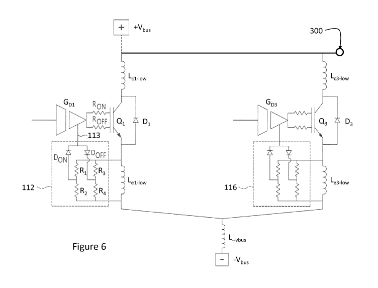
turn-on and turn-off phases. Figure 6 is a detailed view of a portion of
Figure 5
illustrating a compensation circuit according to a first illustrative
embodiment.
Figure 6 shows the bottom portion of the parallelized legs 100 and 200 with an
embodiment of the compensation circuit 112.
[0057] For concision purpose, only the compensation circuit 112 and
CA 02930188 2016-05-10
WO 2015/070344
PCT/CA2014/051065
its connection to the IGBT Q1 and its gate drive Gpi will be described in
detail
hereinbelow, it is to be understood that the compensation circuits 114, 116
and
118 are similarly constructed.
[0058] As shown on Figure 6, the compensation circuit 112 includes a
turn-on resistive divider circuit comprising resistors R1 and R2 connected in
series and across the parasitic inductance Lei_iow. A diode Dõ interconnects a
junction of the resistors R1 and R2 to a reference 113 of the gate driver Gpi.
[0059] Similarly, the compensation circuit 112 includes a turn-off
resistive divider circuit comprising resistors R3 and R4 connected in series
and
across the parasitic inductance Lei-low. A diode Doff interconnects a junction
of
the resistors R3 and R4 to the reference 113 of the gate driver Gpi.
[0060] The turn-on and turn-off resistive divider circuits allow a
separate adjustment of a level of the induced voltage that is fed back to the
gate driver Gpi. Upon turn-off of the IGBT Q1, a negative variation of the
current passing through Q1 causes a drop voltage across the parasitic
inductance (this will be best understood by reference to Figure 2, which shows
the polarity of the voltage generated on the parasitic emitter inductance at
turn-
off). The emitter voltage is lower than voltage at the reference 113. The turn-
off
diode Don is at that time non-conductive while the turn-off diode Doff becomes
conductive. The opposite is true at turn-on of the IGBT Qi.The turn-on and
turn-off diodes Don and Doff therefore ensure that the correct resistive
divider is
used at the appropriate switching phases of the IGBT Q1.
[0061] It is to be noted that the gate drivers have separate control
for
the turn-on and the turn-off of the gate of their respective power electronic
switches. Accordingly, gate resistors Ron and Roff interconnect the output of
the
gate driver Gpi and the gate of the IGBT Q1, playing the role of the gate
resistor Rg of Figures 3 and 4, at the distinct switching phases. Increasing
values of the gate resistors IR0n and Roff slows down the rate of change of
the
current at turn-on and turn-off while decreasing their values speeds up this
rate
of change at turn-on and turn-off. This is open loop action does not take into
CA 02930188 2016-05-10
WO 2015/070344
PCT/CA2014/051065
16
account the differences in parasitic inductances of the power circuit that has
a
great impact on the commutation.
[0062] Accordingly, for the turn-off, the ratio of R3 over R4
combined
with Roff sets the rate of current fall in the IGBT Q1. The values of the two
gate
resistors R3 and R4 determine the feedback portion of the voltage sampled
across the parasitic emitter inductance that is injected in the gate circuit
of the
IGBT Q1. Values of gate resistors are adjusted to control the turn-off loss,
thereby controlling the thermal stress on the IGBT Q1 and keeping the
overvoltage on the IGBT Q1 below its maximum rating.
[0063] For the turn-on, the ratio of R1 over R2 combined with Rõ sets
the current rise rate the IGBT Q1. The values of the gate two resistors R1 and
R2, determine the feedback portion of the voltage sampled across the parasitic
emitter inductance that is injected in the gate circuit of the IGBT Q1. Values
of
these resistors and of the corresponding resistors of the compensation circuit
116 are adjusted to balance the turn-on losses between the parallelized IGBTs
Qi and Q3, controlling their thermal stress while also maintaining the
recovery
current of the opposite freewheel diodes within their maximum ratings.
[0064] The present technology separately adjusts, by a closing loop
action, the rates of current rise and fall times of each IGBT placed in
parallel
with another IGBT (or more generally between each power electronic switch
placed in parallel with another power electronic switch) according to
parasitic
inductances of their respective legs. It therefore allows balancing their
switching losses while also controlling their overvoltage at turn-off as well
as
the recovery current at turn-on. This technology equalizes stresses applied to
the power electronic switches.
[0065] Figure 7 is a detailed view of a portion of Figure 5
illustrating a
compensation circuit according to a second illustrative embodiment. The
second embodiment of Figure 7 discloses a compensation circuit 122 that
differs from the compensation circuit 112 in that the resistor R2 and the turn-
off
diode Doff have been removed.
CA 02930188 2016-05-10
WO 2015/070344
PCT/CA2014/051065
17
[0066] The compensation circuit 122 thus includes the resistor R1 that
is so connected as to be parallel with resistor R3 during turn-on, when the
emitter voltage of the IGBT Q1 is higher than the reference 113. The diode Dõ
interconnects the resistor R1 to the reference 113 of the gate driver Gpi.
Accordingly, the values of R1 in parallel with R3 and the value of R4 are
selected to feed back the adequate portion of signal to the gate driver during
turn-on.
[0067] The compensation circuit 122 forms a turn-off resistive divider
circuit comprising resistors R3 and R4 connected in series and across the
parasitic emitter inductance Lel-low. The diode Doff is not required in the
configuration of the compensation circuit 122 since the configuration of the
diode Don ensures that the resistor R1 is not in play at turn-off.
[0068] During turn-off, a ratio of R3 over R4 combined with Roff sets
the current fall rate to adjust the overvoltage limit in the IGBT Q1. Values
of the
two resistors R3 and R4 determine the feedback portion of the voltage induced
in the parasitic emitter inductance that is injected in the gate circuit of
the IGBT
Qi. The values of these resistors are adjusted to keep the overvoltage on the
IGBT Q1 under its rated limit and to balance turn-off losses between the IGBTs
Q/ and Q3, the latter benefiting from the use of a similar compensation
circuit
124.
[0069] It may be noted that while the compensation circuit 122 has
less elements than the compensation circuit 112 of Figure 6, the resistor R2
and the diode Doff being absent, this compensation circuit provides less
adjustment flexibility.
[0070] In the foregoing, the voltage induced across the parasitic
emitter inductance Lei-low was selected to be fed back to the gate driver Gpi
to
improve the behavior of the IGBT Q1 at turn-on and turn-off and to reduce the
dynamic unbalance that may occur in the case of parallelized power electronic
switches by balancing their switching currents at turn-on and turn-off.
Alternatively, voltages induced in other parasitic inductances may also be
used
CA 02930188 2016-05-10
WO 2015/070344
PCT/CA2014/051065
18
to provide such feedback, inasmuch as the sample voltage is obtained from a
parasitic inductance of the same leg as the power electronic switch that is
being controlled.
[0071] The present description of the compensation circuits 112 and
122, which also applies to the other compensation circuits, have been shown
and described referring to resistive circuits used to select the portion of
the
voltage induced in the parasitic emitter inductances. Use of other types of
circuits to select a portion of the induced voltage, such as for example
circuits
including transformers or other voltage adaptors, is also contemplated.
[0072] The foregoing describes solutions applicable to DC-DC
converters and to DC-AC power converters, for example to commutation cells
using a full leg of semiconductors, opposite pairs of power electronic
switches
and freewheel diodes or to parallel semiconductor legs, to provide alternative
current to a connected load such as a motor of an electric vehicle.
[0073] Those of ordinary skill in the art will realize that the
description
of the commutation cell, power converter and compensation circuit are
illustrative only and are not intended to be in any way limiting. Other
embodiments will readily suggest themselves to such persons with ordinary
skill in the art having the benefit of the present disclosure. Furthermore,
the
commutation cell, power converter and compensation circuit may be
customized to offer valuable solutions to existing needs and problems related
to variable characteristics of power electronic switches used in commutation
cells and in power converters.
[0074] In the interest of clarity, not all of the routine features of
the
implementations of the commutation cell, power converter and compensation
circuit are shown and described herein. It will, of course, be appreciated
that in
the development of any such actual implementation of the commutation cell,
power converter and compensation circuit, numerous implementation-specific
decisions may need to be made in order to achieve the developer's specific
goals, such as compliance with application-, system-, and business-related
CA 02930188 2016-05-10
WO 2015/070344
PCT/CA2014/051065
19
constraints, and that these specific goals will vary from one implementation
to
another and from one developer to another. Moreover, it will be appreciated
that a development effort might be complex and time-consuming, but would
nevertheless be a routine undertaking of engineering for those of ordinary
skill
in the field of power electronics having the benefit of the present
disclosure.
[0075] It is to be understood that the commutation cell, power
converter and compensation circuit are not limited in their application to the
details of construction and parts illustrated in the accompanying drawings and
described hereinabove. The proposed commutation cell, power converter and
compensation circuit are capable of other embodiments and of being practiced
in various ways. It is also to be understood that the phraseology or
terminology
used herein is for the purpose of description and not limitation. Hence,
although the commutation cell, power converter and compensation circuit have
been described hereinabove by way of illustrative embodiments thereof, they
can be modified, without departing from the spirit, scope and nature of the
subject invention.