Note: Descriptions are shown in the official language in which they were submitted.
CA 02931480 2016-05-24
WO 2015/080991 PCT/US2014/067026
SYSTEMS, METHODS, AND DEVICES HAVING STRETCHABLE INTEGRATED
CIRCUITRY FOR SENSING AND DELIVERING THERAPY
FIELD OF THE INVENTION
[0001] The present invention relates to systems, apparatuses, and methods
utilizing
expandable or stretchable integrated circuitry comprising sensor or effector
arrays on
expandable, flexible or stretchable substrates in or on sensing or treatment
devices.
BACKGROUND OF THE INVENTION
[0002] High quality medical sensing and imaging data has become important
in the
diagnoses and treatment of a variety of medical conditions include those
related to conditions
associated with the digestive system, conditions related to the
cardiocirculatory system,
injuries to the nervous system, cancer, and the like. Current sensing and
therapeutic devices
suffer from various disadvantages due to a lack of sophistication related to
the sensing,
imaging, and therapeutic functions. One of these disadvantages is that such
devices are
unable to achieve direct or conformal contact with the part of the body being
measured or
treated. The inability to achieve direct or conformal contact of such devices
is partially
attributable to the rigid nature of the devices and accompanying circuitry.
This rigidity
prevents devices from coming into conforming and/or direct contact with human
tissue,
which as is readily apparent, may change shape and size, and may be soft,
pliable, curved,
and/or irregularly shaped. Such rigidity thus compromises accuracy of
measurements and
effectiveness of treatment. Thus, devices, systems and methods that employ
flexible and/or
stretchable systems would be desirable.
[0003] Examples of categories that are amenable to such flexible and/or
stretchable
approaches include, endoscopy, vascular examination and treatment,
neurological treatment
and examination, tissue screening, cardiac ablation and mapping, conformal
external tissue
sensing and mapping among others . Controlled drug delivery as well a
controlled delivery
therapy such as ablation would also benefit from highly integrated stretchable
electronics as
will be demonstrated herein.
SUMMARY OF THE INVENTION
[0004] Stretchable and/or flexible electronics can mitigate or resolve many
of the
shortcomings described above and herein. Such techniques can be applied to the
areas above,
or to any area of physiological sensing, medical diagnostics, or treatment
that would be
improved by an integrated sensing and actuating facility. The invention
applies to both
1
CA 02931480 2016-05-24
WO 2015/080991 PCT/US2014/067026
treatment of humans and animals alike. In certain embodiments, the invention
may apply in
nonmedical areas as well.
[0005] Methods, systems, and devices are disclosed herein, which employ
stretchable/and
or flexible circuitry for improved sensing, including physiological sensing,
detection of
health-related parameters, and delivery of therapeutic measures. In
embodiments, the
circuitry is disposed on a stretchable, flexible, expandable, and/or
inflatable substrate. In
embodiments, circuitry comprises electronic devices, which may be active
devices, in
electronic communication with one another and programmed or configured to
generate output
and cause an output facility to display such output, deliver therapeutic
measures, generate
data regarding physiological parameters and/or make determinations of a health-
related
condition. Embodiments of the invention may include a storage facility in
communication
with the processing facility. The processing facility may cause at least one
of data generated
by the active devices and the output data to be stored in the storage facility
and may generate
output data related to the stored data. The processing facility may cause at
least one of data
generated by the active devices and the output data to be aggregated and may
generate output
data related to the aggregated data.
[0006] Some but not all embodiments are summarized below:
[0007] In embodiments of the invention, methods and systems include an
apparatus for
detecting and measuring aspects of a tissue of a subject's body that includes
an expandable
substrate on which is disposed stretchable circuitry configured to remain
functional upon
conforming to a surface of said tissue and including devices, which may be
sensing devices to
detect data indicative of a parameter of said tissue when said circuitry is in
conformal contact
with said tissue, and an array of imaging devices generating visual data; and
a processing
facility in electronic communication with said circuitry, receiving data
indicative of a
parameter of said tissue and visual data; and an output facility in electronic
communication
with said processing facility. The processing facility is configured to
generate and display
output data from the data indicative of a parameter of said tissue.
[0008] In embodiments of invention, methods and systems include an
apparatus for
measuring and detecting aspects of a tissue of a subject's body. The apparatus
includes a
stretchable substrate which contains circuitry configured to remain functional
upon
conforming to a surface of tissue. The circuitry contains a first array of
sensing devices that
contain contact sensors that generate data indicating that the array is in
contact with tissue
and generate data indicative of an area of the contact. The circuitry further
contains a second
2
CA 02931480 2016-05-24
WO 2015/080991 PCT/US2014/067026
array of sensing devices that detect data indicative of a parameter of the
tissue. The
apparatus also includes a processing facility that electronically communicates
with the
circuitry to receive data and activate sensing devices in the second array.
[0009] In an aspect of the invention, methods and systems include an
apparatus to deliver
therapy to a tissue. The apparatus contains a stretchable substrate that
contains circuitry that
can deliver therapy and is configured to remain functional upon conforming to
a surface of
the tissue. The apparatus contains a user interface configured to accept
commands from an
operator to activate the facility to deliver therapy and a processing facility
in electronic
communication with the circuitry and the user interface that receives a
command from the
operator and activates the facility to deliver therapy based on that command.
[0010] In an aspect of the invention, methods and systems include an
apparatus to deliver
ablative therapy to a tissue. The apparatus contains a stretchable substrate
that contains
stretchable circuitry that contains a facility to deliver ablative therapy and
an array of sensors
generating data indicative of electrical conduction of the tissue and is
configured to remain
functional upon conforming to a surface of the tissue. The apparatus contains
an output
facility that contains a user interface that is configured to accept a command
from an operator
to activate the facility to deliver ablative therapy. The apparatus contains a
processing
facility for generating and causing the output facility to display a map of
conductive
pathways in the tissue based on data indicative of electrical conduction of
the tissue. The
processing facility is in electronic communication with the circuitry and the
output facility.
[0011] In embodiments, the processing facility is further configured to
activate the
facility to deliver ablative therapy based on a command from an operator to
activate said
facility to deliver ablative therapy. In embodiments, the processing facility
is further
configured to determine areas of tissue having an abnormal property. Further
in
embodiments, the tissue is cardiac tissue and the abnormal property comprises
an arrhythmic
region of the cardiac tissue.
[0012] In embodiments, the processing facility is further configured to
suggest an area of
the tissue on which to deliver ablative therapy. Further in embodiments, the
suggestion is
based, in part, on the data indicative of electrical conduction of the tissue.
In embodiments,
the suggestion is based, in part, on the areas of tissue having an abnormal
property. Further
in embodiments, the user interface provides the suggestion to an operator. In
embodiments,
the user interface comprises a facility to select an area on the tissue in
which to deliver the
ablative therapy. In embodiments, the facility to select an area on the tissue
in which to
3
CA 02931480 2016-05-24
WO 2015/080991 PCT/US2014/067026
deliver the ablative therapy is a graphical depiction of a suggested area in
which to deliver
ablative therapy.
[0013] In an aspect of the invention, methods and systems include a device
to monitor
physiological parameters of an individual that contains a sheet-like substrate
provided with an
adhesive for attachment to the individual's body and able to conform to the
contours of the
individual's body. The substrate contains stretchable circuitry that contains
an array of
devices that contains sensing devices configured to remain functional upon the
substrate
confirming to the contours of the individual's body. The device contains a
processing facility
in communication with the sensing devices and generating output based on data
received
from the sensing devices.
[0014] In an aspect of the invention, methods and systems include a
flexible ECG
monitoring device that contains a tape-like substrate provided with an
adhesive for
attachment to the individual's body and able to conform to the contours of the
individual's
body. The substrate contains electrodes for generating data relating to an ECG
signal of an
individual's heart. The device contains a transmitter to wirelessly transmit
the data relating
to an ECG signal of an individual's heart and a remote processing unit
receiving the data
relating to an ECG signal of an individual's heart.
[0015] In another aspect of the invention, methods and systems include a
method to
ablate tissue. The method consists of placing stretchable circuitry comprising
an ablation
facility into conformal contact with the tissue and activating the ablation
facility while the
ablation facility is in conformal contact with the tissue.
[0016] In another aspect of the invention, methods and systems include a
method to
accurately ablate a tissue. The method consists of placing device containing
an array of
electrical conductance sensors and an ablation facility in conformal contact
with the tissue,
determining an abnormality in the tissue with the data from the electrical
conductance
sensors, and activating said ablation facility to ablate abnormal tissue.
[0017] In another aspect of the invention, methods and systems include a
method to
accurately ablate a tissue. The method consists of placing a device containing
an array of
electrical conductance sensors and an ablation facility in conformal contact
with the tissue,
determining an abnormality in the tissue with the data from the electrical
conductance
sensors, providing a suggestion on an area of tissue to ablate based upon the
determination of
an abnormality in the tissue, providing an interface to select an area of the
tissue to ablate,
4
CA 02931480 2016-05-24
WO 2015/080991 PCT/US2014/067026
and activating the ablation facility to ablate abnormal tissue based on an
area selected with
the interface.
[0018] These and other inventions will become apparent in the disclosure
below.
BRIEF DESCRIPTION OF THE DRAWINGS
[0019] The present invention will become more fully apparent from the
following
description and appended claims, taken in conjunction with the accompanying
figures.
Understanding that these figures merely depict exemplary embodiments of the
present
invention they are, therefore, not to be considered limiting of its scope. It
will be readily
appreciated that the components of the present invention, as generally
described and
illustrated in the figures herein, could be arranged and designed in a wide
variety of different
configurations. Nonetheless, the invention will be described and explained
with additional
specificity and detail through the use of the accompanying figures in which:
[0020] Figure lA is a schematic depiction of embodiments of the invention;
[0021] Figure 1B depicts an embodiment of the invention wherein certain
nodes on in the
circuitry are activated based on their contact with a subject tissue;
[0022] Figure 1C depicts and embodiment of the invention to graphically
represent areas
of interest on a tissue and to provide therapeutic suggestions;
[0023] Figure 2 depicts a buckled interconnection;
[0024] Figures 3A-E depict a stretchable electronics configuration with
semiconductor
islands mounted on an elastomeric substrate with stretchable interconnects;
[0025] Figure 4 depicts an extremely stretchable interconnect;
[0026] Figure 5 depicts a raised stretchable interconnect with expandable
elastomeric
substrate;
[0027] Figures 6A-F depict a method for controlled adhesion on an
elastomeric stamp;
[0028] Figures 7A-K illustrates the process of creating an image sensor via
stretch
processing;
[0029] Figure 8 is an illustration of a CMOS active pixel;
[0030] Figure 9 is an illustration of a second CMOS active pixel;
[0031] Figure 10 is an illustration of an interconnected pixel array with
one pixel per
island;
[0032] Figure 1 us an illustration of one example of an interconnected
pixel array with 4
pixels per island;
CA 02931480 2016-05-24
WO 2015/080991 PCT/US2014/067026
[0033] Figure 12 is an illustration of another example of an interconnected
pixel array
with 4 pixels per island;
[0034] Figure 13 is an illustration of another example of an interconnected
pixel array
with 4 pixels per island;
[0035] Figure 14 is an illustration of the typical architecture of a CMOS
imager;
[0036] Figures 15A-B depict an illustration of the backside illumination
concept;
[0037] Figures 16A-H outlines a method for transfer printing of "stretch
processed"
imaging arrays onto the curved surface of a BGA and the subsequent steps
required to
fabricate a BGA packaged curved image sensor;
[0038] Figures 17A and 17B outline steps in a method for fabricating curved
backside
illuminated imagers from stretch processed image sensors;
[0039] Figures 18A-18F outlines steps in a method for fabricating curved
backside
illuminated imagers from stretch processed image sensors an incorporating it
into a BGA
package;
[0040] Figure 19 outlines steps in a method for fabricating curved backside
illuminated
imagers from stretch processed image sensors an incorporating it into a BGA
package;
[0041] Figures 20A-20C outlines a method for incorporating curved backside
illuminated
imagers fabricated from stretch processed image sensors it into a BGA package;
[0042] Figures 21A-F is a summary of a process for fabricating curved
backside
illuminated imagers from stretch processed image sensors and then
incorporating them into a
BGA package;
[0043] Figures 22A-E illustrates a process of creating a backside
illuminated imager with
no color filter or micro-lens;
[0044] Figures 23A-F illustrates a second method for creating a backside
illuminated
imager with no color filter or lens;
[0045] Figures 24A-F illustrates a method for creating a planar backside
illuminated
image sensor;
[0046] Figures 25A-B illustrates a method for creating a camera module
using a curved
imaging array;
[0047] Figure 26 depicts an embodiment for a stretchable interconnect non-
planar
electronic structure;
[0048] Figure 27 depicts an embodiment for a stretchable non-planar
electronic imaging
device fabrication process using interconnected islands of semiconductor
elements;
6
CA 02931480 2016-05-24
WO 2015/080991 PCT/US2014/067026
[0049] Figure 28 depicts an embodiment for a single-pixel non-planar
electronic imaging
array with stretchable interconnects;
[0050] Figure 29 depicts an embodiment for a multiple-pixel non-planar
electronic
imaging array with stretchable interconnects;
[0051] Figure 30 depicts an embodiment for a stretchable non-planar
electronic imaging
device for replacement of a planar electronic imaging device;
[0052] Figure 31 depicts an embodiment for a stretchable non-planar
electronic imaging
structure whose surface is altered by mechanical actuation;
[0053] Figure 32 depicts an embodiment for a stretchable non-planar
electronic imaging
device fabrication process using transfer printing;
[0054] Figure 33 depicts an embodiment for a planar electronic back-side
illumination
imaging device fabrication process using transfer printing;
[0055] Figure 34A depicts an embodiment of the invention wherein
stretchable circuitry
is applied to a balloon catheter, in which the balloon catheter is deflated;
[0056] Figure 34B is an expanded view of the circuitry shown in Figure 34A;
[0057] Figure 34C depicts an embodiment of the invention wherein
stretchable circuitry
is applied to a balloon catheter, in which the balloon catheter is inflated;
[0058] Figure 35A shows a side view of a balloon with a PDMS layer wrapped
around
the surface of the balloon;
[0059] Figure 35B is a cross-sectional view which shows the catheter, the
surface of the
balloon, and the thin PDMS layer applied to the balloon;
[0060] Figure 36 depicts a process for applying stretchable circuitry to
the surface of a
catheter balloon;
[0061] Figure 37A depicts an example of a stretchable circuitry on the
surface of a
catheter balloon that is in an inflated state, wherein the interconnects in
the circuitry are
substantially coplanar with the substrate by way of the inflation;
[0062] Figure 37B depicts an example of a stretchable circuitry on the
surface of a
catheter balloon that is in a deflated state, wherein the interconnects in the
circuitry buckle
and take on compression forces imposed by deflation;
[0063] Figure 38 is an embodiment of a pressure sensor utilized with
embodiments of the
invention;
[0064] Figure 39 is a cross-sectional view of a tri-lumen catheter
according to
embodiments of the invention;
7
CA 02931480 2016-05-24
WO 2015/080991 PCT/US2014/067026
[0065] Figure 40 schematically depicts a multiplexor according to an
embodiment of the
present invention;
[0066] Figures 41A and 41B depict an embodiment of the invention where the
substrate
is furled;
[0067] Figures 42A and 42B depict the device in Figures 41A and 41B being
deployed in
the left atrium of a subject's heart;
[0068] Figures 43A and 43B depicts an embodiment of the invention being
deployed in
the left atrium of a subject's heart, wherein the substrate is inflatable;
[0069] Figure 44A shows a collapsible and expandable embodiment of the
device being
deployed in the heart of a subject.
[0070] Figure 44B depicts an example of the deployment of an epicardial
embodiment of
the device;
[0071] Figure 44C depicts another example of the deployment of an
epicardial
embodiment of the device;
[0072] Figure 44D depicts an embodiment of the invention having in
interface to show
abnormal activity and/or to suggest therapeutic activity;
[0073] Figure 45 is a schematic depiction of an embodiment of the invention
involving a
nerve prosthesis;
[0074] Figure 46 is a circuit diagram for an embodiment of the invention;
[0075] Figure 47 depicts a process for operating an array of electronic
devices according
to an embodiment of the present invention;
[0076] Figure 48 depicts an embodiment of the invention involving a nerve
prosthesis;
[0077] Figure 49 depicts an embodiment of the invention having a reservoir
for holding
and delivering a therapeutic agent, along with valves controlled by the
circuitry to deliver
said therapeutic agent;
[0078] Figure 50 depicts a process for assembling curvilinear circuitry
according to an
embodiment of the invention;
[0079] Figure 51 depicts an example of process for applying a curvilinear
array of
circuitry to an endoscopic device according to an embodiment of the invention;
[0080] Figure 52 depicts another example of a process for applying a
curvilinear array of
circuitry to an endoscopic device according to another embodiment of the
invention;
[0081] Figure 53 depicts an embodiment of an endoscopic device according to
the present
invention;
8
CA 02931480 2016-05-24
WO 2015/080991 PCT/US2014/067026
[0082]
Figure 54 depicts a tissue-screening device according to an embodiment of the
invention;
[0083]
Figure 55 is a schematic drawings of wireless RF modules that may form a part
of
an embodiment of the invention;
[0084]
Figure 56 depicts another embodiment of the invention configured for use as an
ECG monitor;
[0085]
Figure 57 shows dense arrays of conformal electrodes with metal serpentine
interconnections, according to the principles herein;
[0086]
Figures 58A¨C illustrate example endocardial applications of the apparatus and
methods, according to the principles described herein;
[0087]
Figures 59 A¨C show an example of an apparatus including strain
sensors/gauges,
according to the principles described herein; and
[0088]
Figures 60 A¨C illustrates example sensing modalities including temperature
sensors, and RF components for wireless communications, according to the
principles
described herein.
DETAILED DESCRIPTION OF THE INVENTION
[0089]
Detailed embodiments of the present invention are disclosed herein; however,
it is
to be understood that the disclosed embodiments are merely exemplary of the
invention,
which can be embodied in various forms. Therefore, specific structural and
functional details
disclosed herein are not to be interpreted as limiting but merely as a basis
for the claims and
as a representative basis for teaching one skilled in the art to variously
employ the present
invention in virtually any appropriately detailed structure. Further, the
terms and phrases
used herein are not intended to be limiting but rather to provide an
understandable description
of the invention.
[0090] The
terms "a" or "an," as used herein, are defined as one or more than one. The
term "another," as used herein, is defined as at least a second or more. The
terms "including"
and/or "having" as used herein, are defined as comprising (i.e., open
transition). The term
"coupled" or "operatively coupled," as used herein, is defined as connected,
although not
necessarily directly and not necessarily mechanically or physically.
"Electronic
communication" is the state of being able to convey or otherwise transmit data
either through
a physical connection, wireless connection, or combinations thereof.
[0091] As
described herein, the present invention comprises devices, systems, and
methods utilizing flexible and/or stretchable electronic circuits on flexible,
expandable, or
9
CA 02931480 2016-05-24
WO 2015/080991 PCT/US2014/067026
inflatable surfaces. With reference to the present invention, the term
"stretchable", and roots
and derivations thereof, when used to modify circuitry or components thereof
describes
circuitry and/or components thereof having soft or elastic properties capable
of being made
longer or wider without tearing or breaking, and it is also meant to encompass
circuitry
having components (whether or not the components themselves are individually
stretchable
as stated above) that are configured in such a way so as to accommodate a
stretchable,
inflatable, or expandable surface and remain functional when applied to a
stretchable,
inflatable, or otherwise expandable surface that is stretched, inflated, or
otherwise expanded
respectively. The term "expandable," and roots and derivations thereof, when
used to modify
circuitry or components thereof is also meant to have the meaning ascribed
above. Thus,
"stretch" and "expand," and all derivations thereof, may be used
interchangeably when
referring to the present invention. The term "flexible", and roots and
derivations thereof,
when used to modify circuitry or components thereof describes circuitry and/or
components
thereof capable of bending without breaking, and it is also meant to encompass
circuitry
having components (whether or not the components themselves are individually
flexible as
stated above) that are configured in such a way so as to accommodate a
flexible surface and
remain functional when applied to a flexible surface that is flexed or
otherwise bent. In
embodiments, at the low end of 'stretchable,' this may translate into material
strains greater
than 0.5% without fracturing, and at the high end to structures that may
stretch 100,000%
without a degradation of electrical performance. "Bendable" and roots and
derivations
thereof, when used to modify circuitry or components thereof describes
circuitry and/or
components thereof able to be shaped (at least in part) into a curve or angle,
and may
sometimes be used synonymously herein with "flexible".
[0092] Flexible, stretchable electronics address a multitude of
applications found in
nature that rigid electronics cannot. One example is a flexible neural array
to map EEG data
on the surface of the brain or of portions of cardiac tissue. Rigid
electronics cannot conform
to such surfaces.
[0093] Existing systems fail to provide implementations suitable for
environments such
as the surface of the brain or heart, particularly where such a system can
quickly assess the
relevant parameter at high spatial resolutions (e.g., through high-density
mapping).
[0094] Conformal electronics provided in various non-limiting examples
herein may be
adhered to polymeric and elastomeric surfaces (including balloons and sheets)
and may be
mechanically unfurl from the distal end of a catheter tube without causing
signal degradation.
CA 02931480 2016-05-24
WO 2015/080991 PCT/US2014/067026
The example implementations described herein facilitate multiple sensing
modalities to be
deployed in vivo in intracardial and epicardial spaces at high density
arrangements of sensing
elements. The low bending stifthess of the electronics described herein
facilitate strong
conformal contact to soft tissues (such as of the heart), without requiring
pins or separate
adhesives. Accordingly, high density mapping within the atria is afforded and
insights into
the mechanisms underlying CFAEs are allowed, including analysis of rotors and
wave fronts
in persistent AF cases. The example implementations described herein may be
used to detect
the presence of AF mechanisms at significantly reduce electrical mapping times
while
decreasing safety risks and improving clinical outcomes during ablation
procedures.
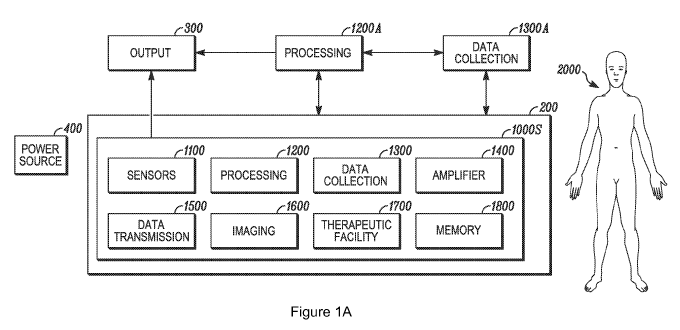
[0095] Figure lA is a schematic depiction of embodiments of the invention.
Further
description of each of the components of Figure lA will be included throughout
the
specification. Circuitry 1000S is applied, secured, or otherwise affixed to
substrate 200. In
embodiments, substrate 200 is stretchable and/or expandable as described
herein. As such
the substrate 200 can be made of a plastic material or can be made of an
elastomeric material,
or combinations thereof Note that the term "plastic" may refer to any
synthetic or naturally
occurring material or combination of materials that can be molded or shaped,
generally when
heated, and hardened into a desired shape. The term "elastomer" may refer to a
naturally
occurring material or a synthetic material, and also to a polymeric material
which can be
stretched or deformed and return to its original shape without substantial
permanent
deformation. Such elastomers may withstand substantial elastic deformations.
Examples of
elastomers used in substrate material include polymeric organosilicon
compounds
(commonly referred to as "silicones"), including Polydimethylsiloxane (PDMS).
[0096] Other materials suitable for the substrate include polyimide;
photopatternable
silicone; 5U8 polymer; PDS polydustrene; parylene and its derivatives and
copolymers
(parylene-N); ultrahigh molecular weight polyethylene; poly ether ether
ketones (PEEK);
polyurethanes (PTG Elasthane0, Dow Pellethane0); polylactic acid; polyglycolic
acid;
polymer composites (PTG Purisil Al , PTG Bionate0, PTG Carbosi10);
silicones/siloxanes
(RTV 6150, Sylgard 1840); polytetrafluoroethylene (PTFE, Teflon 0); polyamic
acid;
polymethyl acrylate; stainless steel; titanium and its alloys; platinum and
its alloys; and gold.
In embodiments, the substrate is made of a stretchable or flexible
biocompatible material
having properties which may allow for certain devices to be left in a living
organism (referred
to as the human body 2000) for a period of time without having to be
retrieved. It should be
11
CA 02931480 2016-05-24
WO 2015/080991 PCT/US2014/067026
noted that the invention applies to other living organisms, particularly
mammals and should
not be understood to be limited to humans.
[0097]
Some of the materials mentioned above, specifically parylene and its
derivatives
and copolymers (parylene-N); ultrahigh molecular weight polyethylene; poly
ether ether
ketones (PEEK); polyurethanes (PTG Elasthane0, Dow Pellethane0); polylactic
acid;
polyglycolic acid; polymer composites (PTG Purisil Al , PTG Bionate0, PTG
Carbosil);
silicones/siloxanes (RTV 6150, Sylgard 1840); polytetrafluoroethylene (PTFE,
Teflon 0);
polyamic acid; polymethyl acrylate; stainless steel; titanium and its alloys;
platinum and its
alloys; and gold, are biocompatible.
Coatings for the substrate to increase its
biocompatibility may include, PTFE, polylactic acid, polyglycolic acid, and
poly(lactic-co-
glycolic acid).
[0098] The
materials disclosed for substrate 200 herein may be understood to apply to
any of the embodiments disclosed herein that require substrate. It should also
be noted that
materials can be chosen based on their properties which include degree of
stiffness, degree of
flexibility, degree of elasticity, or such properties related to the
material's elastic moduli
including Young's modulus, tensile modulus, bulk modulus, shear modulus, etc.,
and or their
biodegradability.
[0099] The
substrate 200 can be one of any possible number of shapes or configurations.
In embodiments, the substrate 200 is substantially flat and in some
embodiments configured
to be a sheet or strip. Yet it should be noted that such flat configurations
of substrate 200
could be any number of geometric shapes. Other embodiments of flat substrates
will be
described below including substrates having a tape-like or sheet
configuration. Flexible
and/or stretchable substrate 200 having a sheet or otherwise substantially
flat configuration
may be configured such that substrate 200 can be folded, furled, bunched,
wrapped or
otherwise contained. In embodiments, a substrate 200 configured as such can be
folded,
furled, bunched, collapsed (such as in an umbrella-like configuration),
wrapped, or otherwise
contained during delivery through narrow passageways in the subject's body
2000 and then
deployed into an unfolded, unfurled, un-collapsed, etc. state once in position
for deployment.
As a non-limiting example, a furled substrate 200 carrying circuitry 100S
comprising sensing
device 1100 could be delivered via a catheter, then unfurled at such point
when it is desired
for the sensing device to contact the tissue of interest, such as the surface
of the heart (inner
or outer), or the inner surface of a lumen such as the pulmonary vein. In
embodiments,
substrates 200 may also be formed into concave and convex shapes, such as
lenses. Such
12
CA 02931480 2016-05-24
WO 2015/080991 PCT/US2014/067026
convex and concave substrates can be made of material suitable for contact
with the eye, such
as a contact lens, or for implantation into the eye, such a retinal or corneal
implant.
[00100] Substrate 200 may also be three-dimensional. The three-dimensional
substrate
200 can be any number of shapes. Such three-dimensional substrates may be a
solid or
substantially solid. In embodiments, the three-dimensional substrate may be
pliable, flexible
and stretchable while still comprising homogeneous or substantially homogenous
material
throughout its form, such as a foam or a flexible/stretchable polymeric
sphere, ovoid,
cylinder, disc, or other three-dimensional object. In embodiments, the three-
dimensional
substrate 200 may be made from several materials. In the presently preferred
embodiment
for the three-dimensional substrate 200, the substrate is an inflatable body
(also referred to
herein as an elastomeric vessel). Inflatable bodies of this type may be
stretchable, such as a
balloon or the like; however, in other embodiments, the inflatable body
inflates without
stretching. In embodiments, inflation can be achieved via a gas or liquid. In
certain
embodiments, inflation with a viscous fluid is preferable, but it should be
clear that a variety
of gases, fluids or gels may be employed for such inflation. Embodiments
comprising
balloon-like and disc-like inflatable substrates will be discussed in further
detail below. The
systems to achieve inflation discussed in connection with those embodiments
apply to all
inflatable embodiments of substrate herein.
[00101] In embodiments where the substrate 200 is stretchable, circuitry 1000S
is
configured in the applicable manners described herein to be stretchable and/or
to
accommodate such stretching of the substrate 200. Similarly, in embodiments
where the
substrate 200 is flexible, but not necessarily stretchable, circuitry 1000S is
configured in the
applicable manners described herein to be flexible and/or accommodate such
flexing of the
substrate 200. Circuitry 1000S can be applied and/or configured using
applicable techniques
described below, including those described in connection with exemplary
embodiments.
[00102] As mentioned above, the present invention may employ one or more of a
plurality
of flexible and/or stretchable electronics technologies in the implementation
thereof.
Traditionally, electronics have been fabricated on rigid structures, such as
on integrated
circuits, hybrid integrated circuits, flexible printed circuit boards, and on
printed circuit
boards. Integrated circuits, also referred to as ICs, microcircuits,
microchips, silicon chips, or
simple chips, have been traditionally fabricated on a thin substrate of
semiconductor material,
and have been constrained to rigid substrates mainly due to the high
temperatures required in
the step of inorganic semiconductor deposition. Hybrid integrated circuits and
printed circuit
13
CA 02931480 2016-05-24
WO 2015/080991 PCT/US2014/067026
boards have been the main method for integrating multiple ICs together, such
as through
mounting the ICs onto a ceramic, epoxy resin, or other rigid non-conducting
surface. These
interconnecting surfaces have traditionally been rigid in order to ensure that
the electrical
interconnection methods, such as solder joints to the board and metal traces
across the boards,
do not break or fracture when flexed. In addition, the ICs themselves may
fracture if flexed.
Thus, the field of electronics has been largely constrained to rigid
electronics structures,
which then tend to constrain electronics applications that may require
flexibility and or
stretchability necessary for the embodiments disclosed herein.
[00103] Advancements in flexible and bendable electronics technologies have
emerged
that enable flexible electronics applications, such as with organic and
inorganic
semiconductors on flexible plastic substrates, and other technologies
described herein.
Further, stretchable electronics technologies have emerged that enable
applications that
require the electronics to be stretchable, such as through the use of mounting
ICs on flexible
substrates and interconnected through some method of stretchable electrical
interconnect, and
other technologies as described herein. The present invention may utilize one
or more of
these flexible, bendable, stretchable, and like technologies, in applications
that require the
electronics to operate in configurations that may not be, or remain, rigid and
planar, such as
applications that require electronics to flex, bend, expand, stretch and the
like.
[00104] In embodiments, the circuitry of the invention may be made in part or
in full by
utilizing the techniques and processes described below. Note that the below
description of
the various ways to achieve stretchable and/or flexible electronics is not
meant to be limiting,
and encompasses suitable variants and or modifications within the ambit of one
skilled in the
art. As such, this application will refer to the following United States
Patents and Patent
Applications, each of which is incorporated by reference herein in its
entirety: United States
Patent No. 7,557,367 entitled "Stretchable Semiconductor Elements and
Stretchable
Electrical Circuits", issued July 7, 2009 (the '367 patent"); United States
Patent No.
7,521,292 entitled "Stretchable Form of Single Crystal Silicon for High
Performance
Electronics on Rubber Substrates", issued April 29, 2009 (the '292 patent");
United States
Published Patent Application No. 20080157235 entitled "Controlled Buckling
Structures in
Semiconductor Interconnects and Nano membranes for Stretchable Electronics",
filed
September 6, 2007 (the '235 application"); United States Patent Application
having Serial
No. 12/398,811 entitled "Stretchable and Foldable Electronics", filed March 5,
2009 (the
'811 application"); United States Published Patent Application No. 20040192082
entitled
14
CA 02931480 2016-05-24
WO 2015/080991 PCT/US2014/067026
"Stretchable and Elastic Interconnects" filed March 28, 2003(the '082
application"); United
States Published Patent Application No. 20070134849 entitled "Method For
Embedding
Dies", filed November 21, 2006 (the '849 application"); United States
Published Patent
Application No. 20080064125 entitled "Extendable Connector and Network, filed
September
12, 2007 (the "125 application"); United States Provisional Patent Application
having Serial
No. 61/240,262 (the '262 application") "Stretchable Electronics", filed
September 7, 2009;
United States Patent Application having Serial No. 12/616,922 entitled
"Extremely
Stretchable Electronics", filed November 12, 2009 (the '922 application");
United States
Provisional Patent Application having Serial No. 61/120,904 entitled "Transfer
Printing",
filed December 9, 2008 (the '904 application"); United States Published Patent
Application
No. 20060286488 entitled "Methods and Devices for Fabricating Three-
Dimensional
Nanoscale Structures", filed December 1, 2004; United States Patent No.
7,195,733 entitled
"Composite Patterning Devices for Soft Lithography" issued March 27, 2007;
United States
Published Patent Application No. 20090199960 entitled "Pattern Transfer
Printing by Kinetic
Control of Adhesion to an Elastomeric Stamp" filed June 9, 2006; United States
Published
Patent Application. No. 20070032089 entitled "Printable Semiconductor
Structures and
Related Methods of Making and Assembling" filed June 1, 2006; United States
Published
Patent Application No. 20080108171 entitled "Release Strategies for Making
Transferable
Semiconductor Structures, Devices and Device Components" filed September 20,
2007; and
United States Published Patent Application No. 20080055581 entitled "Devices
and Methods
for Pattern Generation by Ink Lithography", filed February 16, 2007.
[00105] "Electronic device" a/k/a "device" is used broadly herein to encompass
an
integrated circuit(s) having a wide range of functionality. In embodiments,
the electronic
devices may be devices laid out in a device island arrangement, as described
herein including
in connection to exemplary embodiments. The devices can be, or their
functionality can
include, integrated circuits, processors, controllers, microprocessors,
diodes, capacitors,
power storage elements, antennae, ASICs, sensors, image elements (e.g. CMOS,
CCD
imaging elements), amplifiers, AID and D/A converters, associated differential
amplifiers,
buffers, microprocessors, optical collectors, transducer including electro-
mechanical
transducers, piezo-electric actuators, light emitting electronics which
include LEDs, logic,
memory, clock, and transistors including active matrix switching transistors,
and
combinations thereof. The purpose and advantage of using standard ICs (in
embodiments,
CMOS, on single crystal silicon) is to have and use high quality, high
performance, and high
CA 02931480 2016-05-24
WO 2015/080991 PCT/US2014/067026
functioning circuit components that are also already commonly mass-produced
with well
known processes, and which provide a range of functionality and generation of
data far
superior to that produced by a passive means. Components within electronic
devices or
devices are described herein, and include those components described above. A
component
can be one or more of any of the electronic devices described above and/or may
include a
photodiode, LED, TUFT, electrode, semiconductor, other light-
collecting/detecting
components, transistor, contact pad capable of contacting a device component,
thin-film
devices, circuit elements, control elements, microprocessors, interconnects,
contact pads,
capacitors, resistors, inductors, memory element, power storage element,
antenna, logic
element, buffer and/or other passive or active components. A device component
may be
connected to one or more contact pads as known in the art, such as metal
evaporation, wire
bonding, application of solids or conductive pastes, and the like.
[00106] Components incapable of controlling current by means of another
electrical signal
are called passive devices. Resistors, capacitors, inductors, transformers,
and diodes are all
considered passive devices
[00107] For purposes of the invention, an active device is any type of circuit
component
with the ability to electrically control electron flow. Active devices
include, but are not
limited to, vacuum tubes, transistors, amplifiers, logic gates, integrated
circuits,
semiconducting sensors and image elements, silicon-controlled rectifiers
(SCRs), and triode
for alternating current (TRIACs).
[00108] "Ultrathin" refers to devices of thin geometries that exhibit
flexibility.
[00109] "Functional layer" refers to a device layer that imparts some
functionality to the
device. For example, the functional layer may be a thin film, such as a
semiconductor layer.
Alternatively, the functional layer may comprise multiple layers, such as
multiple
semiconductor layers separated by support layers. The functional layer may
comprise a
plurality of patterned elements, such as interconnects running between device-
receiving pads.
[00110] Semiconductor materials which may be used to make circuits may include
amorphous silicon, polycrystalline silicon, single crystal silicon, conductive
oxides, carbon
annotates and organic materials.
[00111] In some embodiments of the invention, semiconductors are printed onto
flexible
plastic substrates, creating bendable macro-electronic, micro-electronic,
and/or nano-
electronic devices. Such bendable thin film electronics devices on plastic may
exhibit field
effect performance similar to or exceeding that of thin film electronics
devices fabricated by
16
CA 02931480 2016-05-24
WO 2015/080991 PCT/US2014/067026
conventional high temperature processing methods. In addition, these flexible
semiconductor
on plastic structures may provide bendable electronic devices compatible with
efficient high
throughput processing on large areas of flexible substrates at lower
temperatures, such as
room temperature processing on plastic substrates. This technology may provide
dry transfer
contact printing techniques that are capable of assembling bendable thin film
electronics
devices by depositing a range of high quality semiconductors, including single
crystal Si
ribbons, GaAs, INP wires, and carbon nano-tubes onto plastic substrates. This
high
performance printed circuitry on flexible substrates enables an electronics
structure that has
wide ranging applications. The '367 patent and associated disclosure
illustrates an example
set of steps for fabricating a bendable thin film electronics device in this
manner. (See Fig.
26A of the '367 patent for Example).
[00112] In addition to being able to fabricate semiconductor structures on
plastic, it has
been demonstrated that metal-semiconductor electronics devices may be formed
with
printable wire arrays, such as GaAs micro-wires, on the plastic substrate.
Similarly, other
high quality semiconductor materials have been shown to transfer onto plastic
substrates,
including Si nano-wires, micro-ribbons, platelets, and the like. In addition,
transfer-printing
techniques using elastomeric stamps may be employed. The '367 patent provides
an example
illustration of the major steps for fabricating, on flexible plastic
substrates, electronics
devices that use arrays of single wires (in this instance GaAs wires) with
epitaxial channel
layers, and integrated holmic contacts. (See Figure 41 of the '367 patent). In
an example, a
semi-insulating GaAs wafer may provide the source material for generating the
micro-wires.
Each wire may have multiple ohmic stripes separated by a gap that defines the
channel length
of the resultant electronic device. Contacting a flat, elastomeric stamp of
PDMS to the wires
forms a van der Waals bond. This interaction enables removal of all the wires
from the wafer
to the surface of the PDMS when the stamp is peeled back. The PDMS stamp with
the wires
is then placed against an uncured plastic sheet. After curing, peeling off the
PDMS stamp
leaves the wires with exposed ohmic stripes embedded on the surface of the
plastic substrate.
Further processing on the plastic substrate may define electrodes that connect
the ohmic
stripes to form the source, drain, and gate electrodes of the electronics
devices. The resultant
arrays are mechanically flexible due to the bendability of the plastic
substrate and the wires.
[00113] In embodiments, and in general, stretchable electronics may
incorporate
electrodes, such as connected to a multiplexing chip and data acquisition
system. In an
example, an electrode may be fabricated, designed, transferred, and optionally
encapsulated.
17
CA 02931480 2016-05-24
WO 2015/080991 PCT/US2014/067026
In an embodiment, the fabrication may utilize and/or include an SI wafer; spin
coating an
adhesion layer (e.g. an HMDS adhesion layer); spin coating (e.g. PMMA)
patterned by
shadow mask, such as in oxygen RIE; spin coating Polyimide; depositing PECVD
5i02; spin
1813 Resist, photolithography patterning; metal evaporation (e.g. Ti, Pt, Au,
and the like, or
combination of the aforementioned); gold etchant, liftoff in hot acetone; spin
Polyimide;
PECVD 5i02; spin 1813 Resist, photolithography patterning; RIE etch, and the
like. In this
embodiment, the fabrication step may be complete with the electrodes on the Si
wafer. In
embodiments, the Si wafer may then be bathed in a hot acetone bath, such as at
100C for
approximately one hour to release the adhesion layer while PI posts keep
electrode adhered to
the surface of the Si wafer. In embodiments, electrodes may be designed in a
plurality of
shapes and distributed in a plurality of distribution patterns. Electrodes
may be
interconnected to electronics, multiplexing electronics, interface
electronics, a
communications facility, interface connections, and the like including any of
the
facilities/elements described on connection with Figure lA and/or the
exemplary
embodiments herein. In embodiments, the electrodes may be transferred from the
Si wafer to
a transfer stamp, such as a PDMS stamp, where the material of the transfer
stamp may be
fully cured, partially cured, and the like. For example, a partially cured
PDMS sheet may be
¨350nm, where the PDMS was spun on at 300 rpm for 60s, cured 65C for 25 min,
and used
to lift electrodes off of the PDMS sheet. In addition, the electrodes may be
encapsulated,
such as wherein the electrodes are sandwiched between a supporting PDMS layer
and second
PDMS layer while at least one of the PDMS layers is partially cured.
[00114] In embodiments, stretchable electronics configurations may incorporate
flex PCB
design elements, such as flex print, chip-flip configurations (such as bonded
onto the PCB),
and the like, for connections to electrodes and/or devices, and for
connections to interface
electronics, such as to a data acquisition system (DAQ). For example, a flex
PCB may be
joined to electrodes by an anisotropic conductive film (ACF) connection,
solder joints may
connect flex PCB to the data acquisition system via conductive wires, and the
like. In
embodiments, the electrodes may be connected onto a surface by employing a
partially cured
elastomer (e.g. PDMS) as an adhesive.
[00115] In embodiments, stretchable electronics may be formed into sheets of
stretchable
electronics. In embodiments, stretchable sheets may be thin, such as
approximately 100 lam.
Optionally, amplification and multiplexing may be implemented without
substantially heating
the contact area, such as with micro-fluidic cooling.
18
CA 02931480 2016-05-24
WO 2015/080991 PCT/US2014/067026
[00116] In embodiments, a sheet having arrays of electronic devices comprising
electrodes
may be cut into different shapes and remain functional, such as through
communicating
electrode islands which determine the shape of the electrode sheet. Electrodes
are laid out in
a device island arrangement (as described herein) and may contain active
circuitry designed
to communicate with each other via inter-island stretchable interconnects so
that processing
facility (described herein) in the circuitry can determine in real-time the
identity and location
of other such islands. In this way, if one island becomes defective, the
islands can still send
out coordinated, multiplexed data from the remaining array. Such functionality
allows for
such arrays to be cut and shaped based on the size constraints of the
application. A sheet, and
thus circuitry, may be cut to side and the circuitry will poll remaining
electrodes and/or
devices to determine which are left and will modify the calibration
accordingly. An example
of a stretchable electronics sheet containing this functionality, may include
electrode
geometry, such as a 20x20 array of platinum electrodes on lmm pitch for a
total area of
20x20 mm2; an electrode impedance, such as 5kohm at lkhz (adjustable); a
configuration in a
flexible sheet, such as with a 50 [an total thickness, and polyimide
encapsulated; a sampling
rate, such as 2 kHz per channel; a voltage dynamic range, such as +/- 6 mV; a
dc voltage
offset range, such as -2.5 to 5 V, with dc rejection; a voltage noise, such as
0.002 mV, a
maximum signal-to-noise ratio, such as 3000; a leakage current, such as 0.3
[LA typical, 10
[LA maximum, as meets IEC standards, and the like; an operating voltage of 5
V; an operating
power per channel, such as less than 2 mW (adjustable); a number of interface
wires, such as
for power, ground, low impedance ground, data lines, and the like; a voltage
gain, such as
150; a mechanical bend radius, such as 1 mm; a local heating capability, such
as heating local
tissue by up to 1 C; biocompatibility duration, such as 2 weeks; active
electronics, such as a
differential amplifier, a multiplexer (e.g. 1000 transistors per channel); a
data acquisition
system, such as with a 16 bit AID converter with a 500kHz sampling rate, less
than 2 [LV
noise, data login and real-time screen display; safety compliance, such as to
IEC10601; and
the like.
[00117] In embodiments of the invention, mechanical flexibility may represent
an
important characteristic of devices, such as on plastic substrates, for many
applications.
Micro/nano-wires with integrated ohmic contacts provide a unique type of
material for high
performance devices that can be built directly on a wide range of device
substrates.
Alternatively, other materials may be used to connect electrical components
together, such as
19
CA 02931480 2016-05-24
WO 2015/080991 PCT/US2014/067026
connecting electrically and/or mechanically by thin polymer bridges with or
without metal
interconnects lines.
[00118] In embodiments, an encapsulation layer may be utilized. An
encapsulating layer
may refer to coating of the device, or a portion of the device. In
embodiments, the
encapsulation layer may have a modulus that is inhomogeneous and/or that
spatially varies.
Encapsulation layers may provide mechanical protection, device isolation, and
the like.
These layers may have a significant benefit to stretchable electronics. For
example, low
modulus PDMS structures may increase the range of stretchability significantly
(described at
length in the '811 application). The encapsulation layer may also be used as a
passivation
later on top of devices for the protection or electrical isolation. In
embodiments, the use of
low modulus strain isolation layers may allow integration of high performance
electronics.
The devices may have an encapsulation layer to provide mechanical protection
and protection
against the environment. The use of encapsulation layers may have a
significant impact at
high strain. Encapsulants with low moduli may provide the greatest flexibility
and therefore
the greatest levels of stretchability. As referred to in the '811 application,
low modulus
formulations of PDMS may increase the range of stretchability at least from
60%.
Encapsulation layers may also relieve strains and stresses on the electronic
device, such as on
a functional layer of the device that is vulnerable to strain induced failure.
In embodiments, a
layering of materials with different moduli may be used. In embodiments, these
layers may
be a polymer, an elastomer, and the like. In embodiments, an encapsulation may
serve to
create a biocompatible interface for an implanted stretchable electronic
system, such as Silk
encapsulation of electronic devices in contact with tissue.
[00119] Returning to flexible and stretchable electronics technologies that
may be utilized
in the present invention, it has been shown that buckled and wavy ribbons of
semiconductor,
such as GaAs or Silicon, may be fabricated as part of electronics on
elastomeric substrates.
Semiconductor ribbons, such as with thicknesses in the submicron range and
well-defined,
'wavy' and/or 'buckled' geometries have been demonstrated. The resulting
structures, on the
surface of, or embedded in, the elastomeric substrate, have been shown to
exhibit reversible
stretchability and compressibility to strains greater than 10%. By integrating
ohmic contacts
on these structured GaAs ribbons, high-performance stretchable electronic
devices may be
achieved. The '292 patent illustrates steps for fabricating stretchable GaAs
ribbons on an
elastomeric substrate made of PDMS, where the ribbons are generated from a
high-quality
bulk wafer of GaAs with multiple epitaxial layers (See Fig. 22 in the '292
patent). The wafer
CA 02931480 2016-05-24
WO 2015/080991 PCT/US2014/067026
with released GaAs ribbons is contacted to the surface of a pre-stretched
PDMS, with the
ribbons aligned along the direction of stretching. Peeling the PDMS from the
mother wafer
transfers all the ribbons to the surface of the PDMS. Relaxing the prestrain
in the PDMS
leads to the formation of large-scale buckles/wavy structures along the
ribbons. The
geometry of the ribbons may depend on the prestrain applied to the stamp, the
interaction
between the PDMS and ribbons, and the flexural rigidity of the ribbons, and
the like. In
embodiments, buckles and waves may be included in a single ribbon along its
length, due for
example, to thickness variations associated with device structures. In
practical applications,
it might be useful to encapsulate the ribbons and devices in a way that
maintains their
stretchability. The semiconductor ribbons on an elastomeric substrate may be
used to
fabricate high-performance electronic devices, buckled and wavy ribbons of
semiconductor
multilayer stacks and devices exhibiting significant
compressibility/stretchability. In
embodiments, the present invention may utilize a fabrication process for
producing an array
of devices utilizing semiconductor ribbons, such as an array of CMOS inverters
with
stretchable, wavy interconnects. Also, a strategy of top layer encapsulation
may be used to
isolate circuitry from strain, thereby avoiding cracking.
[00120] In embodiments, a neutral mechanical plane (NMP) in a multilayer stack
may
define the position where the strains are zero. For instance, the different
layers may include a
support layer, a functional layer, a neutral mechanical surface adjusting
layer, an
encapsulation layer with a resultant neutral mechanical surface such as
coincident with the
functional layer, and the like. In embodiments, the functional layer may
include flexible or
elastic device regions and rigid island regions. In embodiments, an NMP may be
realized in
any application of the stretchable electronics as utilized in the present
invention.
[00121] In embodiments, semiconductor ribbons (also, micro-ribbons, nano-
ribbons, and
the like) may be used to implement integrated circuitry, electrical
interconnectivity between
electrical/electronic components, and even for mechanical support as a part of
an electrical
/electronic system. As such, semiconductor ribbons may be utilized in a great
variety of
ways in the configuration /fabrication of flexible and stretchable
electronics, such as being
used for the electronics or interconnection portion of an assembly leading to
a flexible and/or
stretchable electronics, as an interconnected array of ribbons forming a
flexible and/or
stretchable electronics on a flexible substrate, and the like. For example,
nano-ribbons may
be used to form a flexible array of electronics on a plastic substrate. The
array may represent
an array of electrode-electronics cells, where the nano-ribbons are pre-
fabricated, and then
21
CA 02931480 2016-05-24
WO 2015/080991 PCT/US2014/067026
laid down and interconnected through metallization and encapsulation layers.
Note that the
final structure of this configuration may be similar to electronic device
arrays as fabricated
directly on the plastic, as described herein, but with the higher electronics
integration density
enabled with the semiconductor ribbons. In addition, this configuration may
include
encapsulation layers and fabrication steps which may isolate the structure
from a wet
environment. This example is not meant to limit the use of semiconductor
ribbons in any
way, as they may be used in a great variety of applications associated with
flexibility and
stretchability. For example, the cells of this array may be instead connected
by wires, bent
interconnections, be mounted on an elastomeric substrate, and the like, in
order to improve
the flexibility and/or stretchability of the circuitry.
[00122] Wavy semiconductor interconnects is only one form of a broader class
of flexible
and stretchable interconnects that may (in some cases) be referred to as
'bent' interconnects,
where the material may be semiconductor, metal, or other conductive material,
formed in
ribbons, bands, wire, traces, and the like. A bent configuration may refer to
a structure
having a curved shape resulting from the application of a force, such as
having one or more
folded regions. These bent interconnections may be formed in a variety of
ways, and in
embodiments, where the interconnect material is placed on an elastomeric
substrate that has
been pre-strained, and the bend form created when the strain is released. In
embodiments, the
pre-strain may be pre-stretched or pre-compressed, provided in one, two, or
three axes,
provided homogeneously or heterogeneously, and the like. The wavy patterns may
be
formed along pre-strained wavy patterns, may form as 'pop-up' bridges, may be
used with
other electrical components mounted on the elastomer, or transfer printed to
another
structure. Alternately, instead of generating a 'pop-up' or buckled components
via force or
strain application to an elastomeric substrate, a stretchable and bendable
interconnect may be
made by application of a component material to a receiving surface. Bent
configurations may
be constructed from micro-wires, such as transferred onto a substrate, or by
fabricating wavy
interconnect patterns either in conjunction with electronics components, such
as on an
elastomeric substrate.
[00123] Semiconductor nanoribbons, as described herein, may utilize the method
of
forming wavy 'bent' interconnections through the use of forming the bent
interconnection on
a pre-strained elastomeric substrate, and this technique may be applied to a
plurality of
different materials. Another general class of wavy interconnects may utilize
controlled
buckling of the interconnection material. In this case, a bonding material may
be applied in a
22
CA 02931480 2016-05-24
WO 2015/080991 PCT/US2014/067026
selected pattern so that there are bonded regions that will remain in physical
contact with the
substrate (after deformation) and other regions that will not. The pre-
strained substrate is
removed from the wafer substrate, and upon relaxation of the substrate, the
unbounded
interconnects buckle (pop-up') in the unbonded (or weakly bonded) regions.
Accordingly,
buckled interconnects impart stretchability to the structure without breaking
electrical contact
between components, thereby providing flexibility and/or stretchability.
Figure 2 shows a
simplified diagram showing a buckled interconnection 204S between two
components 202S
and 208S.
[00124] In embodiments, any, all, or combinations of each of the
interconnection schemes
described herein may be applied to make an electronics support structure more
flexible or
bendable, such as applying bent interconnects to a flexible substrate, such as
plastic or
elastomeric substrates. However, these bent interconnect structures may
provide for a
substantially more expandable or stretchable configuration in another general
class of
stretchable electronic structures, where rigid semiconductor islands are
mounted on an
elastomeric substrate and interconnected with one of the plurality of bent
interconnect
technologies. This technology is presented here, and also in the '262
application, which has
been incorporated by reference in its entirety. This configuration also uses
the neutral
mechanical plane designs, as described herein, to reduce the strain on rigid
components
encapsulated within the system. These component devices may be thinned to the
thickness
corresponding to the desired application or they may be incorporated exactly
as they are
obtained. Devices may then be interconnected electronically and encapsulated
to protect
them from the environment and enhance flexibility and stretchability.
[00125] In an embodiment, the first step in a process to create stretchable
and flexible
electronics as described herein involves obtaining required electronic devices
and
components and conductive materials for the functional layer. The electronics
are then
thinned (if necessary) by using a back grinding process. Many processes are
available that
can reliably take wafers down to 50 microns. Dicing chips via plasma etching
before the
grinding process allows further reduction in thickness and can deliver chips
down to 20
microns in thickness. For thinning, typically a specialized tape is placed
over the processed
part of the chip. The bottom of the chip is then thinned using both mechanical
and/or
chemical means. After thinning, the chips may be transferred to a receiving
substrate,
wherein the receiving substrate may be a flat surface on which stretchable
interconnects can
be fabricated. Figure 3 illustrates an example process, which begins by
creating a flexible
23
CA 02931480 2016-05-24
WO 2015/080991 PCT/US2014/067026
substrate 302S on the carrier 308S coated with a sacrificial layer 304S
(Figure 3A), placing
devices 310S on the flexible substrate (Figure 3B), and performing a
planarization step in
order to make the top surface of the receiving substrate the same height as
that of the die
surface (Figure 3C). The interconnect fabrication process follows. The devices
310S
deposited on the receiving substrate are interconnected 312S which join bond
pads from one
device to another (Figure 3D). In embodiments, these interconnects 312S may
vary from 10
microns to 10 centimeters. A polymeric encapsulating layer 314S may then be
used to coat
the entire array of interconnected electronic devices and components (Figure
2E). The
interconnected electronic devices are then released from the substrate by
etching away
sacrificial materials with a solvent. The devices are then ready to undergo
stretch processing.
They are transferred from the rigid carrier substrate to an elastomeric
substrate such as
PDMS. Just before the transfer to the new substrate, the arrays are pre-
treated such that the
device/component islands preferentially adhere to the surface leaving the
encapsulated
interconnects free to be displaced perpendicular to the receiving substrate.
[00126] In embodiments, the interconnect system is a straight metal line
connecting two or
more bond pads. In this case the electronic array is transferred to a pre-
strained elastomeric
substrate. Upon relaxation of this substrate the interconnects will be
displaced perpendicular
to the substrate, thus producing outward buckling. This buckling enables
stretching of the
system.
[00127] In another embodiment, the interconnects are a serpentine pattern of
conductive
metal. These types of interconnected arrays need not be deposited on a pre-
strained
elastomeric substrate. The stretchability of the system is enabled by the
winding shape of the
interconnects.
[00128] Stretchable/flexible circuits may be formed on paper, plastic,
elastomeric, or other
materials with the aid of techniques including but not limited to conventional
photolithographic techniques, sputtering, chemical vapor deposition, ink jet
printing, or
organic material deposition combined with patterning techniques. Semiconductor
materials
which may be used to make circuits may include amorphous silicon,
polycrystalline silicon,
single-crystal silicon, conductive oxides, carbon nanotubes and organic
materials. In
embodiments, the interconnects may be formed of electrically conducting film,
stripe,
pattern, and the like, such as on an elastomer or plastic material, where the
film may be made
to buckle, deform, stretch, and the like, as described herein. In embodiments,
the
24
CA 02931480 2016-05-24
WO 2015/080991 PCT/US2014/067026
interconnect may be made of a plurality of films, such as on or embedded in
the flexible
and/or a stretchable substrate or plastic.
[00129] In embodiments, the interconnection of device islands 402S may utilize
an
extremely stretchable interconnect 404S, such as shown in Figure 4, and such
as the various
configurations disclosed in the '922 application. The geometry and the
dimension of the
interconnects 404S is what makes them extremely compliant. Each interconnect
404S is
patterned and etched so that its structural form has width and thickness
dimensions that may
be of comparable size (such as their ratio or inverse ratio not exceeding
about a factor of 10);
and may be preferably equal in size. In embodiments, the interconnect may be
formed in a
boustrophedonic style such that it effectively comprises long bars 408S and
short bars 410S.
This unique geometry minimizes the stresses that are produced in the
interconnect when
subsequently stretched because it has the effective form of a wire, and
behaves very
differently than interconnect form factors having one dimension greatly
exceeding the other
two (for example plates). Plate type structures primarily relieve stress only
about a single
axis via buckling, and withstand only a slight amount of shear stress before
cracking. This
invention may relieve stress about all three axes, including shears and any
other stress. In
addition, because the interconnect may be formed out of rigid materials, after
being stretched
it may have a restorative force which helps prevent its wire-like form from
getting tangled or
knotted when re-compressing to the unstretched state. Another advantage of the
boustrophedonic geometry is that it minimizes the initial separation distance
between the
islands. In embodiments, the interconnects may be formed either monolithically
(i.e., out of
the same semiconductor material as the device islands) or may be formed out of
another
material.
[00130] In another embodiment the elastomeric substrate may comprise two
layers
separated by a height 512S, such as shown in Figure 5. The top "contact" layer
contacts the
device island 502S, where the device islands 502S are interconnected 504S with
one of the
interconnection schemes described herein. In addition, the bottom layer may be
a "wavy"
layer containing ripples 514S or square waves molded into the substrate 508S
during
elastomer fabrication. These waves enable additional stretching, whose extent
may depend
on the amplitude 510S and wavelength of the waves pattern-molded in the
elastomer.
[00131] In embodiments, the device island may be any prefabricated integrated
circuit
(IC), where the IC may be mounted on, inside, between, and the like, a
flexible and/or
stretchable substrate. For example, an additional elastomeric layer may be
added above the
CA 02931480 2016-05-24
WO 2015/080991 PCT/US2014/067026
structure as shown in Figure 5, such as to encapsulate the structure for
protection, increased
strength, increase flexibility, and the like. Electrical contacts to embedded
electrical
components may be provided across the embedded layer, through the elastomeric
layer(s)
from a second electrical interconnection layer, and the like. For example, an
IC may be
encapsulated in a flexible material where the interconnects are made
accessible as described
in the '849 application. (Se Fig 1 of the '849 application for example). In
this example the
embedded IC is fabricated by first placing the IC onto a carrier, such as a
rigid carrier, and
where the IC may be a thinned IC (either thinned before the mounting on the
carrier, or
thinned while on the carrier). A second step may involve a coating of the IC
with some
adhesive, elastomer, or other insulating material that can be flowed onto the
IC. A third step
may be to gain access to the electrical contacts of the IC, such as by laser
drilling or other
method known to the art. A fourth step may be to flow electrical conductor
into the
openings, thus establishing a electrical access to the electrical connections
of the IC. Finally,
the IC thus encased may be freed from the carrier. Now the structure may be
more easily
embedded into a flexible substrate while maintaining electrical connectivity.
In
embodiments, this structure may be a flexible structure, due to the thinness
of the IC, the
elastic character of the surrounding structure, the elastic configuration of
the extended
electrical contacts, and the like.
[00132] It should be noted that many of the stretchable electronics techniques
utilize the
process of transfer printing, for example, with a PDMS stamp. In embodiments,
the present
invention may include a method of dynamically controlling the surface adhesion
of a transfer
printing stamp, such as described here, and disclosed in the '904 application.
Transfer
printing stamps have many uses, one of which is to pick up thin films of
materials ("targets")
from one surface ("initial surface") and deposit them onto another surface
("final surface").
The pickup may be achieved by pressing the transfer printing stamp into
contact with the
targets, applying some pressure to create Van der Waals bonds between the
stamp and the
targets, peeling off the stamp with the targets, and then placing the stamp
with targets into
contact with another surface, applying pressure, and peeling off the stamp
without the targets
so they remain on the final surface. If the final surface has a higher bonding
strength with the
targets than the transfer stamp, they will remain on the final surface when
the transfer stamp
is peeled off. Alternately, the rate of peeling the transfer stamp can be
adjusted to vary the
target to stamp and target to final surface bonding force ratio. The present
invention
describes a novel method of depositing the targets, by changing the surface
adhesion of the
26
CA 02931480 2016-05-24
WO 2015/080991 PCT/US2014/067026
transfer stamp after the targets have been picked up. This may be done while
the stamp with
targets is in contact with the final surface. In embodiments, the adhesion
control can be done
by introducing micro-fluidic channels into the transfer stamp, so that water
or other fluid can
be pumped to the surface of the stamp from within it, thereby changing the
surface adhesion
from sticky to non-sticky.
[00133] In embodiments, the present invention may accomplish transfer printing
by using
a transfer-printing stamp that has been formed with micro-fluidic channels
such that a fluid
(liquid or gas) can be pumped to the surface of the stamp to wet or chemically
functionalize
the surface and therefore change the surface adhesion of the stamp surface.
The transfer-
printing stamp may be made out of any material, including but not limited to
poly-dimethyl-
siloxane (PDMS) and derivatives thereof. In one non-limiting embodiment, the
stamp is a
piece of PDMS formed into a cuboid, which may have dimensions ranging from
about 1
micrometer to 1 meter. For this example, the cuboid is 1 cmx 1 cmx0.5cm
(length, width,
thickness). One lcmx 1 cm surface of the cuboid is designated as the stamping
face. By using
a photolithography mask, or a stencil mask, a pattern of vertical holes
(channels) is etched
from the stamping face through to the opposing face of the stamp. This may be
done with an
oxygen reactive ion etch. These holes are the micro-fluidic channels, and may
be about 0.1-
micrometers in diameter. They may be spaced apart by about 1-50 micrometers.
Another
piece of PDMS may be formed into a reservoir shape (e.g. a lcmx 1 cmx0.5cm
cuboid with a
smaller cuboid (about 0.8cmx0.8cmx0.3cm) cut out from one surface). This shape
may be
formed by pouring the PDMS into a mold, curing it, and removing it from the
mold. This
additional piece of PDMS may then be placed into contact with the first piece
of PDMS and
bonded (this may be done via ultraviolet ozone exposure or oxygen plasma
exposure of the
PDMS prior to contacting the two pieces) such that the two pieces form the
shape shown in
Figure 6, step A. Then, one or more holes may be punctured into the top of the
reservoir so
that a fluidic pipe can be fitted for pumping water into the stamp. In another
non-limiting
embodiment, the stamp is constructed as described above, except that the first
piece of PDMS
is formed to have micro-fluidic channels by means of molding. PDMS molding is
a well-
known art. First, a mold is created that is the inverse of the desired shape.
In this case, that is
an array of vertical posts on a base with four walls. This mold is then filled
with PDMS by
pouring in the PDMS, allowing it to cure (which may be at elevated
temperature), and then
removing the PDMS. In another non-limiting embodiment, the stamping surface is
also
patterned with an array of shallow-etched surface channels. In embodiments,
these channels
27
CA 02931480 2016-05-24
WO 2015/080991 PCT/US2014/067026
may be about 100-10000nm wide, and 100-10000nm etched-into the PDMS. They may
form
a linear array or a checkerboard grid. The purpose of the channels is to help
distribute a
liquid from the vertical micro-fluidic channels around the surface of the
stamp. In addition,
these channels serve to allow an exit for the air that must be displaced to
push the liquid to
the surface of the stamp. An example of a liquid that may be used includes,
but is not limited
to, water (which will wet the surface of the stamp and decrease its
adhesivity). In the case of
a gas fluid, these surface channels may not be necessary. Examples of gasses
that can lower
the surface adhesion of PDMS are dimethyldichlorosilane (DDMS),
perfluorooctyltrichlorosilane (FOTS), perfluorodecyltris (dimethylamino)
silane (PFlOTAS),
and perfluorodecanoic acid (PFDA), and the like.
[00134] In embodiments, the stamp may be operated as shown in Figures 6A-6F.
First, it
is pressed into contact with a substrate that has the target material or
devices to be picked up.
(Figure 6A). The target material is picked up by Van der Waal's forces between
itself and the
stamp as is well known (Figure 6B,C). Target material is placed in contact
with the final
substrate, and pressed into contact (Figure 6D). The fluid (for example,
water) is pumped to
the stamp surface, to reduce adhesion (Figure 6E). The stamp may be left in
this state (of
contact with water) for as long as necessary for the water to fully wet the
stamp surface.
Finally, the stamp is removed, leaving the target material behind on the final
substrate (Figure
6F). In Figures 6A-F, the following labels are made for clarity: fluid inlet
601S; PDMS
stamp 602S; fluid distribution reservoir 603S; micro-fluidic channels to stamp
surface 604S;
adhesive stamp surface 605S; devices to be picked up and transfer printed 6;
initial substrate
607S; final substrate 608S; pump in water 609S so it reaches the end of the
micro-fluidic
channels to alter the surface adhesion of the transfer stamp and release the
devices. Note that
any surface channels on the stamp surface are not shown in the Figure, and the
Figure is not
drawn to scale.
[00135] Another example of configurations to enable stretchable circuitry are
as described
in the '125 application in connection with an extendable interconnect. (See
Fig. 3 of the '125
application). The electrical component may be considered as one of a plurality
of
interconnected nodes, whose interconnections expand / extend as the underlying
flexible
substrate expands. In embodiments, flexible and stretchable electronics may be
implemented
in a great variety of ways, including configurations involving the substrate,
the electrical
components, the electrical interconnects, and the like, and involve
electrical, mechanical, and
chemical processes in their development and implementation.
28
CA 02931480 2016-05-24
WO 2015/080991 PCT/US2014/067026
[00136] While techniques for assembling stretchable or flexible circuitry will
be discussed
in connection with exemplary embodiments below, the above-described techniques
should be
understood to apply alone or in combination to achieve stretchable or flexible
circuitry with
any embodiment described herein.
[00137] As amply discussed herein, CMOS devices offer a variety sophisticated
functionality including sensing, imaging, processing, logic, amplifiers,
buffers, AID
converters, memory, clock and active matrix switching transistors. The
electronic devices or
the "device islands" of the stretchable/flexible circuitry of the present
invention may be
devices and are themselves capable of performing the functionality described
herein, or
portions thereof
[00138] In embodiments, devices and device islands, devices may be "active" as
described
above.
[00139] In embodiments, the electronic devices are optionally laid out in a
device island
arrangement, as described herein. The functionality described herein with
respect to circuitry
1000S and thus electronic devices may thus be present in an electronic device
itself, spread
across arrays of electronic devices and/or device components, or achieved via
electronic
communication and cooperation with other electronic devices and/or device
components,
each electronic device (or electronic device and device component combination)
having
separate or additive, but complementary functions that will become apparent
from this
disclosure. In embodiments, such electronic communication could be wireless.
Therefore,
said devices may comprise a transducer, transmitter, or receiver capable of
such wireless
transmission.
[00140] Returning to Figure 1A, this figure schematically depicts the
functionality of the
circuitry 1000S (and thus the electronic devices, device components, or
combinations
thereof). Elements 1100-1700 and their sub-elements and components including
electronic
devices, device components, or combinations thereof may be present in the
circuitry 1000S
individually or in any combination as applicable. Certain combinations will be
discussed
below; however, the below discussions merely depict exemplary embodiments of
the present
invention and thus they are therefore not to be considered limiting of its
scope. It will be
readily appreciated that the elements of circuitry 1000S, as generally
described herein, could
be arranged and designed in a wide variety of different configurations.
Nonetheless, the
invention will be described and explained with additional specificity and
detail.
29
CA 02931480 2016-05-24
WO 2015/080991 PCT/US2014/067026
[00141] Circuitry 1000S comprises sensors (also termed "sensor devices"
herein) 1100 to
detect various parameters of the subject's body including, thermal parameters
such as
temperature, and infrared; optical parameters; electrochemical and biochemical
parameters
such as, pH, enzymatic activity, blood components including blood gas and
blood glucose,
ion concentrations, protein concentrations; electrical parameters such as
resistance,
conductivity, impedance, EKG, EEG, and EMG; sound, and pressure, tactile,
surface
characteristics, or other topographic features of the subject material,
including tissue. Thus,
to achieve the detection of the above-mentioned parameters, sensors may
include thermistors,
thermocouples, silicon band gap temperature sensors, thin-film resistance
temperature
devices, LED emitters, optical sensors including photodetectors, electrodes,
piezoelectric
sensors, ultrasonic sensor including ultrasound emitters and receivers; ion
sensitive field
effect transistors, and microneedles. In embodiments, array of fluorescence
detectors (e.g.
CMOS imagers) for detecting the presence of proteins, enzymes, and other
biological
markers including indicators of a particular state, including disease state of
an organism.
Exemplary embodiments using one or more of the above sensors, or detecting
and/or
measuring one or more of the above parameters will be discussed below.
[00142] The separation distance between sensors (e.g., sensor device islands)
can be any
that is manufacturable, a useful range may be, but is not limited to, 10 gm-
10000 gm. In
embodiments, sensors 1100 can be characterized as sensor circuits. Individual
sensors may
be coupled to a differential amplifier, and/or a buffer and/or an analog to
digital converter.
The resulting sensor circuits may be formed on the same, or different, devices
than the
sensors themselves. The circuits may be laid out in such a way that the
readings from
multiple sensors 1100 can be switched into and processed by one or a few
amplifier/logic
circuits, which in embodiments is an active array or matrix fashion. Signals
from the array of
sensors 1100 can be processed using multiplexing techniques, including those
described in
published international patent application W02009/114689 filed March 12, 2009
the entirety
of which is hereby incorporated herein by reference. Multiplexor component
circuitry may
be located on or within the circuitry 1000S on the substrate 200, or at a
location that avoids
interference with the operation of the device such as for example at the base
of a catheter
guide wire or balloon (which is relevant in embodiments where the substrate is
a catheter
balloon; although other areas that avoid interference with operation will be
apparent.)
[00143] An advantage of the invention lies in the ability to utilize CMOS and
microelectromechanical systems (MEMS) based sensor and imaging arrays. MEMS
and
CA 02931480 2016-05-24
WO 2015/080991 PCT/US2014/067026
CMOS based circuitry enable the use of a variety of sensing and imaging
applications beyond
just the sensing and application of electrical energy. These types of
transistor-based
components employ active feedback mechanisms and high performance processing
speeds
(¨nanosecond resolution) advanced beyond the performance of simple arrays of
passive
electrodes.
[00144] As discussed above, multiple sensors 1100 can be switched on and off
and/or
selectively operated, and the readings and processed by one or a few
amplifier/logic circuits
which may be comprised within the processing facility 1200 or 1200A.
Similarly, any
element of the circuitry including therapeutic facility 1700 described herein,
including but not
limited to sensors, effectors, drug delivery mechanisms, and stimulating
electrodes may be
switched on and off or otherwise operated selectively. In this way, devices,
and device
components of the circuitry can be selectively and dynamically
activated/actuated. The
selectively activated/operated elements of the circuitry may be viewed as
functional nodes.
Thus the processing facility 1200, 1200A may be programmed in such a way,
e.g.,
comprising drivers, which may have the capability to selectively operate nodes
based on user-
input commands via an interface, or in closed-loop systems after processing
data from other
functional nodes in the circuitry, such nodes including but not limited to
sensors or other
electronic devices. Based on the capability to selectively operate multiple
nodes, the system
will thus have the ability to effectively change or select the number of
electrical devices
being operated in the circuitry, change or select the number of electronic
devices being
operated in an area of the circuitry, or change or select the spatial pattern
of electrical devices
being operated in the circuitry (e.g., sensing and/or effecting). In doing so,
the operative
density may be altered or selected. For example, density could be increased by
increasing the
number of nodes that are active per unit area. Further, the capability to
selectively operate
nodes enables the selection of specific functional nodes to operate. For
example, circuitry
could be configured to deliver ablative therapy to only those locations on the
circuitry where
the device is in conformal contact with the tissue of interest, such areas of
conformal contact
being determined based on data that the sensors have detected or generated.
control (as an
alternative or with density control). Another example, in an embodiment,
comprises methods
and to enable a sensing node (in combination with processing facility) to
signal to a
therapeutically active node whether to undertake activity in proximity to a
region of
interest. For example, a sensing node could indicate whether ablation is
complete and signal
for a cryo- or heating node to stop activity, while leaving other nodes active
where those
31
CA 02931480 2016-05-24
WO 2015/080991 PCT/US2014/067026
nodes are associated with regions where associated sensor nodes do not
indicate completion
of the activity.
[00145] The above may be useful for conserving energy and processing power
which
varies for every application.
[00146] Figure 1B illustrates an embodiment of that which has been described
above. At
step 1210, the circuitry is deployed. Various methods of deployment (such as
catheter-based
delivery) will be described below and apply; however, deployment of the device
is to place
the device in contact with the tissue of interest. The contact may be partial.
Contact may
also be conformal with the tissue, which is enabled by the stretchable
circuitry configurations
described herein. Contact may also be electrical contact, which is described
herein and which
is enabled by the particular implementations of circuitry described herein.
Contact may also
be sensing contact, which is when the sensors of the devices are oriented
relative to the tissue
of interest such that consistent detection of the parameters of the tissue of
interest may be
obtained. Once deployed, processing facility 1200 or 1200A determines which of
the nodes
of the device are in contact with the tissue of interest, which is shown at
step 1220. In closed
loop systems, the device may activate nodes in contact, which is shown at
1230. Activation
may comprise activating particular sensors at the locations in contact, or
portions of the
therapeutic facility determined to be in contact with said tissue of interest.
In systems
designed for a device operator, e.g., a clinician, the processing facility may
be configured to
provide the ability of the device operator to select, via a user interface,
which nodes to
activate (shown at 1230). Such selection may be informed by the nodes in
contact, which in
embodiments are communicated to the device operator. In embodiments, data
detected from
nodes in contact may be analyzed, including in any of the various manners
described herein
(shown at step 1240). The above capability applies to all embodiments herein,
including all
sensing, effecting, stimulating, and therapeutic facility embodiments. Certain
exemplary
embodiments utilizing this capability will be discussed below, but are not
limiting in nature.
[00147] Another example of sensing capabilities involves the use of a
fluorescence ELISA
(Enzyme-linked immunosorbent assay) test. In embodiments, circuitry may
comprise sensors
to measure the intensity of fluorescence at each node to produce a map (in
manners described
herein) of enzymatic activity over a unit of space.
[00148] Circuitry 1000S comprises processing facility 1200 (alternatively
referred to
herein as "processor", "processing", and the terms mentioned immediately
below) which may
include a signal processor, digital processor, embedded processor,
microcontroller,
32
CA 02931480 2016-05-24
WO 2015/080991 PCT/US2014/067026
microprocessor, ASIC, or the like that may directly or indirectly facilitate
execution of
program code or program instructions stored thereon or accessible thereto. In
addition, the
processing facility 1200 may enable execution of multiple programs, threads,
and codes. The
threads may be executed simultaneously to enhance the performance of the
processing
facility 1200 and to facilitate simultaneous operations of the application. By
way of
implementation, methods, program codes, program instructions and the like
described herein
may be implemented in one or more thread. The thread may spawn other threads
that may
have assigned priorities associated with them; the processing facility 1200
may execute these
threads based on priority or any other order based on instructions provided in
the program
code. The processing facility 1200 (and/or the circuitry 1000S in general) may
include or be
in electronic communication memory that stores methods, codes, instructions
and programs
as described herein and elsewhere. The processing facility 1200 may access a
storage
medium through an interface that may store methods, codes, and instructions to
perform the
methods and functionality described herein and elsewhere. Processing facility
1200 is
comprised in or is in electronic communication with the other elements of the
circuitry 1000S
including the electronic devices and/or device components. Off-board
processing facility
1200A comprises some or the functionality described above; however, is
physically separate
from circuitry 1000S yet in electronic communication thereto.
[00149] Processing facility is in communication with memory 1800 which may be
within
the circuitry or remote and in electrical communication with circuitry, or
some combination
thereof Memory may perform all storage functions described herein including
the storage of
detected data and analytical data generated by the various embodiments herein,
which may be
used by the processing facility for historical analysis and tracking (as
described in the
embodiments herein).
[00150] Data collection facility 1300 (and off-board data collection facility
1300A) are
configured to each independently or both collect and store data generated by
the circuitry
1000S and the elements thereof including imaging facility 1600 (discussed
below), and
therapeutic facility 1700 (discussed below). Data transmission facility 1500
includes a means
of transmitting (RF and/or wired) the sensor information to processing
facility 1200 or off-
board processing facility 1200A. Each of the elements 1100-1700 is also
configured to be in
electronic communication with one another and need not necessarily communicate
through
the data transmission facility 1500. In embodiments, circuitry 1000S and/or
data
transmission facility 1500 is in electronic communication with output facility
300 which, in
33
CA 02931480 2016-05-24
WO 2015/080991 PCT/US2014/067026
embodiments, can be in electronic communication with processing facility 1200A
or a
separate processing facility. The various outputs described herein, such as
visual maps based
on sensed parameters, should be understood to emanate from the output facility
300, which in
embodiments may be the display of a computing device.
[00151] The invention's graphical presentation and mapping functionality will
be
described in connection with other embodiments herein and should be
understood, in all
embodiments, to comprise placing the circuitry into contact with the tissue of
interest, shown
as 1250 in Figure 1C. The contact may be partial. Contact may also be
conformal with the
tissue, which is enabled by the stretchable circuitry configurations described
herein. Contact
may also be electrical contact, which is described herein and which is enabled
by the
particular implementations of circuitry described herein. Contact may also be
sensing
contact, which is when the sensors of the devices are oriented relative to the
tissue of interest
such that consistent detection of the parameters of the tissue of interest may
be obtained. In
embodiments for mapping, the circuitry will comprise sensors 1100, and will
also comprise
processing facility 1200 or be in communication with processing facility
1200A. Sensors
1100 may comprise any of the sensors disclosed herein in any combination and
detect data
from the tissue of interest (shown at step 1260). Processing facility receives
data from the
sensors. At step 1270, the processing facility is programmed to generate a
graphical
depiction comprising the detected data which may comprise a graphical
depiction of an area
of therapeutic interest, such as an area of abnormal electrical activity in
the heart. The
graphical depiction may comprise plots, charts, or graphs of historically
sensed data for any
measure of time. Data regarding sensed parameters may comprise data relating
to which
device and or which location on the circuitry generated the sensed data. In
embodiments, the
sensors are identified in a way such that their location on the substrate is
known. In this way,
sensed parameters can be correlated with locations in the circuitry or on the
substrate.
Combined with data regarding location of the circuitry (and components
thereof) relative to
the tissue of interest, such data can be stored and used by the processing
facility, which when
so programmed, can generate a visual depiction of the data associated with the
sensed
parameters in the form of a map. The map may be two or three-dimensional. Such
maps
may comprise maps of the electrical conductivity, the impedance, or the
resistance of the
tissue of interest. Such maps may comprise maps of the thermal properties of
the tissue of
interest. In other embodiments, utilizing contact, pressure or tactile
sensors, the map may
represent mechanical or topographical properties of the tissue and items
including but not
34
CA 02931480 2016-05-24
WO 2015/080991 PCT/US2014/067026
limited, temperature, pressure, electrical conductivity, pH, chemical, and/or
enzymatic
activity of a tissue of interest. In embodiments where an area of therapeutic
interest is
displayed, the processing facility may provide a therapeutic suggestion, for
example, markers
indicating where to direct ablative therapy (shown) generally at step 1290.
Other specific
aspects of the mapping and therapeutically suggestive capabilities of the
invention, and/or of
the nature of such maps will be discussed in connection with specific
embodiments below.
[00152] Circuitry 1000S may be connected or otherwise in electronic
communication with
external/separate devices and systems by physical connection, including the
methods
described above and by providing conductive pads on the circuitry 1000S in an
accessible
location or location that avoids interference with the operation of the device
and interfacing
anisotropic conductive film (ACF) connectors to the conductive pads. Also, the
circuitry
1000S and/or associated devices 1010S may comprise a transducer, transmitter,
transceiver,
or receiver capable of wireless transmission and thus wireless communication
with
external/separate devices and systems. In addition, circuitry 1000S islands
may be made to
perform optical data communication down a waveguide, such as the one described
below.
[00153] Power source 400 can supply power to circuitry 1000S in any number of
ways,
including externally optically, with a waveguide and having PV cells made in a
stretchable/flexible format in addition to the rest of the circuitry. In other
embodiments, thin
film batteries may be used to power the circuitry 1000S, which could enable an
apparatus to
be left in the body and communicate with the operator. Alternately, RF
communication
circuits on the apparatus may not only be used to facilitate wirelessly
communication
between devices within the circuitry and/or to external/separate systems, but
they may also
receive RF power to power the circuits. Using such approaches, the need for
external
electrical interfaces may be eliminated.
[00154] Circuitry 1000S includes therapeutic facility 1700, which in
embodiments of the
invention, includes various elements to effect a desired therapy. In
embodiments, circuitry
can comprise heat or light activated drug-delivery polymers that when
activated could release
chemical agents, such as anti-inflammatory drugs, to local sites in the body.
Therefore, in
embodiments, heat or light-emitting electronics (such as LED) could be
utilized to activate a
drug delivery polymer. In embodiments, therapeutic facility may activate light-
activated
drug release from polymers by using LED arrays to break down polymer linkages
(de-
polymerization reaction), and release stored drugs from polymer matrices.
Further,
therapeutic facility may employ mechano-electric modulation of polymers, gels
and other
CA 02931480 2016-05-24
WO 2015/080991 PCT/US2014/067026
applicable drug-loadable materials. In embodiments, electrical stimulus from
electrodes in
the therapeutic facility generates a modulation of pore size in materials,
such as peptide based
nano-fiber hydrogels having drugs incorporated therein. Physical changes then
result, for
example in the pore size, which causes the drug to be delivered into
surrounding tissue.
[00155] In other embodiments, therapeutic facility 1700 may employ
iontophoresis.
Therapeutic facility of the invention may be embedded or integrated on or
within semi-
permeable substrate. The electronics of the therapeutic facility may comprise
controllable
electrodes (controlled in the manners described herein) that create an
electric field. Electric
field induces a force on charged or ionic fluids placed in or near the semi-
permeable
substrate. The strength of electric field may be altered to control flow rates
across the semi-
permeable substrate. In embodiments, varying pore sizes and/or the physical
design of
substrate may be used to further control the ionic fluid crossing the
substrate. The fluids
either contain drugs or caused the drugs to be controllably released once the
fluid contacts
them.
[00156] Such drug-delivery embodiments of the therapeutic facility may be
passive (e.g.
release of drugs by time based degradation of polymer matrices) or active (use
of actuators to
open reservoirs, light activation, mechano-electric reservoirs, iontophoresis,
evaporation of
metal foils to open reservoir). Exemplary drug delivery embodiments will be
described
below, but should not be considered limiting in nature.
[00157] Other therapies can be administered/effected by circuitry 1000S having
therapeutic facility 1700 such as circuitry configured to deliver ablative
therapy to cardiac
tissue during deployment. Embodiments delivering ablation therapy may be
termed an
"ablative facility" or an "ablation facility." Other exemplary embodiments of
therapeutic
facility 1700 will be described herein. Those, exemplary configurations and
methods for the
therapeutic facility are not to be considered limiting of scope as such should
not be
considered as uniquely and exclusively applying to the particular exemplary
embodiments
being described but rather to all embodiments utilizing a therapeutic facility
1700.
[00158] In embodiments of the invention, circuitry 1000S comprises imaging
circuitry
1600. Imaging circuitry 1600 in embodiments comprises a packed array of active
pixel
sensors. Each pixel in the array may contain a photodetector, a pn junction
blocking diode,
an active amplifier, and an analog to digital converter, formed in a single
piece of single
crystalline silicon (50x50 gm2; 1.2 gm thick). In embodiments, imaging
circuitry 16000
may be encapsulated with a polymer layer such as PDMS to prevent contact
stress induced
36
CA 02931480 2016-05-24
WO 2015/080991 PCT/US2014/067026
damage. Imaging circuitry 1600 can comprise an array of photodetectors on the
substrate
200 positioned in close proximity to the site of interest within the subject's
body 2000 can
provide high spatial resolution imaging without the need for a lens-based
focusing due to the
proximity of the photodetectors to the tissue. Imaging circuitry 1600 comprise
a light source
comprising or connected to an optical fiber or an LED to provide illumination
to the
photodetectors for imaging the tissue of interest.
[00159] Thus, the above configuration, designs, and techniques enables the
circuitry to be
in direct contact with and in some cases conform to the tissues in the body.
Such conformal
contact with tissues enhances the capabilities of the medical devices,
methods, and systems
disclosed herein.
[00160] Exemplary configurations for the circuitry 1000S including sensor
1100,
processing 1200 and 1200A, output 300, and therapeutic facility 1700 methods,
as well as
fabrication techniques will be described below and referred to in the
following discussion
with reference 1000B, 1000N, 1000T, and 1000E. However, it should be
understood that any
embodiment of circuitry (and therefore its electronic devices, components, and
other
functional elements) described herein in shall apply to any of the exemplary
embodiments.
The exemplary configurations and techniques are not to be considered limiting
of scope. It
will be readily appreciated that the circuitry elements, configurations, and
fabrication
techniques of the present invention, as generally described herein, could be
utilized, arranged
or otherwise implemented in a wide variety of different ways. Also, and by way
of
clarification, the circuitry configurations and functional elements as well as
the fabrication
techniques described for and all exemplary embodiments described herein shall
be considered
to apply to each or any of the embodiments disclosed herein and as such should
not be
considered as uniquely and exclusively applying to the particular exemplary
embodiments
being described.
[00161] Embodiments of the imaging facility 1600 will now be discussed. It
should be
noted that the imaging facility 1600 may be incorporated into the circuitry or
otherwise used
in conjunction with any of the embodiments described herein. Such embodiments
may
involve a non-planar electronic imaging array composed of flexible and
stretchable electronic
components. The flexibility and stretchability of the array enables curved
configurations.
The stretchable electronic components are primarily in the form of active
and/or passive pixel
arrays which can be incorporated into the imaging systems detailed above. The
electronic
components may be arranged in islands (i.e., a device island arrangements),
which house
37
CA 02931480 2016-05-24
WO 2015/080991 PCT/US2014/067026
required circuitry and are interconnected mechanically and electronically via
interconnects.
The interconnects, in turn, preferentially absorb strain and thus channel
destructive forces
away from the device islands. They provide a mechanism by which the integrated
circuits
can stretch and flex when a force is applied. The present invention primarily
references the
device islands which consist of one or more pixel units for imaging purposes.
However,
stretchable electronic devices and device components which may be incorporated
into an
"island" are not limited to this description. The device islands and
interconnects may be
integrated into the structure of the end product or system level device by
transfer printing.
This is described further herein. Encapsulation of electronic devices and
system/device
interconnect integration may be performed at any of a number of stages in this
process.
[00162] The circuitry used in the imaging array and accompanying electronic
devices may
comprise standard IC sensors, transducers, interconnects and computation/logic
elements.
These devices are typically made on a silicon-on-insulator (SOI) wafer in
accordance with a
circuit design implementing the desired functionality. Alternatively, the
semiconductor
devices may be processed on suitable carrier wafers which provide a top layer
of ultrathin
semiconductor supported by an easily removed layer (e.g. Polymethyl
methacrylate, PMMA).
These wafers are used to fabricate flex/stretch ICs by standard processes,
with island and
interconnect placement being tailored to the requirements of a particular
application.
[00163] A representative, non-limiting example of fabrication steps utilized
in creating an
electronic device in accordance with the present invention is as follows. It
will be
appreciated by one skilled in the art that other stretchable electronics
methods as described
herein may be alternately applied in the creating a non-planar imaging device
in accordance
with the present invention.
[00164] In embodiments, electrical devices may be laid out in a device
"island"
arrangement. In, one embodiment of the invention, the device islands may
typically be l[un
x l[tm - 1000um x 1000um in area. However, other feature sizes may be utilized
as required.
These islands can accommodate at least one pixel which may include a photo
sensing
material and associated circuitry (e.g. transistors, in the case of active
pixel arrays). Larger
islands may have the capacity to hold more than one component or pixel. The
islands may be
connected to a buffer and/or an amplifier. Islands may accommodate active
matrix switches,
AID converters, logic circuitry capable of reading in digital signals and
processing them, and
are capable of outputting data or storing data in memory cells. Additionally,
some islands are
38
CA 02931480 2016-05-24
WO 2015/080991 PCT/US2014/067026
simply designed and used as metal contact pads. At least one electrical and/or
mechanical
interconnection is found between each island.
[00165] As shown in Figure 7A, the image sensors may be fabricated on a planar
SOI
wafer (e.g. thickness from 100nm to 100[Lm thick; this example is a 1.2 gm
thick top Si, 1
gm thick buried oxide) using standard CMOS fabrication technology. The image
sensors
may also be fabricated using non-silicon material such as germanium, gallium
arsenide,
indium phosphide, lead sulphide, and the like.
[00166] As shown in Figure 8, each pixel 800NP may be laid out in an array
802NP. As
shown, the pixel may have control and power contacts, such as for bit 804NP
and word
808NP selection, and power (Vcc) 810NP and reset 812NP. The array may be laid
out such
as in a l[tm x 1 [tm island array, such as spaced apart by 1-100[Lm from any
adjacent island,
and the like. After stretch processing, this inter island gap may be shrunk
due to contraction
of the entire array. Pixel dimensions may vary within the limits of island
size (e.g. l[tm
xl[tm - 1000[Lm x 1000[Lm in area with an exemplary pixel pitch around 21..tm
and thus an
island of 100[Lm2 will contain about 25 pixels). Figure 9 shows an additional
active pixel
design that may be used, including a micro-lens 902NP, amplifier transistor
904NP, bus
transistor 908NP, silicon substrate 910NP, reset transistor 912NP, and the
like.
[00167] One embodiment of the imaging array is a CMOS active pixel array made
using a
2 metal layer process. The array is designed using rules specified for the
integration of
mechanical bridges and electrical interconnects into the system. Image sensor
grids are
fabricated on an SOI wafer separated by gaps (Figure 7B). These gaps
facilitate the
formation of stretchable interconnects at a later stage. The silicon under
each gap is then
etched away to isolate image sensor islands (Figure 7C). This space may be
important when
considering the final non-planar shape of the imaging array. In order for the
pixels to be
evenly spaced in the final non-planar shape, the pixels/island separation may
need to be
unequal in the planar layout. Hence, the interconnect between islands may be
of different
lengths. Calculations are done on a case-by-case basis to determine the
optimal layout of
islands in the planar design in order to achieve uniform density of pixels in
the non-planar
imaging array. For instance, the spaces between image sensors may range from
100nm to
100pm.
[00168] In an example, the image sensor islands are protected by a first
polyimide (PI)
passivation layer, then a short HF etch step is applied to partially undercut
the islands
(Figure. 7D). The first passivation layer is removed, and then a thin film of
5i02 (100 nm
39
CA 02931480 2016-05-24
WO 2015/080991 PCT/US2014/067026
thick) may be deposited and patterned by PECVD or other deposition technique
combined
with a lift-off procedure, such that the oxide layer covers most of the space
between device
islands except for a region that is about 5 gm wide (Figure. 7E). The purpose
of this oxide
layer is to act as a sacrificial layer during the final etch step so that the
PI that is deposited in
the next step only adheres to the underlying silicon in a small ¨5 m wide
region that has
sufficient adhesive force to prevent the devices from floating away in the HF
etch but not too
much adhesive force to prevent high yield transfer printing.
[00169] A second polyimide layer is spun on and patterned to form the shape of
the
interconnect wires/bridges between the islands (Figure 7F). Typically one
bridge may extend
from the center of one island edge to the center of another island edge. This
design was used
in a passive matrix imaging array. Alternately, two bridges may extend from
each corner of
the device island to two different device island corners. Other bridge
configurations may also
be utilized especially for designs which aim to reduce the overall mechanical
strain in the
final stretchable system (determined by mechanical modeling). One exemplary
interconnect
design has a tightly packed serpentine layout and connects from one corner of
an island to the
corner of an adjacent island. In embodiments, interconnect bridges may be
about 100nm to
500 m wide and may accommodate multiple electrical lines.
[00170] The second polyimide layer partially fills where the device island is
undercut; this
serves to stabilize the island later in the release process and to prevent its
migration. Vias are
etched into the second PI layer to make metal interconnects. Next, a third
metal layer is
patterned to contact the circuits and connect word, bit, reset and vcc lines
from one island to
another (Figure. 7G). In one embodiment of the invention, the islands are made
up of one
pixel each. In this example the third metal layer contacts points 1-8 through
vias as show in
the Figure 10. Vias are made down to the first and/or second metal layers as
required,
facilitating electrical contact between the sensor's word, bit, reset and Vcc
lines and the third
metal layer. In another embodiment of the invention, the islands are comprised
of multiple
pixels. Figures 11-13 illustrate a number of designs which may be useful for
interconnecting
islands with multiple pixels.
[00171] In one embodiment of the image sensor, a color filter array (e.g.
Bayer Color filter
array) is then deposited onto each pixel (Figure. 7H). This is accomplished by
using a
pigment infused photoresist (e.g. diazonaphthoquinone DNQ-Novolac) as done in
conventional color filter deposition. For applications that do not require
color images, this
step may be omitted.
CA 02931480 2016-05-24
WO 2015/080991 PCT/US2014/067026
[00172] A third PI layer may be spun on (covering the wires and everything
else) (Figure
71). In one embodiment of the invention, the third PI layer may then be
processed using laser
ablation and thermal reflow to create an array of micro-lenses as shown in
(Figure 7J).
[00173] The second and third PI layers are then isolated by etching with a
deposited Si02
hard mask, in 02 RIE. PI located outside device islands and bridges is etched,
as well as PI
covering areas that are meant to be externally electrically interfaced, and
small areas leading
to the underlying oxide.
[00174] Etch holes may be formed if necessary and then transferred through the
silicon or
metal layers by wet and or dry etching. The underlying buried oxide is etched
away using HF
etchant to free the devices, which remain attached to the handle substrate due
to the second
polyimide passivation layer which contacts the handle wafer near the border
around the
device islands (Figure 7K).
[00175] If the HF etch is not controllable enough and seeps under the PI
isolation layer
and thereby attacks the CMOS devices, then prior to the second PI passivation
a brief Argon
sputtering can be done to remove any native oxide followed by amorphous
silicon sputtering
followed by the PI passivation and rest of the processing. After rinsing, the
devices are left to
air dry. The end result is a network of islands connected by metal and polymer
interconnect
system. These islands contain one or more pixels.
[00176] It is understood that stretchable circuits may be realized using
techniques other
than those described above, combinations of the techniques listed above, and
minor
deviations from the techniques described above. For example, stretchable
circuits may be
formed on plastic, elastomeric, or other stretchable materials by sputtering,
chemical vapor
deposition, ink jet printing, or organic material deposition combined with
patterning
techniques. Semiconductor materials which may be used to make circuits may
include
amorphous silicon, polycrystalline silicon, single-crystal silicon, conductive
oxides, carbon
nanotubes and organic materials. All of the methods described above for
enabling stretchable
circuits may be referred to herein as "stretchable processing."
[00177] Under-etched, ultrathin partially or fully processed circuits
fabricated by one of
the methods described above may be transferred from their silicon mother
wafers to a desired
surface via transfer printing, as described herein.
[00178] One embodiment of the non-planar imaging array comprises a CMOS
imaging
system. This imaging system may be either active or passive. The components of
the CMOS
imaging system follows conventional CMOS imaging technology, as known to the
art, where
41
CA 02931480 2016-05-24
WO 2015/080991 PCT/US2014/067026
the CMOS sensor device converts an image into a digital image. The sensor
usually includes
a pixel array with transistors and several sensing elements, such as
photodiodes. The CMOS
image sensor is composed of a photo-sensing means for sensing light and a CMOS
logic
circuit for processing sensed light into electrical signals to make them as
data, where a
readout circuit is connected to each pixel cell. One method in which to create
an active
matrix imaging array is done by joining islands with pixel units similar to
those shown in
Figure 8 and 9. Figure 10 illustrates how one CMOS active pixel may be
connected to a
series of neighboring pixels to form an array joined by interconnects which
will ultimately
enable stretchability and the ability of the array to conform to non-planar
configurations.
Figures 11A-C illustrates the example where there are multiple pixel units on
an island
connected via metal lines sandwiched between a polymer support such as
polyimide. In color
camera applications, color filters are required since sensors only measure
light intensity.
Micro-lenses are also used to increase the amount of light focused onto each
pixel. These
layers can be easily incorporated into the non planar pixel array by well-
known techniques.
Ultimately the CMOS imaging array is incorporated into a larger system such as
a camera
module and would require supporting hardware to create useful information;
such as
illustrated in Figure 14, including, image pixels 1002NP, timing 1004NP, bias
circuitry
1008NP, AID converter 1010NP, amplifier 1012NP, column multiplexer 1018NP, row
access
1014NP, and the like.
[00179] Another embodiment of the CMOS array is the backside illumination
configuration. This configuration incorporates aspects of the original design
but instead of
having light from the image come through the metal layers, the array is
flipped and light is
channeled onto each pixel from behind (closer to the sensing element). This
design
significantly increases the amount of light that reaches a photodiode because
less light is
blocked by metal interconnects and dielectric layers (pixel vignetting) as
occurs in
conventional front side illuminated imagers as shown in Figure 15A. This back
side
illuminated configuration stack design can be seen in Figure 15B. Similar to
the
conventional top illuminated image sensor, the backside illuminated pixel
requires a color
filter in order to produce color images and benefits from having a microlens
array on top of
the stack to guide more light into the photosensitive parts of the imager.
[00180] Manufacturing these inverted detectors uncovers significant challenges
with
photodiode/lens/color filter alignment, pad contact forming and wafer thinning
which are all
required processes. The stretchable processing technique described in this
invention provides
42
CA 02931480 2016-05-24
WO 2015/080991 PCT/US2014/067026
a method by which some of these challenges may be overcome. It is particularly
effective as
an alternative to conventional wafer thinning processes which suffer from a
significant
reduction in sensor yield with reducing thickness. The current invention
describes a method
which employs undercut etching and polymer encapsulation to create thin
devices and avoid
the need for backside grinding of devices.
[00181] In order to create a backside illuminated imaging array, the same
process may be
followed for the front side illuminated array (conventional) up to the point
of deposition of
the inter-pixel metal interconnects as illustrated in Figure 7G. After the
deposition of the
final metal layer, vias are drilled to the oxide layer and the image sensor
islands are undercut.
This undercut releases the islands from the mother wafer but they are
supported by the PI
posts that lie beneath them. The stretch processed image sensor is then
flipped over using a
geometric transfer stamp as shown in Figures 17A-B. The color filter array and
a micro lens
array can be fabricated via conventional techniques while stacked on top of a
sacrificial layer
as illustrated in Figures 18A-F. The color filter and microlens array are
aligned with the
sensor array and the both are bonded together to complete the device
construction as
illustrated in Figure 19. The next step involves relaxation of the geometric
stamp to form the
required curved shape. The curved sensor is then packaged as illustrated in
Figures 20A-C.
Other potential process flows for creating a backside illuminated imager are
illustrated in
Figures 21-23.
[00182] In embodiments, the present invention may provide for a method for
fabricating a
planar back-side illuminated imager. As shown in Figures 24A-F, the process
for creating a
backside illuminated imager begins with creating photodiodes on top of a
sacrificial layer,
supported by a rigid carrier substrate. In this example, silicon photodiodes
are fabricated on
an SOI wafer. Dielectric and metal lines are then fabricated on top of the
photodiodes to
complete fabrication of the image sensor. Conventional image sensor designs
may be
exploited for the previous mentioned steps. A polymeric material is then used
to passivate
the surface of the image sensor. This polymeric material offers mechanical
support. An etch
step follows, creating small holes to access the sacrificial layer (e.g. SOI
oxide layer). The
sacrificial layer is then removed by chemical action. The image sensor array
is now ready to
be flipped, preferably using an elastomeric stamp. The stamp picks up the
image sensor form
its carrier substrate and transfers it to another stamp which completes the
flip. It is
subsequently deposited onto a clean second carrier substrate for further
processing. At this
43
CA 02931480 2016-05-24
WO 2015/080991 PCT/US2014/067026
stage, color filters and micro-lenses may be fabricated using techniques known
to those
familiar in the art.
[00183] The methods described herein to attain non-planar imaging arrays may
be applied
to numerous other imaging array/pixel designs. Commercially available CMOS
imaging
array designs may be modified using our stretchable processing method to give
non-planar
imaging array formats, such as megapixel imagers, full frame imagers, line
imagers, CMOS
imagers, CCD imagers, and the like. The modification involves connection of
islands, each
containing at least one imaging pixel, with a series of metal and polymer
interconnects as
described above. Connections may be made through vias which provide a means of
accessing buried metal layers and joining them to an inter-pixel interconnect
network which
allows deformation of system.
[00184] In accordance with embodiments of the present invention, the non-
planar imaging
systems may be incorporated into a number of products/applications such as
medical imagers,
endoscopes, blood-flow imagers, nuclear medicine imagers, infra-red cameras
and other
imagers, active pixel arrays for high definition imaging, x-ray imagers, gamma
ray imagers,
ultrasound imaging, thermal imaging, and the like. The embodiment of the image
sensor in
each application may be either in the form of a packaged image sensor, a
camera module
(optics component and imager) or a more complete camera (self-sufficient
imaging device
with all software and hardware required for application specific performance).
[00185] The image sensor may be incorporated by various methods. One method
involves
direct incorporation of the imaging array into the camera of the desired
system, thereby
replacing the planar imaging array with a non-planar imaging array as
described in above
embodiments. This is done by depositing metal lines to connect the image
sensor's bond
pads to the outer rim of its supporting substrate, then bonding an anisotropic
conductive film
(ACF) connector from these metal lines to the receiving systems' computing
modules. There
may be at least one ACF connector leaving the imaging array that may be
connected to a
circuit for image processing. Conductive pads in the imaging array's layout
are conveniently
placed in easily accessible regions close to the perimeter of the array. If
the pads are covered
by an encapsulation layer such as PDMS they may be accessed via wet or dry
chemical
etching, mechanical removal of material, including but not limited to
drilling, or by laser/heat
ablation.
[00186] Another method for incorporating the curved sensor array into a
product is to
package the image sensor in a more conventional chip scale package such as
ball grid array
44
CA 02931480 2016-05-24
WO 2015/080991 PCT/US2014/067026
(BGA) as shown in Figures 16A-F and 20A-C. In accordance with the above
embodiment,
metal lines are created to contact the image sensor's bond pads to the outer
rim of its
supporting substrate. Subsequently, ACF connectors are fused to these metal
lines and
connected to a 32 pin contact that is linked to the BGA laminate for
communication with
external components. The BGA substrate typically consists of two or more
insulated metal
layers (copper covered bismaleimide triazine (BT) laminate). The laminate is
bonded to a
series of copper balls on its underside. Vias are drilled into the substrate
through to the
copper balls to facilitate a direct path the 32 pin contact pad and conductive
balls. In order to
stabilize and secure the underside of the curved image array and its ACF
interconnects, a
protective epoxy may be applied. The BGA form of the curved imager will be
more readily
acceptable into a multitude of products and may open the possibility of
addressing systems
not designed specifically for the uniquely shaped imagers. Other types of BGAs
may be
used, such as well understood by one skilled in the art.
[00187] In accordance with the embodiment of the invention referring to a non-
planar
image sensor incorporated into a camera module as shown in Figures 25A-B. The
packaged
image sensor (e.g. BGA) is directly integrated into a circuit board which
houses components
including an image processing device, random access memory and interfacing
logic
hardware. This is done by aligning the ball contacts at the bottom of the BGA
with the
contacts of the circuit board then applying heat for the balls to melt and
make permanent
bonds.
[00188] Finally, a lens barrel containing at least one lens, is aligned
with the image sensor.
The lens barrel contains adjustable mounts which can change the distance
between the
lens(es) and the imaging array to change focus. The three components may be
produced
separately then assembled. The lens barrel has at least one lens on a moveable
mount. This
lens may be either glass or plastic. The lens is designed to be easily snapped
into the
moveable mount during assembly. In one embodiment the lens and its plastic
holder may be
extruded together.
[00189] One embodiment of the camera module has at least one injection molded
plastic
optic/lens which can be readily made to various curvatures and sizes before
insertion into the
lens barrel. A metal mold is fabricated with a hollow lens-shaped cavity that
is filled by
injecting polymer in a semi-liquid form. The polymer is allowed to set or cure
before
opening the mold and removing the part. This process is done under high
pressure and the
polymer lens requires little finishing work before it is set into place on the
moveable mount
CA 02931480 2016-05-24
WO 2015/080991 PCT/US2014/067026
of the lens barrel. Yet another embodiment of the camera module has a lens
that can change
its curvature. This is achieved by using an encapsulated liquid or gel based
lens which can be
put under different radial tensions, thereby changing the curvature of the
lens. Changing the
curvature of the lens in this manner gives a greater focusing capability to
the camera module.
The radial tension may be administered via the moveable mounts upon which the
lens is
supported.
[00190] Another embodiment of the invention relates to a non-planar imaging
array that
can be bent dynamically while attached to the rest of the camera module. This
is achieved by
encapsulating the image sensor with a thick (-1mm) and flexible PDMS
substrate. The
PDMS layer enables deflections of the imager with little or no effect on the
imager
performance. The main purpose of such an imager is to morph for different
optics heads just
as a lens system is adjusted to tune the focus and magnification of an image.
The varying of
curvature may be performed by an actuator similar to that of the moveable
mount in
modulating lens curvature in the embodiment discussed above. The application
of tension in
the imager changes its shape and thus changes the focus of the camera module.
Application
of equal radial tension may be achieved using a mechanical jig which clamps
onto the outer
rim of the imaging array and can be expanded or contracted equally in all
directions to
change the curvature of the array without losing symmetry. The substrate which
supports the
imaging array will also have to be stretchable in such embodiments.
[00191] There is a need to optimize the curvature of the imaging array to meet
application
specific requirements (e.g. different degrees of imager curvature). Standard
configurations
for the shape of these non-planar arrays include hemispherical, ellipsoid and
paraboloids of
revolution. However, the arrays may be fabricated into wider variety of
symmetrical and
non-symmetrical shapes as long as the system strain does not exceed its
maximum capacity
which was demonstrated to exceed 150%. There may also be a need to optimize
the shape
and number of lenses in each system. Finally, minor spatial redesign may be
required when
changing number or lenses and shape of imager. This modification can be
considered minor
and most likely would not require a significant amount of innovation.
[00192] In embodiments, the present invention may provide for improved methods
for
fabricating a non-planar imaging array. The advantages of a non-planar, or
curved imaging
arrays is well understood in the art, including a lower number of optical
elements (and thus a
reduction in weight, size, cost, complexity), reduced aberrations including
astigmatism and
coma, an increase in off-axis brightness and sharpness, an increased field of
view, and the
46
CA 02931480 2016-05-24
WO 2015/080991 PCT/US2014/067026
like. The present invention provides a method by which a non-planar imaging
array may be
fabricated utilizing image sensors made with standard semiconductor processes
as described
herein, such as for example, CMOS imaging elements or CCD imaging elements
made from
single-crystalline semiconductor. The present invention then fabricates and
integrates the
image sensors into a non-planar image array from stretchable electronics
technologies, as
described herein, allowing for the creation of an optical system that benefits
from both
standard high quality semiconductor processing of the image sensor, and from
the advantages
of non-planar imaging arrays as realized through utilization of stretchable
electronics
technologies. These benefits may be realized in a plurality of optical
systems, such as listed
herein, especially where reduced weight and size, and increased field-of-view
are important,
such as for example, medical vision systems such as endoscopy, and the like.
[00193] In embodiments, a medical vision system may be implemented, such as
for
example in any of the embodiment described herein including those with
reference to
endoscopy described below in connection with Figures 50 to 53 and as disclosed
in co-
pending United States Non-provisional Patent Application Serial. No.
12/686,076 entitled
"Methods and Applications of Non-planar Imaging Arrays" filed January 12,
2010, the
entirety of which is incorporated herein by reference.
[00194] Referring to an endoscopic imager as described herein, it can be seen
that a non-
planar imager mounted on an endoscope or imaging endoscopic capsule, can be
implemented
with the present invention. Here, the non-planar imager may be presented on
the surface of
the endoscope or endoscopic capsule, such as in a concave or convex
configuration. A
technician reading the images sent back from a procedure utilizing one of
these devices may
now have all the benefits provided by the present invention, including
increased field of view
(due in part to the curved image surface), increased image quality (due in
part to the benefits
of non-planar imaging and from high quality image sensors), increased
performance in dim
light conditions (due in part to the high quality image sensors), and the
like. The non-planar
imager of the present invention may enable the image array to be formed on a
plurality of
medical device surfaces, and still maintain a high quality image product, such
as being
mounted on different probes, catheters, implants, and the like. In
embodiments, the present
invention may provide an improvement to both the image quality and field-of-
view in
medical imaging devices.
47
CA 02931480 2016-05-24
WO 2015/080991 PCT/US2014/067026
[00195] In embodiments, the present invention may provide a way to reduce the
size,
weight, and cost of any imaging system that currently utilizes a planar imager
and associated
optics. As such, the present invention may provide general benefits to any
optics system.
[00196] Referring to Figure 26, in embodiments the present invention may
provide for an
imaging array structure, comprising a stretchable non-planar electronic
imaging structure
2602, where the structure includes semiconductor imaging cells 2604
electrically
interconnected with stretchable interconnections 2608. The semiconductor may
be a single-
crystalline semiconductor. The semiconductor may be a non-single crystal
silicon material
used for photo-detection, such as an amorphous silicon material,
polycrystalline silicon
material, single-crystal silicon material, conductive oxide material, organic
material, carbon
nano-tube material, and the like. The semiconductor imaging cells may include
at least one
imaging pixel and support electronics for controlling and reading out the
image from the at
least one imaging pixel. Light may impinge the front-side of the imaging cells
as provided in
the non-planar electronic imaging structure. Light may impinge the back-side
of the imaging
cells as provided in the non-planar electronic imaging structure, where the
imaging cells have
at least one of color filters and micro-lenses transfer printed onto the
backside of the imaging
cells. The imaging structure may be actuated, such as to change the curvature
of the imaging
structure. A curved imaging system imager packaging may be provided, such as a
chip scale
packaging, a ball grid array, and the like. The fabrication of the imaging
cells may be on at
least one of a silicon-on-insulator (SOI) and a rigid stack, where the
fabrication structure may
be a layered order of Silicon, then Polymethyl Methacrylate (PMMA), then
polyimide (PI),
then Silicon. The imaging cells include color filters, such as to provide for
color image
capabilities. The imaging cells may include micro-lenses, such as to provide
for enhanced
image quality. The imaging cells may be arranged as sensor islands, such as
comprised of
one pixel per sensor island, or more than one pixel per sensor island. The
imaging array may
be shaped in symmetrical non-planar geometry, such as a paraboloid of
revolution, a
hemisphere, an ellipsoid, and the like. The imaging array structure may be
used to create a
camera module, such as including a lens barrel with at least one lens on a
moveable mount,
and a circuit for image processing and transmission. The camera module may
include a lens,
such as a plastic molded lens. The lens shape may be changed via the
application of a force,
such as a radial tension force, a radial compression force, and the like. The
imaging array
may be actuated, such as to change the curvature of the imaging structure.
48
CA 02931480 2016-05-24
WO 2015/080991 PCT/US2014/067026
[00197] Referring to Figure 27, in embodiments the present invention may
provide for an
imaging array fabrication process 2702 method, comprising fabricating an array
of
semiconductor imaging islands 2704 from a single-crystal semiconductor
substrate, and
interconnecting the imaging islands with stretchable interconnections 2708.
The
semiconductor imaging islands may include at least one imaging pixel and
support
electronics for controlling and reading out the image from the at least one
imaging pixel. The
semiconductor may be a single-crystalline semiconductor. The semiconductor may
be a non-
single crystal silicon material used for photo-detection, such as an amorphous
silicon
material, polycrystalline silicon material, single-crystal silicon material,
conductive oxide
material, organic material, carbon nano-tube material, and the like. The
semiconductor
imaging cells may include at least one imaging pixel and support electronics
for controlling
and reading out the image from the at least one imaging pixel. Light may
impinge the front-
side of the imaging cells as provided in the non-planar electronic imaging
structure. Light
may impinge the back-side of the imaging cells as provided in the non-planar
electronic
imaging structure, where the imaging cells have at least one of color filters
and micro-lenses
transfer printed onto the backside of the imaging cells. The imaging structure
may be
actuated, such as to change the curvature of the imaging structure. A curved
imaging system
imager packaging may be provided, such as a chip scale packaging, a ball grid
array, and the
like. The fabrication of the imaging cells may be on at least one of a silicon-
on-insulator
(SOI) and a rigid stack, where the fabrication structure may be a layered
order of Silicon,
then Polymethyl Methacrylate (PMMA), then polyimide (PI), then Silicon. The
imaging
cells include color filters, such as to provide for color image capabilities.
The imaging cells
may include micro-lenses, such as to provide for enhanced image quality. The
imaging cells
may be arranged as sensor islands, such as comprised of one pixel per sensor
island, or more
than one pixel per sensor island. The imaging array may be shaped in
symmetrical non-
planar geometry, such as a paraboloid of revolution, a hemisphere, an
ellipsoid, and the like.
The imaging array structure may be used to create a camera module, such as
including a lens
barrel with at least one lens on a moveable mount, and a circuit for image
processing and
transmission. The camera module may include a lens, such as a plastic molded
lens. The
lens shape may be changed via the application of a force, such as a radial
tension force, a
radial compression force, and the like. The imaging array may be actuated,
such as to change
the curvature of the imaging structure.
49
CA 02931480 2016-05-24
WO 2015/080991 PCT/US2014/067026
[00198] Referring to Figure 28, in embodiments the present invention may
provide for an
imaging array facility, comprising a stretchable non-planar electronic imaging
array 2802,
where the array may be made up of a plurality of single pixel semiconductor
imaging
elements 2808 electrically interconnected with stretchable interconnections
2810 and
mounted on an elastomeric substrate 2804. Each of the single pixel
semiconductor imaging
elements may include support electronics. The semiconductor may be a single-
crystalline
semiconductor. The semiconductor may be a non-single crystal silicon material
used for
photo-detection, such as an amorphous silicon material, polycrystalline
silicon material,
single-crystal silicon material, conductive oxide material, organic material,
carbon nano-tube
material, and the like. The semiconductor imaging cells may include at least
one imaging
pixel and support electronics for controlling and reading out the image from
the at least one
imaging pixel. Light may impinge the front-side of the imaging cells as
provided in the non-
planar electronic imaging structure. Light may impinge the back-side of the
imaging cells as
provided in the non-planar electronic imaging structure, where the imaging
cells have at least
one of color filters and micro-lenses transfer printed onto the backside of
the imaging cells.
The imaging structure may be actuated, such as to change the curvature of the
imaging
structure. A curved imaging system imager packaging may be provided, such as a
chip scale
packaging, a ball grid array, and the like. The fabrication of the imaging
cells may be on at
least one of a silicon-on-insulator (SOI) and a rigid stack, where the
fabrication structure may
be a layered order of Silicon, then Polymethyl Methacrylate (PMMA), then
polyimide (PI),
then Silicon. The imaging cells include color filters, such as to provide for
color image
capabilities. The imaging cells may include micro-lenses, such as to provide
for enhanced
image quality. The imaging cells may be arranged as sensor islands, such as
comprised of
one pixel per sensor island, or more than one pixel per sensor island. The
imaging array may
be shaped in symmetrical non-planar geometry, such as a paraboloid of
revolution, a
hemisphere, an ellipsoid, and the like. The imaging array structure may be
used to create a
camera module, such as including a lens barrel with at least one lens on a
moveable mount,
and a circuit for image processing and transmission. The camera module may
include a lens,
such as a plastic molded lens. The lens shape may be changed via the
application of a force,
such as a radial tension force, a radial compression force, and the like. The
imaging array
may be actuated, such as to change the curvature of the imaging structure.
[00199] Referring to Figure 29, in embodiments the present invention may
provide for an
imaging array facility, comprising a stretchable non-planar electronic imaging
array 2902,
CA 02931480 2016-05-24
WO 2015/080991 PCT/US2014/067026
where the array may be made up of a plurality of multiple pixel semiconductor
imaging
elements 2908, and where the imaging elements may be electrically
interconnected with
stretchable interconnections 2910 and mounted on an elastomeric substrate
2904. Each of the
multiple pixel semiconductor imaging elements may include support electronics.
The
semiconductor may be a single-crystalline semiconductor. The semiconductor may
be a non-
single crystal silicon material used for photo-detection, such as an amorphous
silicon
material, polycrystalline silicon material, single-crystal silicon material,
conductive oxide
material, organic material, carbon nano-tube material, and the like. The
semiconductor
imaging cells may include at least one imaging pixel and support electronics
for controlling
and reading out the image from the at least one imaging pixel. Light may
impinge the front-
side of the imaging cells as provided in the non-planar electronic imaging
structure. Light
may impinge the back-side of the imaging cells as provided in the non-planar
electronic
imaging structure, where the imaging cells have at least one of color filters
and micro-lenses
transfer printed onto the backside of the imaging cells. The imaging structure
may be
actuated, such as to change the curvature of the imaging structure. A curved
imaging system
imager packaging may be provided, such as a chip scale packaging, a ball grid
array, and the
like. The fabrication of the imaging cells may be on at least one of a silicon-
on-insulator
(SOI) and a rigid stack, where the fabrication structure may be a layered
order of Silicon,
then Polymethyl Methacrylate (PMMA), then polyimide (PI), then Silicon. The
imaging
cells include color filters, such as to provide for color image capabilities.
The imaging cells
may include micro-lenses, such as to provide for enhanced image quality. The
imaging cells
may be arranged as sensor islands, such as comprised of one pixel per sensor
island, or more
than one pixel per sensor island. The imaging array may be shaped in
symmetrical non-
planar geometry, such as a paraboloid of revolution, a hemisphere, an
ellipsoid, and the like.
The imaging array structure may be used to create a camera module, such as
including a lens
barrel with at least one lens on a moveable mount, and a circuit for image
processing and
transmission. The camera module may include a lens, such as a plastic molded
lens. The
lens shape may be changed via the application of a force, such as a radial
tension force, a
radial compression force, and the like.
[00200] Referring to Figure 30, in embodiments the present invention may
provide for an
imaging device replacement method 3002, comprising a stretchable non-planar
electronic
imaging device 3004, where the structure may include semiconductor imaging
cells 3008
electrically interconnected with stretchable interconnections 3010, and
replacing a planar
51
CA 02931480 2016-05-24
WO 2015/080991 PCT/US2014/067026
electronic imaging device 3014 in an imaging facility 3012 to improve the
imaging
performance of the imaging facility. The replacement may be an integrated
replacement with
the imaging facility, an imaging sensor within the imaging facility, and the
like. The
semiconductor may be a single-crystalline semiconductor. The semiconductor may
be a non-
single crystal silicon material used for photo-detection, such as an amorphous
silicon
material, polycrystalline silicon material, single-crystal silicon material,
conductive oxide
material, organic material, carbon nano-tube material, and the like. The
semiconductor
imaging cells may include at least one imaging pixel and support electronics
for controlling
and reading out the image from the at least one imaging pixel. Light may
impinge the front-
side of the imaging cells as provided in the non-planar electronic imaging
structure. Light
may impinge the back-side of the imaging cells as provided in the non-planar
electronic
imaging structure, where the imaging cells have at least one of color filters
and micro-lenses
transfer printed onto the backside of the imaging cells. The imaging structure
may be
actuated, such as to change the curvature of the imaging structure. A curved
imaging system
imager packaging may be provided, such as a chip scale packaging, a ball grid
array, and the
like. The fabrication of the imaging cells may be on at least one of a silicon-
on-insulator
(SOI) and a rigid stack, where the fabrication structure may be a layered
order of Silicon,
then Polymethyl Methacrylate (PMMA), then polyimide (PI), then Silicon. The
imaging
cells include color filters, such as to provide for color image capabilities.
The imaging cells
may include micro-lenses, such as to provide for enhanced image quality. The
imaging cells
may be arranged as sensor islands, such as comprised of one pixel per sensor
island, or more
than one pixel per sensor island. The imaging array may be shaped in
symmetrical non-
planar geometry, such as a paraboloid of revolution, a hemisphere, an
ellipsoid, and the like.
The imaging array structure may be used to create a camera module, such as
including a lens
barrel with at least one lens on a moveable mount, and a circuit for image
processing and
transmission. The camera module may include a lens, such as a plastic molded
lens. The
lens shape may be changed via the application of a force, such as a radial
tension force, a
radial compression force, and the like. The imaging array may be actuated,
such as to change
the curvature of the imaging structure.
[00201] Referring to Figure 31, in embodiments the present invention may
provide for an
imaging facility, comprising a stretchable non-planar electronic imaging
structure 3102,
where the structure may include semiconductor imaging cells 3104
electrically
interconnected with stretchable interconnections 3108, and at least one
mechanical actuation
52
CA 02931480 2016-05-24
WO 2015/080991 PCT/US2014/067026
device 3112 attached to the imaging structure, where the actuation device may
be capable of
changing the shape of an imaging surface 3110 of the imaging structure. The
semiconductor
may be a single-crystalline semiconductor. The semiconductor may be a non-
single crystal
silicon material used for photo-detection, such as an amorphous silicon
material,
polycrystalline silicon material, single-crystal silicon material, conductive
oxide material,
organic material, carbon nano-tube material, and the like. The semiconductor
imaging cells
may include at least one imaging pixel and support electronics for controlling
and reading out
the image from the at least one imaging pixel. Light may impinge the front-
side of the
imaging cells as provided in the non-planar electronic imaging structure.
Light may impinge
the back-side of the imaging cells as provided in the non-planar electronic
imaging structure,
where the imaging cells have at least one of color filters and micro-lenses
transfer printed
onto the backside of the imaging cells. The imaging structure may be actuated,
such as to
change the curvature of the imaging structure. A curved imaging system imager
packaging
may be provided, such as a chip scale packaging, a ball grid array, and the
like. The
fabrication of the imaging cells may be on at least one of a silicon-on-
insulator (SOI) and a
rigid stack, where the fabrication structure may be a layered order of
Silicon, then Polymethyl
Methacrylate (PMMA), then polyimide (PI), then Silicon. The imaging cells
include color
filters, such as to provide for color image capabilities. The imaging cells
may include micro-
lenses, such as to provide for enhanced image quality. The imaging cells may
be arranged as
sensor islands, such as comprised of one pixel per sensor island, or more than
one pixel per
sensor island. The imaging array may be shaped in symmetrical non-planar
geometry, such
as a paraboloid of revolution, a hemisphere, an ellipsoid, and the like. The
imaging array
structure may be used to create a camera module, such as including a lens
barrel with at least
one lens on a moveable mount, and a circuit for image processing and
transmission. The
camera module may include a lens, such as a plastic molded lens. The lens
shape may be
changed via the application of a force, such as a radial tension force, a
radial compression
force, and the like. The imaging array may be actuated, such as to change the
curvature of
the imaging structure.
[00202] Referring to Figure 32, in embodiments the present invention may
provide for an
imaging array fabrication process 3202 method, comprising fabricating an array
of
semiconductor imaging elements 3204, interconnecting the elements with
stretchable
interconnections 3208, and transfer printing 3210 the array with a pre-
strained elastomeric
stamp 3212 to a secondary non-planar surface 3214. The semiconductor may be a
single-
53
CA 02931480 2016-05-24
WO 2015/080991 PCT/US2014/067026
crystalline semiconductor. The semiconductor may be a non-single crystal
silicon material
used for photo-detection, such as an amorphous silicon material,
polycrystalline silicon
material, single-crystal silicon material, conductive oxide material, organic
material, carbon
nano-tube material, and the like. The semiconductor imaging cells may include
at least one
imaging pixel and support electronics for controlling and reading out the
image from the at
least one imaging pixel. Light may impinge the front-side of the imaging cells
as provided in
the non-planar electronic imaging structure. Light may impinge the back-side
of the imaging
cells as provided in the non-planar electronic imaging structure, where the
imaging cells have
at least one of color filters and micro-lenses transfer printed onto the
backside of the imaging
cells. The imaging structure may be actuated, such as to change the curvature
of the imaging
structure. A curved imaging system imager packaging may be provided, such as a
chip scale
packaging, a ball grid array, and the like. The fabrication of the imaging
cells may be on at
least one of a silicon-on-insulator (SOI) and a rigid stack, where the
fabrication structure may
be a layered order of Silicon, then Polymethyl Methacrylate (PMMA), then
polyimide (PI),
then Silicon. The imaging cells include color filters, such as to provide for
color image
capabilities. The imaging cells may include micro-lenses, such as to provide
for enhanced
image quality. The imaging cells may be arranged as sensor islands, such as
comprised of
one pixel per sensor island, or more than one pixel per sensor island. The
imaging array may
be shaped in symmetrical non-planar geometry, such as a paraboloid of
revolution, a
hemisphere, an ellipsoid, and the like. The imaging array structure may be
used to create a
camera module, such as including a lens barrel with at least one lens on a
moveable mount,
and a circuit for image processing and transmission. The camera module may
include a lens,
such as a plastic molded lens. The lens shape may be changed via the
application of a force,
such as a radial tension force, a radial compression force, and the like. The
imaging array
may be actuated, such as to change the curvature of the imaging structure.
[00203] Referring to Figure 33, in embodiments the present invention may
provide for an
imaging array fabrication process 3302 method, comprising fabricating an
imaging array of
semiconductor back side illumination imaging elements 3304, where the
fabrication of the
imaging array may include etching and transfer printing 3308 steps: (1) a
first step 3310
fabricating the imaging array on a first semiconductor substrate, where the
imaging array
structure is separated from the first semiconductor substrate by an oxide
layer, (2) a second
step 3312 etching outer portions of the oxide layer, (3) a third step 3314
separating and lifting
the imaging array off from the first semiconductor substrate utilizing
transfer printing with a
54
CA 02931480 2016-05-24
WO 2015/080991 PCT/US2014/067026
first elastomeric stamp on a front side of the imaging array, (4) a forth step
3318 transferring
the imaging array to a second elastomeric stamp which contacts a back side of
the imaging
array; and (5) a fifth step 3320 transferring the imaging array to a second
semiconductor
substrate, where the back side of the imaging array is now exposed for
illumination. In
embodiments, a lens may be attached to at least one of the back side
illumination imaging
elements, such as a micro-lens. A filter may be attached to at least one of
the back side
illumination imaging elements, such as a color filter. The semiconductor may
be a single-
crystalline semiconductor. The semiconductor may be a non-single crystal
silicon material
used for photo-detection, such as an amorphous silicon material,
polycrystalline silicon
material, single-crystal silicon material, conductive oxide material, organic
material, carbon
nano-tube material, and the like. The semiconductor imaging cells may include
at least one
imaging pixel and support electronics for controlling and reading out the
image from the at
least one imaging pixel. Light may impinge the front-side of the imaging cells
as provided in
the non-planar electronic imaging structure. Light may impinge the back-side
of the imaging
cells as provided in the non-planar electronic imaging structure, where the
imaging cells have
at least one of color filters and micro-lenses transfer printed onto the
backside of the imaging
cells. The imaging structure may be actuated, such as to change the curvature
of the imaging
structure. A curved imaging system imager packaging may be provided, such as a
chip scale
packaging, a ball grid array, and the like. The fabrication of the imaging
cells may be on at
least one of a silicon-on-insulator (SOI) and a rigid stack, where the
fabrication structure may
be a layered order of Silicon, then Polymethyl Methacrylate (PMMA), then
polyimide (PI),
then Silicon. The imaging cells include color filters, such as to provide for
color image
capabilities. The imaging cells may include micro-lenses, such as to provide
for enhanced
image quality. The imaging cells may be arranged as sensor islands, such as
comprised of
one pixel per sensor island, or more than one pixel per sensor island. The
imaging array may
be shaped in symmetrical non-planar geometry, such as a paraboloid of
revolution, a
hemisphere, an ellipsoid, and the like. The imaging array structure may be
used to create a
camera module, such as including a lens barrel with at least one lens on a
moveable mount,
and a circuit for image processing and transmission. The camera module may
include a lens,
such as a plastic molded lens. The lens shape may be changed via the
application of a force,
such as a radial tension force, a radial compression force, and the like. The
imaging array
may be actuated, such as to change the curvature of the imaging structure.
CA 02931480 2016-05-24
WO 2015/080991 PCT/US2014/067026
[00204] Figure 34A shows an embodiment of the invention wherein circuitry
1000B is
stretchable and on an expandable/stretchable substrate 200B which in this
embodiment is an
inflatable body. In some embodiments (such as the one shown in Figure 34A) the
inflatable
body is a balloon on a catheter 220B. The skilled artisan will appreciate that
the balloon and
catheter together are referred to as a "balloon catheter" 210B, which is a
type of catheter with
an inflatable balloon at its tip and which is used during a catheterization
procedure for
various medical procedures such as to enlarge a narrow opening or passage
within the body.
The deflated balloon catheter 210B is positioned, then inflated to perform the
necessary
procedure, and deflated again in order to be removed.
[00205] Figure 34A shows the balloon catheter 210B in a relaxed or deflated
state, which
is inserted into a lumen 2010B, which in this embodiment is an artery. Figure
34A also
shows arterial plaque 2020B formed on the inner wall of the artery 2010B. The
stretchable
electronic circuitry 1000B is configured in the manner described above with
reference to the
various embodiments of stretchable circuitry and is thus applied to the
surface of the
substrate, i.e., inflatable body 200B according to the applicable techniques
described above.
In embodiments, the circuitry 1000B utilizes complementary metal-oxide
semiconductor
(CMOS) technology.
[00206] Figure 34B shows a detailed view the circuitry 1000B while the device
is in a
deflated or unexpanded state. As mentioned above, the circuitry 1000B of the
invention
comprises at least one device, which is depicted in Figures 34A and 34B as
discrete device
1010B. As described above, in embodiments the electronic device is in
electronic
communication with at least one other device 1010B. In embodiments, the
devices are
arranged in a "device island" arrangement as described herein and are
themselves capable of
performing any of the functionality of the circuitry described herein or
portions thereof,
including the that which has been described for elements 1100-1700 in Figure
1A, the
exemplary embodiments below, or portions thereof. Thus, in embodiments, such
functionality of the devices 1010B (or any such electronic device herein) can
include
integrated circuits, physical sensors (e.g. temperature, pH, light, radiation
etc), biological
and/or chemical sensors, amplifiers, A/D and D/A converters, optical
collectors, electro-
mechanical transducers, piezo-electric actuators, light emitting electronics
which include
LEDs, and combinations thereof
[00207] In embodiments, in order to accommodate the devices 1010B, which may
be rigid,
to the demands of an expandable and stretchable substrate 200B such as a
catheter balloon
56
CA 02931480 2016-05-24
WO 2015/080991 PCT/US2014/067026
210B, the devices 1010B are fabricated such that they are located in discrete
and isolated
"device islands" and are electrically interconnected with stretchable
interconnects 1020B, or
interconnects configured to accommodate an expandable or stretchable surface.
As with all
elements of the circuitry 1000B, the interconnects 1020B can be fabricated
according to
techniques described herein and thus may be configured differently than what
is depicted and
described with reference to this exemplary embodiment.
[00208] In this exemplary embodiment, it can be seen that the interconnects
1020B are
flexible and thus able to accommodate the stretching caused by the inflation
of the balloon
210B (shown in Figure 34C). Thus, the circuitry 1000B is expandable or
stretchable. In the
embodiment shown in Figure 34B, the interconnects 1020B are buckled or non-
coplanar
when the substrate 200B is in a deflated state. When inflated (as shown in
Figure 34C), the
interconnects 1020B become either coplanar or non-buckled so as to accommodate
the
increased distance between the devices 1010B upon inflation. Such buckling,
non-coplanar
interconnects, as well as circuitry having similar properties, are described
elsewhere herein
and apply to this and other embodiments disclosed herein.
[00209] As mentioned above, in embodiments, the electronic communication
between the
devices and/or between said devices and separate (external, for example)
devices could be
wireless. Therefore, said circuitry 1000B and/or associated devices 1010B may
comprise a
transducer, transmitter, or receiver capable of such wireless transmission.
[00210] The specific fabrication method for such circuitry may depend on the
specific
circuit classes desired to incorporate into the device, and the specific
characteristics of the
circuitry, including those of the devices, the interconnects, etc., and
include, but is not limited
to, those disclosed with respect to this exemplary embodiment. A non-limiting
example of
the complete fabrication steps of an exemplary embodiment of the invention
(i.e., a catheter
balloon instrumented with sensors and /or effectors or a substrate comprising
stretchable/flexible circuitry comprising sensors and/or effectors capable of
conforming to the
surface of a tissue of interest, in particular a surface of the heart), is
described in the
following paragraphs. It should be noted that the embodiment described below
refers to an
inflatable system (specifically a catheter balloon) in some cases. The skilled
artisan will
appreciate the principals of operation of the embodiment and the manufacture
thereof will
apply to situations where the substrate on which the circuitry is applied is
otherwise
stretchable or expandable but not inflatable, or where the substrate is
inflatable but not
necessary stretchable as described above with reference the Figure lA and tin
he discussion
57
CA 02931480 2016-05-24
WO 2015/080991 PCT/US2014/067026
of substrates. Also, if a particular step or element applies only to an
inflatable substrate, the
skilled artisan will appreciate such fact.
[00211] In embodiments herein including but not limited to those described
herein for
balloon catheters, cardiac ablation devices, a nerve bundle prosthesis,
endoscopy, tissue
screening, and conformal sensor tapes or sheets the arrays of devices, which
may include
temperature sensors, conductivity sensors, pressure sensors, electrical
stimulators, as well as
associated differential amplifiers, buffers, AID converters, logic, memory,
clock and active-
matrix switching transistors are laid out in a "device island" arrangement.
The device islands
can be from 1 to 50 gmx 1 to 50 gm squares, which may accommodate one or more
sensor
units or circuits (e.g., a temperature sensor connected to a buffer that
itself is connected to an
amplifier). If a temperature sensor is included, the temperature sensor may be
resistive,
diode-based, etc., as described in greater detail below, and may supply a
signal that reflects
temperature (or a temperature change). Further the remaining sensor circuitry
conditions the
signal for subsequent processing.
[00212] In embodiments herein including but not limited to those described
herein for
balloon catheters, cardiac ablation devices, a nerve bundle prosthesis,
endoscopy, tissue
screening, and conformal sensor tapes or sheets some of the devices may
accommodate active
array or matrix switches and AID converters for transforming an analog signal
into digital
form (for example, temperature), and some devices will thus accommodate logic
circuitry
capable of reading in digital signals and processing them (e.g., to assign a
value to the sensed
temperature or temperature change). These circuits may output the sensor
reading to another
module or, and are capable of outputting data or storing it in on-board memory
cells.
[00213] In embodiments herein including but not limited to those described
herein for
balloon catheters, cardiac ablation devices, a nerve bundle prosthesis,
endoscopy, tissue
screening, and conformal sensor tapes or sheets, the circuitry is arranged and
designed such
that preferably only about one, but preferably not more than about 100
electrical
interconnections are required between any two device islands. In embodiments,
the circuitry
is then fabricated on an SOI wafer (although it should be understood that
standard wafers
could be used)(1.2gm thick top Si, lgm thick buried oxide) using standard CMOS
fabrication
technology, and the silicon space in between each island is etched away to
isolate each island.
The circuits are protected by a polyimide passivation layer, then a short HF
etch step is
applied to partially undercut the islands. The passivation layer is removed,
and then a thin
film of 5i02 is deposited and patterned (100 nm thick) by PECVD or other
deposition
58
CA 02931480 2016-05-24
WO 2015/080991 PCT/US2014/067026
technique combined with a liftoff procedure, such that the oxide layer covers
most of the
space between devices (a/k/a device islands) except for a region around each
device island
that is about 5 gm wide. Another polyimide layer is spun on and patterned into
the shape of
the interconnects. Typically one interconnect may extend from the center of
one device to
the center of another device. Alternately, two interconnects may extend from
each corner of
the device to two different device corners. Alternatively, one interconnect
may extend from
the center of one island edge to the center of another island edge. The
interconnect bridges
may be about 25nm wide and may accommodate multiple electrical lines. The
polyimide
partially fills where the device island is undercut; this serves to stabilize
the island later in the
release process and to prevent its migration. VIAs are etched into the PI
layer to allow metal
wires, patterned in the next step, to contact the circuits and connect one
island to another.
(This step can be repeated to form additional sets of wires located above the
first set).
Another PI layer is spun on (covering the wires and everything else). The PI
(both layers) is
then isolated by etching with a deposited Si02 hard mask, in 02 RIE. PI
located outside the
devices and bridges is etched, as well as PI covering areas that are meant to
be externally
electrically interfaced, and small areas leading to the underlying oxide. Etch
holes may be
formed if necessary and then transferred through the silicon or metal layers
by wet and/or dry
etching. The underlying buried oxide is etched away using HF etchant to free
the devices,
which remains attached to the handle substrate due to the first polyimide
passivation layer
which contacts the handle wafer near the border around the devices.
[00214] If the HF etch is not controllable enough and seeps under the PI
isolation layer
and thereby attacks the CMOS devices, then prior to the first PI passivation a
brief Argon
sputtering can be done to remove any native oxide followed by amorphous
silicon sputtering
followed by the PI passivation and the rest of the processing. After rinsing,
the devices are
left to air dry. They may then be transferred from their silicon mother wafers
to a desired
surface via soft lithography tools. Circuits may be picked up with an
elastomeric stamp (e.g.
PDMS), and transfer printed onto either the polymeric substrate directly, or a
polymer surface
coated with a thin PDMS layer, or a separate thin PDMS layer (that, in
embodiments where
applicable, may later be wrapped around an inflatable substrate or three-
dimensional
substrate).
[00215] The circuits of embodiments of the invention disclosed herein may also
be
manufactured as follows:
59
CA 02931480 2016-05-24
WO 2015/080991 PCT/US2014/067026
[00216] Starting with a SOI wafer, 300 nm thick top silicon layer on 1 gm
buried oxide,
areas of the top silicon are doped appropriately with n and p type dopants
based on the
desired devices. Around this area, which contains circuits, a border is formed
by an RIE
process.
[00217] In the same step, etch holes are defined within the area. With a
photoresist mask
still on top of the silicon, HF is used to undercut all of the buried oxide
under the circuit area,
to form a silicon membrane with doped regions. This membrane is transfer
printed onto
another substrate that has a polymer-based sacrificial release layer. In this
example, the
substrate is a silicon wafer with a 100 nm coating of PMMA and a 1 gm coating
of polyimide
(PI) on top. The PMMA is the sacrificial layer and the PI is partially cured
in this
configuration. The membrane of silicon is transfer printed into the PI, the
photoresist on top
of the silicon is rinsed away in acetone, and the PI is subsequently fully
cured. Next, the
silicon membrane is etched into discrete, non-interconnected device islands
using RIE, such
that the RIE stops on the PI layer. The circuit fabrication is completed,
including gate oxides
and other required processing, with the caveat that the processing must take
place at
temperatures lower than about 300 C to ensure compatibility with the
underlying polymer
layers. Therefore, for gate oxides, PECVD may be used. Conductive
interconnects (typically
metal) are then formed between device islands. These may connect from any
point on the
surface of the device islands, and may be isolated when necessary with
standard passivation
layers. Another coating of 1 gm PI coats the entirety of the circuits, and is
patterned and
etched through the PMMA to the silicon. The pattern encompasses the device
islands and
interconnects, and removes all of the PI elsewhere. Etch holes may also be
formed in this
step if necessary.
[00218] The devices may be released by immersion in hot acetone, which removes
the
underlying PMMA. The substrate is removed, and then the devices and
interconnects are
picked up by a PDMS stamp. At this point, they are fully encapsulated on top
and bottom
surfaces by PI.
[00219] In connection with some embodiments, after drying, devices may be
picked up
with a PDMS stamp, and transfer printed onto either the surface of the
substrate, such as for
example a catheter balloon 210B, or a surface of the substrate coated with a
thin PDMS layer,
or a separate thin PDMS layer (that may later be wrapped around the
substrate). Figure 35A
shows a side view of a balloon substrate with the PDMS layer 230B wrapped
around the
CA 02931480 2016-05-24
WO 2015/080991 PCT/US2014/067026
surface of the balloon. Figure 35B is a cross-sectional view which shows the
catheter 220B,
the surface of the balloon 210B, and the thin PDMS layer 230B applied to the
balloon.
[00220] In embodiments, the method of transfer printing may involve the use of
a thin
elastomeric mold in the shape of the receiving substrate. This elastomeric
mold may be
referred to as the geometric stamp as it serves the purpose of shaping the
stretchable circuitry
into the desired shape. It is fabricated such that it may be stretched flat by
a mechanical jig
supplying uniaxial force around the outer bounds of the material. The degree
of expansion of
the final embodiment of the substrate depends on the degree of expansion in
this step. Thus,
in order to have a highly elastic matrix of device islands the geometric
substrate/stamp must
be stretched to a similarly high degree. This planar stamp is then used to
retrieve stretch
processed circuits from the under etched wafer or the circuits may be
transferred onto the
planar stamp by use of an elastomeric transfer post. The planar stamp is
released from strain
to reproduce its initial shape. This action compresses the island/interconnect
network which
complies with the form of the non-planar stamp. The stamp may then be
integrated directly
onto the receiving substrate using a suitable adhesive.
[00221] In accordance with the above method, a rectangular elastomeric thin
film (e.g.
PDMS) may be used instead of a geometric stamp. The rectangular sheet may or
may not be
prestrained before accepting electronics arrays. After accepting the
circuitry, the rectangular
sheet is relaxed (if prestrained) then wrapped around the substrate (if the
substrate is three-
dimensional or inflatable) with the aid of a suitable polymer adhesive. The
substrate, if it
were an inflatable body, would typically be in its deflated state at this
point, however, various
degrees of inflation may be considered based on the expansion requirement for
the particular
application.
[00222] In embodiments, another method of transfer printing involves direct
transfer of the
circuitry to the surface of the substrate. The circuitry is picked up from the
mother wafer
after release and the backsides of the islands are then selectively coated
with a 3 nm Cr / 30
nm Si02 layer by shadow masked evaporation (and then cured in UV ozone to
improve their
adhesion relative to the interconnects). Subsequently, the arrays of devices
and interconnects
are transfer printed onto the surface of the substrate, which (if applicable)
may be in the
inflated, deflated, or partially inflated state depending on how the
interconnects were
designed to accommodate a particular amount of compressive or tensile strain.
The islands
preferentially stick to the substrate, but not the interconnects, which are
able to stretch and
compress freely.
61
CA 02931480 2016-05-24
WO 2015/080991 PCT/US2014/067026
[00223] In one or more embodiment it may be advantageous to transfer the
electronic
island arrays to the inner surface of an inflatable substrate. This is done
using similar
printing methods to the ones described above.
[00224] In embodiments having an inflatable substrate, it is possible for a
thin PDMS
mold to be made of half the (inflated) balloon shape (in embodiments involving
an inflatable
body), such that it can be stretched flat, and have circuits transferred onto
it in the flat state,
and then released to pop back into the half-balloon shape; this half-balloon
can then be easily
attached to the real balloon, and may even be glued. It is noted that in some
cases where the
circuits are on the outside of the balloon, the bridges (also referred to as
interconnects and
physical electrical connections herein) pop or buckle outward when the devices
are
compressed or the expendable/inflatable body is otherwise in a relaxed or
deflated state. In
the inflated state, the bridges 1020B should be fairly non-buckled and/or
coplanar with the
surface of the substrate 200B so that in the deflated state they can buckle to
accommodate the
significant compressive stress.
[00225] Alternately, this process can be repeated with a mold made in the
deflated state of
the balloon, and stretched beyond flat so that it is significantly expanded,
such that after the
circuits are transferred and the mold is released, they compress
significantly. In this case,
they should be compressed enough so that after transfer to the actual balloon,
when it is fully
expanded, the bridges are nearly flat or fully extended and almost non-
buckled.
[00226] In embodiments where the circuitry is directly transferred to the
substrate, the
PDMS stamp should be made thin (-100-500 gm in thickness) and thereby
compliant enough
to conform to the shape of the subject tissue, for example, the heart chambers
or body lumen.
To further increase PDMS compliance, the weight ratio of elastomer to curing
agent
(ingredients that make up PDMS) can be altered in favor of more elastomer
(20:1 and/or up
to 50:1).
[00227] In embodiments where the circuitry is first transferred to a separate
thin PDMS
layer, the PDMS layer may be on a rigid substrate so that the transferring can
be done easily.
Then the PDMS layer can be peeled off the substrate and wrapped around the
substrate either
in the inflated or deflated state (if applicable), depending on whether the
circuits were
transferred with prestrain or not. It may be desirable to make the circuits in
a 1D array rather
than a 2D array. In this way, the thin PDMS layer is a long, narrow ribbon
that can be easily
wrapped around the inflatable substrate so as to cover the entire surface of
the substrate.
Alternatively, if it is desired that the circuits face inwards to the
substrate, the substrate can
62
CA 02931480 2016-05-24
WO 2015/080991 PCT/US2014/067026
be directly rolled along a planar array of circuits on PDMS carrier substrate.
If inflatable, the
substrate can be subsequently deflated and/or re-inflated. Deflation can cause
the
interconnects in the circuitry to buckle and take on compression forces
imposed by deflation.
It should be understood that these stamping methodologies applied to the
balloon catheter can
be applied to stamp the electronic circuitry in all of the embodiments
described below.
[00228] Thus, in embodiments, to apply the circuitry, the balloon 210B can be
directly
rolled along a planar array of circuitry 1000B on PDMS carrier substrate 204B
as shown in
Figure 36. The balloon can be subsequently deflated and/or re-inflated.
Deflation can cause
the interconnects in the circuitry to buckle and take on compression forces
imposed by
deflation as shown in Figure 37B, while inflation causes the interconnects to
be substantially
coplanar with the substrate (as shown in Figure 37A). This principle may apply
to inflatable,
stretchable, and flexible embodiments herein. Further, it should be understood
that the
described stamping methodologies applied to the balloon catheter can be
applied to stamp the
electronic circuitry in all of the embodiments described herein.
[00229] In embodiments circuitry may be encapsulated (in embodiments, while in
its
compressed state) with another layer of PDMS, or a liquid layer of PDMS
followed by an
upper layer of solid PDMS to make a fluid encapsulation.
[00230] In embodiments where the circuitry is facing outwards on the balloon,
it may be
electrically externally interfaced at conductive pads that should be designed
to be located at
the base of the balloon. Anisotropic conductive film (ACF) connectors can be
used to
interface to these conductive pads, by pressing and heating the film onto the
pads. The film
can then run down the length of the catheter since it is so thin and flexible.
[00231] In embodiments where the circuitry is encapsulated (insulated), it
(said circuitry)
may be made accessible to electronic contact by selective etching of the
encapsulating layer
to reveal contact pads. The ACF can now be bonded to these exposed contact
pads.
Alternatively, the ACF may have been bonded to contact pads of the stretchable
circuitry
before encapsulation.
[00232] As described above, in embodiments the circuitry may be powered
externally
optically, using the catheter tube as a waveguide and having PV cells made in
a stretchable
format in addition to the rest of the circuitry. Photovoltaic cells may
harness light energy
from outside of the body and channel electric power to the stretchable
circuitry on the
substrate, e.g., balloon catheter or sheet. The catheter tube may also be used
as a waveguide
and having PV cells made in a stretchable format on the balloon portion of the
catheter
63
CA 02931480 2016-05-24
WO 2015/080991 PCT/US2014/067026
addition to the rest of the circuitry. In addition, LED islands can be made to
perform optical
data communication down the catheter waveguide. Alternately, thin film
batteries may be
used to power the circuitry. Alternately, RF communication circuits on the
device may be
used to wirelessly communicate outside of the body, and may also receive RF
power to
power the circuits. Using these approaches, the need for external electrical
interfaces may be
reduced or eliminated.
[00233] In an embodiment of an apparatus of the present invention involving
but not
limited to the exemplary embodiment of the balloon catheter or cardiac
ablation device
presently being described, the substrate (in this embodiment, a catheter
balloon 210B) is
covered with stretchable circuitry 1000B having an array of devices 210B and
may be
inserted in a lumen 2010B of the subject's body. The devices may include
temperature
sensors. The temperature sensors may be, for example, silicon band gap
temperature sensor,
consisting of silicon diodes. The forward voltage of these silicon diodes is
sensitive to
changes in temperature. Alternatively, platinum thin-film resistance
temperature devices
(RTD), which measure temperature based on temperature-induced changes in
electrical
resistance or thermocouple circuits that sense temperature changes between
different
thermoelectric materials can be utilized. For thermal resistors, the
normalized changes in
resistance (R), temperature coefficients of resistors (a), are related to the
change in
temperature (T) by
[00234] AR/R = aT.
[00235] Platinum (500 A) and an adhesion layer of chromium (150 A) can be
patterned
and deposited on SOI wafers using thermal evaporation via e-beam to define
individual RTD
sensors. The RTD sensors can be integrated with CMOS based amplifiers,
transducers,
computation logic elements, and AID circuitry on the same device islands as
previously
described.
[00236] Once the circuitry is transferred onto the substrate in some
embodiments, a
balloon catheter 210B, stretching and fatigue tests can be performed with a
mechanical
bending stage, capable of applying uneasily tensile or compressive strains in
multiple
directions or by repetitive inflation and deflation loading cycles. The
mechanical bending
stages can work in parallel with electrical probing stations (Agilent, 5155C)
that are coupled
to the circuit semi-conductors. In embodiments, to evaluate the performance of
the circuitry,
multiple cycling of heating and cooling tests can be performed. The circuits
can be heated to
64
CA 02931480 2016-05-24
WO 2015/080991 PCT/US2014/067026
160 C for 5 min. and subsequently cooled down before and after each
electrical
measurement.
[00237] In embodiments and in others where it is desirable to protect the
circuitry from
external damage, an encapsulating thin layer of polymer can be applied to the
circuitry,
including on the surface of the inflatable body after the circuitry is applied
thereto according
to the description below and other applicable encapsulation methods described
herein. This
encapsulating polymer layer may be extremely thin (< 100 um) and photocurable
in order to
allow selective curing in regions where direct contact with sensors is not
required. Thus,
areas of the device that do require direct or conformal contact with the
tissue of interest may
be exposed. Such selective encapsulation is described below, but any technique
for selective
encapsulation described herein may apply. It should be noted all methods of
selective
encapsulation apply to any embodiment disclosed herein.
[00238] In embodiments, the RTD temperature sensors may be preferentially
exposed for
direct contact during photocuring. There are several polymers that may be used
for
preferential photocuring of the encapsulating layer, including but not limited
to polyethylene
glycol (PEG) with 2-hydroxy-2-methylpropiophenone photoinitiator. The
photocurable PEG
encapsulation cures once it is exposed to ultraviolet light. Photomasks
designed using
AUTOCAD can be printed to allow preferential curing of the surface of the
inflatable body.
These masks can be inserted as a filter into a UV light source stage coupled
with a wide
excitation UV filter. Exposure with an aligned mask enables polymerization in
strategic
regions of the inflatable body. Visual alignment during polymerization can be
achieved with
a CCD camera.
[00239] In embodiments, the substrate is instrumented with an array of devices
-
comprising sensors such as temperature sensors, or electrodes which may
comprise sensors or
effectors - can be deployed such that the temperature sensors are positioned
in direct contact
and or conformal with the tissue or surface of interest, which in embodiments,
may be surface
of plaque in the lumen upon inflation of the inflatable body. An important
advantage realized
in this embodiment, and in other embodiments having the flexible and/or
stretchable circuitry
described herein is that the circuitry (and thus its devices such as sensors)
can not only come
into direct contact with the surface or tissue of interest (for example, the
plaque and inner
surface of the lumen, inner or outer surface of the heart), but also achieve
conformal contact
with the contours and/or surface features of the surface or tissue so as to
achieve greatly
improved performance.
CA 02931480 2016-05-24
WO 2015/080991 PCT/US2014/067026
[00240] In embodiments, the separation distance between sensors can be any
that is
manufacturable, a useful range may be, but is not limited to, 10 gm-10000 gm.
Individual
sensors may be coupled to a differential amplifier, and/or a buffer and/or an
analog to digital
converter. These circuits may be formed on the same, or different, devices
than the sensors
or effectors. The circuits may be laid out in an active array or matrix
fashion such that the
readings from multiple temperature sensors can be switched into and processed
by one or a
few amplifier/logic circuits. These sensor arrays record input signals that
can then be
channeled from the surface of the substrate to guide wires and a processor
using metal
electrodes deposited near the junction between the substrate surface and the
catheter tubing.
Alternatively, gold metal wires may be used to attach the circuitry on the
substrate to the
surface of the catheter guide wire using a wire bonder. Signals from the array
of sensors can
be processed using multiplexing techniques, including those described in
published
international patent application W02009/114689 filed March 12, 2009 the
entirety of which
is hereby incorporated herein by reference. Multiplexor component circuitry
located in the
base of the catheter guide wire can facilitate this type of data
analysis/processing.
[00241] Relevant to that which was discussed above in connection with Figure
1B, such
multiplexing techniques disclosed herein allow for the circuitry (or an
operator) to select
which active devices should be utilized, or what pattern of active devices
should be
functioning. Processing facility is configured to generate a user interface on
output facility
such that the operator may make said selections or adjustments. In some cases
the identity or
pattern of active devices being utilized is based upon whether (or the degree
to which) the
devices are in electrical or conformal contact with the tissue of interest.
Thus, all
embodiments herein are able to generate useful amounts of data even when all
electronic
devices are not in complete contact with the area of interest on the tissue,
but may only be in
partial contact.
[00242] In embodiments, the device operator may use optical guidance during
an x-ray
angiography to deploy the balloon catheter once the guide wire reaches the
region of the
plaque location. The deformable and stretchable nature of the catheter balloon
allows
temperature measurements at multiple contact points on non-uniform surface
contours such
as that of arterial lumen and deposited plaque (shown as 2020B in Figures 34A
and 34B).
The conformal capabilities of the circuitry enable such abilities. Once
deployed, the
processing facilities described herein process the transmitted signals and
produce a spatial
temperature map of the plaque in the lumen. This data can be used by the
device operator to
66
CA 02931480 2016-05-24
WO 2015/080991 PCT/US2014/067026
detect temperature heterogeneity presence along the plaque and determine
plaque type. Once
plaque type is determined and surface contours are characterized, the balloon
catheter can be
deflated and removed.
[00243] In another embodiment of the invention, the stretchable circuitry
1000B comprises
pressure sensor arrays. Such sensor arrays may be silicon-based and utilize
piezo-resistive or
capacitive sensing, or may be polymer based or optically based. In
embodiments, a pressure
sensor has a working range and size suitable to the application, and should be
amenable to
application as described herein and tolerant to the stretching forces it will
experience.
[00244] Figure 37 shows one exemplary pressure/contact sensor which may be
utilized
with any embodiment described herein requiring a pressure sensor or contact
sensor. The
pressure sensor comprises a flexible and suspended diaphragm 600 of a flexible
material such
as thin single-crystal silicon, polysilicon, and/or silicon nitride thin film.
The diaphragm 600
can be suspended directly above a base layer of doped silicon consisting of a
metal electrode
layer extracted from an SOI wafer. The polysilicon diaphragm layer may be
formed as a
suspended layer by first depositing an 5i02 layer on the silicon electrode
610. The
polysilicon may then be deposited on the 5i02 layer, which in turn can be
selectively etched.
This etching step allows for the formation of a suspended and flexible
polysilicon structure.
In order to produce diaphragms with a controlled thickness, precise etch rates
using HF must
be used. This diaphragm with known thickness (2-10 gm thick), material
modulus, and
surface area and the underlying silicon electrode collectively form a parallel-
plate capacitor.
The sensor capacitance is a function of distance between the top polysilicon
layer and the
underlying silicon electrode. The capacitance recordings relate diaphragm
deflection (caused
by force P) to changes in capacitance.
[00245] In embodiments of the invention, the stretchable circuitry comprises
an array of
contact sensors. Tin some embodiments, the contact sensors are designed to
provide an
on/off electrical resistance change in response to a pressure, such that when
the applied
pressure exceeds a predetermined threshold, the sensor provides an electrical
signal
indicating that it is in contact with, e.g., the arterial wall. One example of
how to form a
contact sensor is to make a simple mechanical-electrical switch, in which one
conductor is
mechanically pressed onto another conductor. The lower conductor, located on
the surface
balloon, consists of a metal wire that is non-continuous in one or more places
to form an open
circuit. Encapsulated around this open circuit is a diaphragm formed out of
PDMS. The
PDMS may be molded or etched into a diaphragm shape. The upper wall of the
diaphragm is
67
CA 02931480 2016-05-24
WO 2015/080991 PCT/US2014/067026
coated with a metal conductor, by standard means of photolithography
patterning,
electrochemical etching, etching, shadow evaporation, etc. The diaphragm is
aligned and
bonded to the surface of the balloon. The diaphragm is designed so that when a
certain
pressure is applied, it bends down to allow the upper conductor to contact and
short-circuit
the lower non-continuous conductor. This is done by control of the geometry
(height and
width) and materials of the diaphragm. In yet another non-limiting example,
the diaphragm
may be made with MEMS techniques, such as sacrificial silicon dioxide layers
with a
polysilicon bridge on top.
[00246] In embodiments of the invention, to measure relative pressure, each
pressure
sensor can be coupled with reference sensor unit, which has identical
electrical characteristics
except for a significantly lower pressure sensitivity. Difference in pressure
measurements
between the sensor and the reference unit enable compensation for many
parasitic effects.
The reference units may be created by leaving a passivation layer on the top
surface of the
polysilicon electrode. Having a reference unit along with a pressure sensor
unit allows for
differential pressure recordings. Once deployed, such sensor arrays can
generate data that
can be used by circuitry to determine, among other things, the presence and
mechanical
properties of the tissue such as the presence and properties of an arterial
lumen and plaque
therein. In embodiments where the substrate is a balloon, such data may also
be used to
estimate the diameter of the balloon and the lumen and provide feedback to the
device
operator to end balloon inflation at this point. This type of sensing can be
combined with
temperature sensor arrays to provide a thorough assessment of tissue
mechanical and thermal
properties during a single deployment attempt.
[00247] In embodiments, data generated by such pressure sensing also allows
for creation
of a tactile image map of the surface contours of materials such as arterial
plaque. Further,
this type of mechanical imaging in balloon catheter embodiments can indicate
whether a stent
has been successfully deployed when the balloon is inflated.
[00248] In embodiments of the invention including a therapeutic facility 1700,
plaque type
is initially determined with data generated by temperature sensors and
immediately
afterwards, drug-delivery polymers and circuitry embedded in the balloon
polymer are
activated to cause local cooling and/or release of chemical agents, such as
anti-inflammatory
drugs, to local sites on the plaque where inflammation is present. In
embodiments,
therapeutic facility 1700 comprises light emitting electronics (such as LED)
could be utilized
to activate a drug delivery polymer.
68
CA 02931480 2016-05-24
WO 2015/080991 PCT/US2014/067026
[00249] In embodiments of the invention, circuitry comprises imaging circuitry
1600
described herein. Thus, in embodiments circuitry may comprise some combination
of
sensing devices, effectors devices, and the imaging devices disclosed herein.
In such
embodiments, processing (1200 or 1200A) is in electronic communication with
the circuitry
is thus programmed or configured to generate output data, outputted by output
facility or the
sensed data, the data generated by the imaging device or both. In such
embodiments, the
circuitry may also comprise a light source which may be, for example, an LED.
The output
from the imaging sensors may be used to provide high resolution image of the
tissue.
Processing facility may be programmed to superimpose or otherwise combine the
data with
the sensed data to create a composite graphical presentation.
[00250] In embodiments of the invention, the substrate is covered with
ultrasound
transducers to generate data used to produce a lateral deep-tissue image of
the plaque and
arterial lumen.
[00251] In embodiments of the invention, substrate is covered with stimulating
and
recording electrodes used for measuring plaque conductivity. Since vulnerable
plaque is
significantly less conductive than stable plaque and arterial tissue, this
form of sensor array
can help determine the plaque type based on measured conductivity of the
plaque. Once the
inflatable body is deployed, the electrodes are positioned in direct contact
and/or conformal
with the plaque deposits and electrical conductivity is measured. Again, this
device can be
combined with other sensor array types embedded in the stretchable inflatable
body to
provide multiple sensing and therapeutic functionalities in parallel.
[00252] Data collected by sensors at the site of the plaque can be interpreted
against a
baseline established by deploying the same inflatable body (or a second
inflatable body on
the same catheter) at a different location, which is free of plaque, in the
lumen.
[00253] In embodiments of the invention, the array of devices includes
temperature
detectors, pressure sensors, and photodetectors collectively fabricated in a
flexible and
stretchable polymer-based balloon catheter substrate. These active device
components can be
designed using 0.6 gm design feature resolution or smaller. They may be
integrated on the
devices that are pieces of single crystalline silicon (50x50 gm2; 1.2 gm
thick). Once the
balloon is inserted in the arterial lumen, the device operator navigates the
guide wire leading
the balloon to the plaque location. The deployment of the balloon can stop
blood flow
intermittently. The guide wire is preferably fitted with an optical fiber or
LED; the close
contact of the imaging arrays to the lumen avoids the need for optical lens
arrays, since light
69
CA 02931480 2016-05-24
WO 2015/080991 PCT/US2014/067026
from the optical source may pass through the interconnect gap regions between
the arrays,
scatter through the lumen/plaque, and reach the photodetectors directly.
[00254] In this embodiment, the pressure sensor array detects when the
inflatable body
initially contacts the plaque and generates data used to spatially map the
entire region of
contact to ensure successful deployment. Circuitry continuously records data
generated by
the sensors and spatially maps temperature as a way to detect where in the
arterial plaque
there may be inflammation and macrophage deposits. The device operator may
examine the
data and decide whether to take immediate action through drug-delivery
measures, stent
deployment, or further tests on the plaque. The device operator may also
utilize light
imaging to visualize the plaque. Having integrated pressure sensors and
imaging sensor
arrays on the balloon, in addition to temperature sensors, allows for creation
of a detailed
tactile, thermal and visual map of the regions where the balloon contacts the
plaque. This
type of distributed mechanical sensing and imaging with an array of pressure
sensors and
photodetectors ensures that the stent and/or balloon contact the entire
surface of the plaque.
[00255] In embodiments, the lumen may be a pulmonary vein. In such
embodiments, the
circuitry 1000B comprises devices having sensors that generate data related to
the electrical
activity of the pulmonary vein which in turn can be used processing facility
to generate maps
of the circumferential electrical activity of the pulmonary veins. In other
embodiments, the
sensor may include active electrodes. Such embodiments may generate data for
mapping
electrical activity of the pulmonary vein. Further, embodiments may also
include a pressure
sensor and temperature sensor for heterogeneous sensing on a balloon to be
deployed in the
pulmonary vein for mapping electrical activity. Such embodiments described for
the
pulmonary vein may apply to any lumen. While in other embodiments, the sensor
may
include active electrodes for generating data used for mapping electrical
activity of the septal
wall, atrial wall or surfaces, and/or ventricular surfaces.
[00256] Other embodiments may include active electrodes configured to
generate data to
map electrical activity while the inflatable body is inflated allowing
concurrent mapping and
ablation as will be discussed in further detail below. In embodiments,
ablation may be
effected cryogenically, via laser or via RF energy.
[00257] In other embodiments, a contact sensor (including thermal contact
sensor or
pressure sensor) generates data used by processing device determines force per
unit area
applied to the ostium of the pulmonary vein which can be used to determine
whether the
inflatable body, i.e., balloon, is occluding the ostium during ablation.
CA 02931480 2016-05-24
WO 2015/080991 PCT/US2014/067026
[00258] In embodiments, the inflatable body herein may be inflated with fluid
of specified
temperature. Data related to the temperature of the fluid may be generated by
circuitry and
thus used to tune the heat output of the electronics, or to calibrate the
sensors.
[00259] Embodiments, of the balloon catheter can be deployed with a stent that
may be
fitted around the active sensing and imaging regions of the balloon.
[00260] Embodiments utilizing a catheter may utilize the inventive catheter
described
herein. Figure 39 shows a catheter 7000 comprising three lumens: guide wire
lumen 7002
(houses the guide wire); fluid injection lumen 7006 (channel for fluid which
will be used to
inflate balloon and or control temperature of the electrodes or active devices
on the balloon
surface); and the circuitry lumen 7004 (houses the flexible PCB and wiring
which will be
connected to the DAQ). In the assembly of the catheter system, the flexible
PCB is wired for
connection to the DAQ and also electrically connected to the stretchable
electrode array.
This unit is then threaded into the circuitry lumen, of the tri-lumen
extrusion as illustrated in
with the DAQ-bound wires entering first and exiting through the proximal end
of the catheter
for connection to the DAQ.
[00261] An exemplary embodiment of the multiplexer is described in connection
with the
balloon catheter exemplary embodiment; although it should be understood to
apply to other
embodiments including those involving mapping and ablation. Figure 40 shows a
Wireless
catheter statistical multiplexer that concentrates 16 (but could be other
numbers)
asynchronous channels over a single radio link. In Figure 40, 10-115 are the
balloon catheter
electrodes. 3 cross point switches are used for multiplexing. After the mux,
an X time's amp
is employed. This is feed into the AID of the CPU and then transmitted
wirelessly. Two
wires are needed for power and ground (3-5V @ 5-7.5mA).
[00262] The asynchronous ports can be individually set for speeds to 57.6
Kbps. Hardware
(CTS/Busy high or low) or software (Xon/Xoff even, odd, mark, space or
transparent) flow
control is also set on a port by port basis.
[00263] The Wireless catheter statistical multiplexer composite is a wireless
link that runs
at 57.6 Kbps. It transmits on the license-free ISM or MedRadio band. The link
radio
modules are easily configured using a terminal or PC connected to the network
management
port or port one. The range is 4-6 feet or up to 1000 feet with optional
external repeater, not
shown.
[00264] The network management port includes local and remote configuration
commands. The Show Configuration Commands allow the system manager to view the
71
CA 02931480 2016-05-24
WO 2015/080991 PCT/US2014/067026
configuration settings of both the local and remote multiplexers. Network
management
features include port and composite loopbacks, capture of a remote or local
port, send a test
message to an individual local or remote port, set multiplexer ID for node
identification and a
built-in "data line monitor" which allows the monitoring of the transmit or
receive lines at the
local multiplexer. A unique feature of the multiplexer is the Copy Command.
This
command allows a trainer at the host site to "copy" any local or remote port
to view exactly
what the user is entering.
[00265] Such multiplexing techniques allow for the circuitry (or an operator)
to select
which active devices should be utilized, or what pattern of active devices
should be
functioning. In some cases the identity or pattern of active devices being
utilized is based
upon whether (or the degree to which) the devices are in electrical or
conformal contact with
the tissue of interest. Thus, all embodiments herein are able to generate
useful amounts of
data even when all electronic devices are not in complete contact with the
area of interest on
the tissue, but may only be in partial contact. Furthermore, such multiplexing
techniques
enable selected portions of the circuitry to be activated. This is useful for
targeted delivery of
therapy, targeted sensing and power management as will be discussed below.
[00266] In a particular embodiment, the substrate can be deployed upon entry
into the
heart chamber. An array of sensors (contact, pressure, thermal, or acoustic)
can inform the
device operator once the surface of the balloon contacts the wall of the
heart. The electrical
properties of the tissue walls can be characterized with electrode sensors,
which map
conduction pathways to pinpoint the location(s) responsible for arrhythmias.
Stimulating
electrodes can comprised within therapeutic facility and thus be caused to
ablate the
abnormal regions, for example, with RF energy applied in the MHz regime. In
addition to
RF ablation, arrhythmic regions of the heart can be exposed to heat shock,
microwave
energy, ultrasound and/or laser ablation. The ability to localize the region
of the heart
effectively using mapping, such as three dimensional mapping, minimizes the
need for
multiple catheters and optimizes power use, since electrodes can be in
positioned in direct
contact with the tissue and because electrical current can be passed through
the tissue only in
the specific regions of the heart deemed to require treatment by the device
operator. Further
details are discussed below.
[00267] Figures 41A and 41B show an embodiment of the invention wherein the
substrate
is two-dimensional, is inserted via a catheter deliver system, but is unfurled
or unrolled upon
deployment rather than inflated. Other embodiments of deployment are amply
described
72
CA 02931480 2016-05-24
WO 2015/080991 PCT/US2014/067026
herein and below. As can be seen in the figures, stretchable circuitry 1000C
is disposed on
substrate 200C. As with many of the embodiments described above and herein,
circuitry
1000C comprises arrays of devices 1010C connected by interconnects or bridges
1020C.
Figure 41A shows such an embodiment in its undeployed state, while Figure 41B
shows the
device in its furled state, which is the state it must be in for delivery via
a catheter delivery
device.
[00268] Figure 42A depicts the embodiment shown in Figures 41A and 41B being
deployed in the heart 2050. All four chambers of the heart are shown and are
depicted and
LA for left atrium, RA for right atrium, RV for right ventricle, and LV for
left ventricle. The
heart 2050 and its chambers are so indicated on Figures 41A, 41B, 42A, 42B,
43A, 43B, 44B,
and 44C. As shown in Figures 42A and Figure 42B, the furled device is placed
into the target
region within the internal chambers of the heart via catheter delivery system.
In
embodiments, this catheter enters the left atrium via a trans-septal puncture,
which is not
explicitly depicted in the figures. As shown in Figure 42 B, the substrate 220
is unfurled and
thus deployed and thus operated in any of the manners described herein.
[00269] Figures 43A and 43B show deployment in the heart in embodiments where
the
substrate is an inflatable body, such as a catheter balloon. Deployment may
comprise
conformally contacting or partially conformally contacting a surface of the
heart with the
stretchable circuitry 1000C. In embodiments, the circuitry 1000C comprises
sensors 1100 to
generate electrical measurements at multiple contact points on non-uniform
surface contours
of the heart. Circuitry 1000C may also comprise pressure or contact sensors to
determine the
degree of contact with the tissue of interest, or which portions of the device
including
circuitry and therapeutic facility elements thereof, that are in contact with
the tissue of
interest. In Figure 43B, the device is deployed in the ostium 2085 of the
pulmonary vein to
circumferentially isolate the ostium. Once deployed, the processing facility
1200 or 1200A
processes the transmitted signals and produces output, which in embodiments
may comprise
a map, of the surface of the tissue of interest, the electrical conductivity
of the tissue of
interest, or the thermal properties of the tissue of interest. In embodiments,
the processing
facility 1200 of the invention generates a map in part by taking as input of
electrical
conduction activity within the heart.
[00270] As referred to above, in embodiments, a contact sensor (including
thermal contact
sensor or pressure sensor) generates data used by processing facility to
determine force per
unit area applied to the ostium 2085 of the pulmonary vein. Such information
may be used to
73
CA 02931480 2016-05-24
WO 2015/080991 PCT/US2014/067026
determine whether the inflatable body, i.e., cryo-balloon, has occluded the
ostium 2085 prior
to or during the procedure. The determination of occlusion via contact sensors
is a significant
advancement to prior methods. Specifically, it eliminates or reduces the need
for injectable
fluoroscopic dye to determine whether occlusion has occurred. To elaborate, it
is often the
case during ablative procedures that the clinician must determine whether and
to what extent
the balloon surface is in contact with the ostium and/or pulmonary vein, and
whether and to
what extent the ostium or pulmonary vein is occluded prior to and during the
delivery of
ablative therapy in order to ensure that the tissue of interest is fully
ablated. Partial occlusion
is undesirable, as it may result in less-than-complete ablation. Such is
particularly the case
during cryo-ablation procedures.
[00271] In practice, the clinician typically views a two-dimensional
representation of the
ablative device in the heart. (e.g., via x-ray angiography).
Such two-dimensional
representations are often insufficient for determining whether the ostium or
pulmonary vein is
occluded. Thus, the dye is often injected upstream from the site. If the dye
does not enter the
heart, then occlusion has occurred and the delivery of ablation may begin or
continue. Co-
locating contact sensors (pressure, thermal or otherwise) with the therapeutic
facility (which
may comprise any circuitry and elements to delivery ablation described herein)
eliminates the
needs for dyes and may reduce the time necessary to complete the procedure.
Further, the
invention has the ability to both deliver the ablative therapy, and with the
same device during
the same procedure to generate data regarding of the electrical conductivity
of the site post-
ablation to determine whether the ablation was a success.
[00272] Also, having all capabilities in one device eliminates the need to
make more than
one trans-septal puncture. For example, following each pulmonary vein
isolation procedure,
a mapping technique may assay the electrical activity from the left atrium to
the pulmonary
vein and vice versa, to assess isolation. Prior balloon ablation procedures,
therefore, had to
be coupled with mapping catheters (e.g., Lasso mapping catheters), which had
to be inserted
into the left atrium through a second trans-septal puncture.
[00273] Conformal sensor arrays and data acquisition consoles according to
examples of
the present disclosure are useable to make measurements in live ovine models
with acute AF.
Atrial signals may be measured during normal rhythm and acute cases of AF and
where acute
AF may be induced by rapid atrial pacing and the infusion of isoproterenol if
needed. This
strategy allows demonstrative mapping of AF in vivo and provides insight into
rotor
mechanism of AF. Because the left atrial anatomy is complex, different
catheter designs may
74
CA 02931480 2016-05-24
WO 2015/080991 PCT/US2014/067026
be implemented in various examples to map different areas of the atria. While
balloon based
catheters are optimal for mapping regions surrounding the pulmonary vein
ostia, they may
not be adequate for mapping areas along the atrial walls. As a result,
catheters including
deformable sheets may be used. These balloon- and sheet-based catheters may be
used
endocardially to evaluate mechanical and electrical performance.
[00274] As a non-limiting example, the systems or apparatus according to the
principles
herein can present sensing elements arranged with packing densities of ranging
from about 48
to about 64 per cm2 to map a surface (such as but not limited to cardiac
tissue) with proper
contact feedback.
[00275] In addition to electrical mapping of a surface, sensing elements
described herein
that are impedance based contact sensors can be used to assess contact between
the flexible
substrate and the surface to be measured.
[00276] In a non-limiting example, systems and methods according to the
principles herein
may be implemented in Langendorff-perfused hearts to demonstrate the
capability of high
density conformal sensors. In a non-limiting example, conformal sensors using
more than 288
active circuits per cm2 are used to provide insight into depolarization wave
fronts in live
porcine hearts. Examples of the present disclosure may be implemented using
active circuit
densities ranging from approximately 200 to 512 per cm2. The data obtained
from such a
system may be analyzed using custom data acquisition.
[00277] Ultrathin geometries of sensing elements and interconnects implemented
in the
example systems and apparatus described herein can impart flexibility to
otherwise rigid and
brittle materials. Ultrathin conformal nanomembrane sensors, for example
approximately 250
nm, embedded in or coupled to thin polyimide and elastomeric substrates, for
example
substrates approximately 50-100 [tm, in neutral mechanical plane layouts, can
accommodate
mechanical durability with radii of curvature greater than about 1 mm. To
achieve conformal
sensors with such designs, densely packed arrays of electrodes may be formed
on silicon
wafers (0.6 [tm CMOS process) or by thinning conventional semiconductor wafers
(such as
silicon wafers). Lithographic processing and vertical trench wet-etching
techniques may be
used to yield isolated chiplets, for example chiplets approximately 0.1 x 0.1
mm2, and
approximately 1-5 .pm thick, that remain tethered to the underlying wafer
through "anchor"
structures. This process may be used to yield electrodes, temperature sensors,
contact sensors
and even integrated circuits that we refer to as "printable", due to their
ability to be removed
and placed onto a target substrate with a soft, elastomeric stamp. Measurement
of individual
CA 02931480 2016-05-24
WO 2015/080991 PCT/US2014/067026
sensors and transistors formed in this manner indicate high performance. The
electrodes
generally have 100-300 ohms characteristic impedances and the Si-based
transistors had
relatively high electron and hole mobilities (approximately 530 and
approximately 150
cm2Ns; ON/OFF ratios greater than 105) similar to conventional electronics.
These processes
provide a route to developing amplifiers and multiplexers in accordance with
various
examples to significantly reduce the number of wires running along catheters.
[00278] A non-limiting example data acquisition system for high-density
mapping systems
in accordance with various examples may acquire differential signals from up
to 1024
individual channels. A suite of data-acquisition consoles may be provided that
include
temperature sensing and pressure-sensing modules, and an electrophysiological-
mapping
module. The temperature and pressure sensing circuits send controlled
programmable current
across their respective sensor terminals. The AD8639 operational amplifier
with an
MMBT5088 in feedback generates the voltage-controlled constant current. A
switch toggles
between two current ranges. Voltage changes across these sensors are monitored
by an NI
PXI-6289 and PXIe-10731 data acquisition board.
[00279] The electrophysiological signals detected by the electrode arrays are
conditioned
with the Intan RHA1016, a multiplexed biopotential amplifier array. The
RHA1016 provides
common-mode rejection, gain, low-pass filtering at 5 kHz and multiplexing. A
Ripple
Grapevine system converts the multiplexed analog signal (32-64 channels) from
the
RHA1016 to digital output. It samples the output of the RHA1016 at 300 ksps
and decimates
the signal to 1 ksps. In addition, it applies a digital 50/60 Hz notch filter
to the signal. The
preliminary data may be recorded in the Cyberkinetics NEV2.2 N52 format. The
data may
then be viewed with software, such as custom MATLABTm software. This
implementation
provides a foundation for building larger multichannel systems with more than
512 bipolar
electrode channels.
[00280] Examples achieving data acquisition system including 100s to 1000s of
channels
may implement circuitry with local row and column select functionality on the
flexible
substrate. After the active electrodes gain and multiplex the signal, the
signal can be high-
pass filtered on a custom signal conditioning board to remove DC offsets. The
signal then
passes through a multi-pole linear phase low-pass/anti-aliasing filter to
remove high, out of
band frequencies. Thirty-two 1.3MSPS SAR ADCs can simultaneously sample the
signal
providing enough conversion speed to oversample 1024 channels and still
provide digitally-
filtered signals of 2 kHz bandwidth. Real-time digital filtering can be
performed by Xilinx
76
CA 02931480 2016-05-24
WO 2015/080991 PCT/US2014/067026
Virtex5 FPGAs to provide clarity and improve the visualization of the
depolarization wave
fronts. In addition, the FPGA can control the row/column multiplexing and data
demultiplexing of the active electrode array. Once collected, the data can be
demultiplexed,
stored, and displayed with custom MATLABTm software (The MathWorks). Fast
Fourier
transforms (FFTs), frequency gradient and dominant frequency analysis during
AF are
supported by this platform.
[00281] Figure 44A shows an alternate method of deployment. In this figure the
device is
deployed in the left atrium and, in doing so, the circuitry 1000C is brought
into conformal
contact with an internal surface of the left atrium. Catheter delivery system
220 includes an
expandable nitinol assembly 289 having the substrate attached thereto. Once
out of the
catheter, the assembly 289 expands thus opening up the substrate 200C. The
substrate may
then be placed into position by the operator and the sensing, therapeutic,
and/or mapping
functions may commence.
[00282] FIG. 57 shows dense arrays of conformal electrodes with metal
serpentine
interconnections on thin polymeric sheets in accordance with various examples.
Simple
nitinol cage designs coupled with highly elastic sheets provide a new platform
for cardiac
ablation catheters (FIG. 57). At its proximal end, the catheter shown in FIG.
57 includes a
simple cage attached to the catheter shaft at the proximal end and to a
polymer sheet
including conformal electrodes at its distal end. Metal traces and wiring can
route via thin
flex ribbon along the nitinol arms and converge to form a larger ribbon within
the catheter
shaft (approximately 10F). The sheet can retract into the catheter shaft by
folding inward so
that the polymer material compresses (by 50-80%) and folds down inside the
guiding sheath.
Preliminary test show that sheets including conformal sensors can conform to
the deformable
shape of the beating heart with sufficient durability to wrap and unfurl in
ways that are
compatible with this catheter design. This approach provides a new way to
deploy conformal
sensors from the distal end of catheter systems for mapping atrial signals in
areas outside of
the pulmonary veins.
[00283] The example platform shown in FIG. 57 integrates a collection of
sensors and is
deployable with a nitinol cage design. The underlying substrates are thin
(<100 [tm) and can
be made of bioabsorbable material such as silk. Silk can serve as a temporary
support for the
various epicardial examples disclosed herein.
[00284] The EKG sensor array in FIG. 58A-58C include 16 electrodes. This
density can be
increased to thousands, for example, using the same demonstrated technology.
The silk
77
CA 02931480 2016-05-24
WO 2015/080991 PCT/US2014/067026
substrate dissolves within a few minutes enabling intimate mechanical coupling
between the
beating heart and the backside surface of the array of conformal electronics.
For EKG and
other sensing types, this physical coupling of devices to the surface of the
heart can be
beneficial. Another example that benefits from intimate physical contact is an
array of lateral
strain sensors that record multidirectional movements of the heart.
[00285] FIGS. 59A-59C show examples of such a system including strain
sensors/gauges.
Specifically, FIG. 59A shows strain gauges that implement stretchable silicon
in an
interconnected array, FIG. 59B shows an image of eight (8) groups of sensors
on an
ECOFLEX®. (BASF, Florham Park, N.J.) substrate. FIG. 59C shows an image of
an
array on the epicardial beating heart.
[00286] One capability of the lateral strain gauges is in monitoring rhythmic
motions of
the heart. The sensors can characterize multidirectional movements and sense
heart rate
increase, irregularities, or regions of the heart going through stress.
Furthermore, the strain
sensors can detect when the volume of the heart increases above its normal
state, which can
be an indication that the heart is suffering through myocardial infarct. This
system can act as
a 'cardiac sleeve' for implantable devices or can be deployed in the
endocardium to sense
when the device contacts the walls of the heart.
[00287] FIGS. 60A-60C show other example sensing modalities including
temperature
sensors, and RF components for wireless communications. FIG. 60A shows
temperature
sensor arrays co-located with sensing elements (including electrodes). The
temperature
sensors can be used to track low temperatures (to cryotemperatures) and high
temperatures
applied during RF ablation. FIG. 60B shows temperature sensor and electrode
arrays on a silk
substrate for a low-temperature measurement. FIG. 60C shows examples of
applying the
methods and apparatus with respect to cryo lesion and RF lesion.
[00288] In various examples disclosed herein, therapeutic apparatus are
configured in the
ways described herein to provide ablative therapy, which may comprise an
element capable
of emitting various forms of electromagnetic radiation including microwave
energy, thermal
energy, laser, or radio frequency (RF) electromagnetic (EM) radiation.
[00289] In other examples, the element comprises an ultrasound emitter for
ultrasonic
ablation. In such examples, the therapeutic facility (or element thereof)
comprises an array of
ultrasound transducers (e.g. piezoelectric crystals). Each island comprises a
receiver that
senses acoustic reflections generated by a source emitter that sends acoustic
waves through
the tissue at megahertz frequencies.
78
CA 02931480 2016-05-24
WO 2015/080991 PCT/US2014/067026
[00290] In still other examples, the device is configured to provide cryo-
ablation. Further,
by coupling delivery channels and micro-valves to the selectively operative
circuitry in the
manners described herein, cryo-ablation may be delivered by the therapeutic
facility or
selected portions thereof
[00291] In ablative examples, the substrate may be stretchable as disclosed
above and
herein and provided with the stretchable circuitry described herein. Also as
described herein,
the stretchable circuitry is able to remain functional upon conforming to the
surface of the
tissue, which in examples for ablation, would comprise conformal contact with
some surface
of the heart or cardiovascular system, including the ostium of a pulmonary
vein, any surface
of a vein or artery, a septal wall of the heart, an atrial surface of a heart,
or a ventricular
surface of a heart.
[00292] Figures 44B and 44C shows an epicardial-focused embodiment of the
invention
where a stretchable conformal substrate 200C is fitted with circuitry 1000C
comprising (as
which may be the case with any circuitry herein) an array of electrodes,
sensors, effectors,
other therapeutic facility components described herein, or combinations
thereof Such
embodiments cover at least a portion the external surface of the heart. The
electronic devices
can be used for monitoring signals or stimulating the heart surface with
pulses of electricity.
In embodiments, this may be accomplished by using the sheet of electronics
such as
described above in connection with Figures 41A and 41B. The unrolling and
rolling of this
electronic sheet may be assisted by simple articulation components 282C that
assist in
placement of the sensor arrays onto the surface of the heart 2050. Delivery of
this array is
done by minimally invasive catheter intervention such as the subxiphoid
percutaneous
approach. Alternatively, the epicardial heart monitor may be deployed during a
coronary
artery bypass operation.
[00293] In other embodiments of this epicardial device comprises a stretchable
substrate
200C comprising circuitry 1000C, wherein the substrate can be wrapped around
the heart
2050 or portions thereof, as shown in Figures 44B and 44C. This device may
again be
delivered via the supxiphoid percutaneous non-invasive approach or during open
chest
surgery. The substrate 200(which in embodiments is a sheath) may be employed
as either a
temporary or permanent structure to provide mechanical and electrical
conditioning cardiac
support for patients with severe heart complications. The sheath may also
deliver therapies
such as ablation as described herein. In the case where the sheath is left in
the body after the
79
CA 02931480 2016-05-24
WO 2015/080991 PCT/US2014/067026
procedure is finished, additional devices may be required for power, wireless
information
communication.
[00294] Similarly to the epicardial embodiment described above, the invention
provides a
minimally invasive way to get to detect relevant data regarding other organs
or to deliver
therapy thereto, including surface mapping and ablation. The conformable
substrate having
the circuitry described herein sheet could be inserted into the body and
wrapped around the
organ if interest or confirmed into a cavity or lumen of interest. Similarly,
the device could
be used around external body parts. Sensed data may comprise charge density as
well as
voltage at the surface. Thus, the device provides for a method to obtain data
about organs
and body parts without the use of invasive or penetrating sensing devices,
electrodes, etc.
[00295] As should be understood because of the frequent references made
herein, all of the
embodiments of the present invention can be combined with other sensor array
types
embedded in a stretchable polymer substrate (e.g., balloon) to provide
multiple sensing and
therapeutic functionalities in parallel.
[00296] In embodiments, the therapeutic facility is configured in the ways
described herein
to provide ablative therapy, which may comprise an element capable of emitting
various
forms of electromagnetic radiation including microwave energy, thermal energy,
laser, and
RF. Thus the element may heat shock or utilize laser. In embodiments, laser
ablation may be
achieved by providing circuitry with high powered Laser diodes.
[00297] In other embodiments, the element comprises an ultrasound emitter to
emit
ultrasonic ablation. In such embodiments, the therapeutic facility (or element
thereof)
comprises an array of ultrasound transducers (e.g. piezoelectric crystals).
Each island
comprises a receiver that senses acoustic reflections generated by a source
emitter that sends
acoustic waves through the tissue at megahertz frequencies.
[00298] Still, in other embodiments, the device is configured to provide
cryo-ablation.
Further, by coupling delivery channels and micro-valves to the selectively
operative circuitry
in the manners described herein, cryo-ablation may be delivered by the
therapeutic facility or
selected portions thereof
[00299] In ablative embodiments, the substrate may be stretchable as disclosed
above and
herein and provided with the stretchable circuitry described herein. Also as
described herein,
the stretchable circuitry is able to remain functional upon conforming to the
surface of the
tissue, which in embodiments for ablation, would comprise conformal contact
with some
surface of the heart or cardiovascular system, including the ostium of a
pulmonary vein, any
CA 02931480 2016-05-24
WO 2015/080991 PCT/US2014/067026
surface of a vein or artery, a septal wall of the heart, an atrial surface of
a heart, or a
ventricular surface of a heart.
[00300] In embodiments, processing facility generates or is in communication
with an
interface which is programmed to accept commands from an operator. The
therapeutic
facility is configured to activate upon receipt of such commands, and thus to
deliver the
ablative therapy, which for example may be the activation of the element
described above.
[00301] In embodiments, the generated map or the sensed data can be used by
the device
operator to detect abnormal properties such as an abnormal conduction pathway
in the heart
or an arrhythmic region of the cardiac tissue. In embodiments, once an
abnormal (for
example, arrhythmic) region is located and characterized, the device operator
may provide a
command via the interface to activate a selected array of stimulating
electrodes (comprised
within circuitry 1000C) in a localized manner in the region of the
abnormality. As such,
more accurate and controlled ablation may be effected.
[00302] As shown in Figure 44D (and generally in Figure 1C), after deployment
and
activation of any of the devices disclosed herein, the processing facility is
programmed to
generate a map of an abnormality. Figure 44D shows the map displayed on an
output device,
which in this case is a display coupled to the device. Patient data is shown
on the right. In
embodiments, the map may be based on any of the sensors herein including
electrical
conductance, and to cause the output facility to display it. The region of the
detected
abnormality is shown as 2051. In other embodiments, processing facility is
programmed to
generate suggestions on which areas of the tissue to deliver the therapy based
data related to
the electrical conductance of the tissue including any abnormality or degree
of such
abnormality (shown as X's in the 2051). For example, the processing facility
may be
programmed to graphically depict the areas of suggested ablation. The device
operator may
choose to follow the suggestion or may use interface to graphically select a
modified area in
which to deliver the therapy, the interface of which is shown as 1275 which
comprises sizable
window in which to fit the selected area of ablation.
[00303] Referring back to Figure 1B for context, it is noted that in
embodiments, the
circuitry may comprise any of the pressure and/or contact sensors disclosed
herein. In
embodiments, a pressure measurement above a certain preset threshold value
also can trigger
the processing facility to activate the circuitry to commence with electrical
recordings and/or
electrical adjacent to the given pressure sensor. Once deployed, such sensor
arrays can sense
the presence and mechanical properties of the tissue of interest.
81
CA 02931480 2016-05-24
WO 2015/080991 PCT/US2014/067026
[00304] In embodiments, such sensors can also be by processing facility to
generate a map
of the contour of the heart or electrical conduction pathways and provide
feedback to the
device operator. Such feedback may be used to provide guidance with respect to
where to
deliver the ablative therapy and also when to end ablation once the conduction
abnormalities
are corrected, for example if electrodes show normal pattern of electrical
signals (or absence
of electrical signals) post ablation, then the process may be deemed a
success.
[00305] In embodiments, the pressure or contact sensors generate data that can
be used by
the processing facility to indicate that the circuitry is in contact with the
tissue of interest, and
if so what portions of the circuitry are in contact with the tissue. Occlusion
may be
determined this way as discussed above. As mentioned above contact sensors can
generate
data used by processing facility to identify when occlusion of a vein occurs
(which is relevant
during certain procedures) without echocardiography or dye injection. As such,
the invention
reduces side effects which may be caused by dyes and also may minimize the
number of
catheters that must be used in any given procedure.
[00306] Data regarding whether the device is in contact with the tissue of
interest and to
what degree is an important advancement which increases the likelihood that
the ablative
therapy will be more effectively and accurately delivered, and that the
results thereof can be
more accurately measured. In embodiments, temperature sensors and/or acoustic
sensors
may be used to provide such data of contact regarding contact. For example,
the contact
sensor (for example the temperature sensor) may indicate that said circuitry
comprising the
therapeutic facility, or portions thereof, are in contact with the area of
interest. In this way,
the circuitry manages power usage because it allows logic or an operator to
selectively
activate the circuitry (therapeutic facility, sensors, or both) based on
whether the circuitry or
the relevant portion thereof is in contact with the area of interest.
[00307] In embodiments where the contact sensor generates data of the
mechanical
properties of said tissue, processing facility 1200 or 1200A can be programmed
to determine
parameters such as perforation risk from such data. Further, in such
embodiments, contact
sensors and/or acoustic sensors generate data that processing facility may
process to
determine areas of the tissue that should be avoided during the delivery of
therapy. Such
areas may include veins and arteries during an ablative process.
[00308] Further, contact pressure (or force) of the ablation tip is a
crucial factor that
determines the lesion size created by the ablation. This contact pressure is
critical to the
formation of the lesion in cryoablation (cooled ablation) and RF ablation
(heat induced
82
CA 02931480 2016-05-24
WO 2015/080991 PCT/US2014/067026
ablation). If the contact pressure is too low, the ablation procedure may
require excessive
time to complete. Conversely, if the contact pressure is too high, there may
be an increased
perforation risk.
[00309] Using stretchable circuitry described herein, pressure/contact sensors
may be
incorporated onto the surface of substrates to measure contact forces applied
to tissue to
which therapy, e.g., ablation, is being delivered. Thermal sensors may be
arrayed on the
surface of the substrate, when only contact (not force) determination is
required. Such
contact sensors, preferably pressure, generate data of lesion depth (for
example, 1.5 to 3mm)
based on contact force (for example, 1-50g of pressure). The determination of
lesion depth
improves efficacy and safety.
[00310] The present invention device can rapidly pinpoint the region of the
heart affected
by arrhythmia. Conventional ablation catheters with linear arrays of
electrodes typically
require maneuvering of the distal tip of the catheter to locate the tissue
area to be ablated.
This feature of linear electrodes can require significantly more time than
what is required for
the present invention.
[00311] Another aspect of the invention regarding power management which
relates to all
embodiments disclosed herein, involves the use of CMOS-based components. CMOS
circuits traditionally have minimal static power dissipation, which can help
maximize the
density of sensors and/or therapeutic facility on the substrate and optimize
the amount of
current being applied to the circuitry.
[00312] In another embodiment of the invention, the circuitry comprises
ultrasound
emitters and receivers to produce a lateral deep tissue image of the heart
tissue and at high
enough energies, to cause ablation.
[00313] In other embodiments wherein the therapeutic facility is configured to
deliver
ablative therapy, the above techniques may be deployed in/on the a subject's
urethra.
Mapping and/or ablation sheets/balloons may be inserted through the urethra
and into the
bladder volume via catheter for the treatment of incontinence, bladder
control, and could be
dually used to monitor health¨pH balance, bacterial infections.
[00314] The delivery of therapy via therapeutic facility may involving
configuring the
device to deliver coolant. In embodiments, coolant may be delivered via a
dedicated lumen
in a catheter delivery system. An example of a known coolant for this purpose
is nitrous
oxide. Anti-freeze material may also be used to control or prevent freezing of
the coolant
inside the catheter or the substrate, which in this setting is typically a
catheter balloon having
83
CA 02931480 2016-05-24
WO 2015/080991 PCT/US2014/067026
a network channels herein which are in embodiments selectively accessed by
selectively
actuating valves such as the MEMS valves discussed in connection with
embodiments below
and with reference to Figure 49. Channels in the substrate may be the micro-
fluidic channels
including but not limited to those which have been described above. All
selective actuation
of portions of the circuitry, nodes, etc. described herein apply to this
selective actuation. The
embodiments described above in connection with mapping and contact sensing
improve
efficacy of such coolant ablation (and all deliveries of therapy herein) by
generating a map in
the manners provided above. The map or data generated by the device may be
used to
determine the correct placement of the substrate. For example, electrodes and
pressure
sensors on the substrate, i.e., balloon catheter are used for mapping of the
pulmonary vein
and to achieve correct placement of the catheter (as opposed to the use of
contrast agents).
When the balloon catheter is positioned in the ostium of the pulmonary vein,
the coolant may
be delivered to the entire balloon where it is can ablate tissue. This method
results in a
complete ablation of the area where the balloon is in contact with the tissue.
If selective
ablation is desired, the coolant may be delivered to specific channels/regions
in the balloon
by activating so by accessing selected channels in the substrate, via
embodiment, MEMS
valves operatively coupled to the processing facility which is programmed to
actuate said
valves based on a command from a device operator, or in closed-loop systems
based on data
generated by the processor regarding which area to activate. A simple
algorithm that the
processing facility might employ is to determine which areas of the device are
in contact, and
to activate direct ablation to those areas. Another simple algorithm could be
determine lesion
depth and location relative to the device, and if lesion depth is less than
preselected desired
amount, continue to direct ablation to that area.
[00315] Cooling is also useful in other contexts and is thus not limited to
ablation.
Substrate outfitted with circuitry so-programmed may effect local cooling
techniques, which
again, may include the use of the micro-fluidic channels (such as those
disclosed herein) to
deliver lower temperature fluids to a site with an elevated thermal profile.
In embodiments,
the micro-fluidic channels are selectively accessed as described above and
herein. In this
manner, sheets of electronics in contact with tissue and organs can deliver
therapeutic cooling
to surfaces of organs (e.g., kidneys, brain, etc.) in thermal contact with the
device. Such
applications may be particularly useful in a first-response or emergency-care
setting.
[00316] Referring back to Figure 1A, another embodiment of the present
invention
involves a substrate 200 (denoted as 200N with reference to certain
embodiments below)
84
CA 02931480 2016-05-24
WO 2015/080991 PCT/US2014/067026
which is, or which comprises, a prosthetic device which can be inserted by
means of a small
opening, between severed ends of a nerve bundle. The external surface of the
prosthetic
device is provided with circuitry according to the disclosure herein wherein
the circuitry may
comprise microelectrodes coupled with amplification and stimulating circuitry.
[00317] The prosthetic device can be stretched, inflated or otherwise expanded
to conform
to the shape of the nerve bundles. This expansion may facilitate the
orientation of
microelectrodes, strategically positioned on the device, in such a manner as
to bridge gaps in
nerve bundles. Moreover, circuitry (and in embodiments therapeutic facility
1700) may
selectively create connections between a plurality of nerves with the help of
onboard logic
components or by manual input from an operator utilizing an external device
interfaced to the
circuitry in the manners herein described. The execution of these actions may
occur without
movement of electrodes or further physical intervention.
[00318] The benefits of this particular embodiment include the ability to
electrically
reconnect many individual nerves without the need to manipulate them directly,
reduce risk
of aggravation to nerve damage by using a minimally invasive procedure and its
ability
subsequently "rewire" the connections one or more times without further
surgical procedure.
Additionally, this embodiment has the advantage of employing signal
amplification and
conditioning to adapt the input and output of each "reconnection" to the
characteristics and
function of a specific nerve fiber.
[00319] In this embodiment, circuitry is fabricated according to the methods
described
above. It should be noted that like other embodiments described herein,
devices can be laid
out in a device "island" arrangement. The devices are ¨50 gm x 50 ium2
squares, most of
which accommodate one or more components connected to a buffer and also to an
amplifier.
Some devices accommodate active matrix switches and AID converters, and some
islands
accommodate logic circuitry capable of reading in digital signals and
processing them, and
are capable of outputting data or storing data in memory cells. Circuitry may
also contain
device components which comprise metal contact pads. The circuits on devices
are
configured and designed such that preferably only about one, but not more than
about 100
electrical interconnections are required between any two device islands or
devices.
[00320] In embodiments, substrate comprises an elastomeric vessel (which is
also referred
to herein as an "inflatable body"). In certain embodiments such substrate is
in the shape of a
disk, said vessel covered with flexible and/or stretchable circuits described
herein and having
a multitude of electrodes. The disk can be deformed to enable its passage
through a small
CA 02931480 2016-05-24
WO 2015/080991 PCT/US2014/067026
opening in a "deflated" configuration and subsequent deployment in the gap
between severed
or damaged nerve bundles. Inflation with a viscous fluid is preferable, but it
should be clear
that a variety of gases, fluids or gels may be employed. According to the
methods described
herein, the flexible and/or stretchable circuitry is sealed with the miniature
electrodes
exposed so as to enable them to interact with the surrounding tissue. Each
electrode can
serve as either a sensing electrode or a stimulating electrode (also referred
to herein as
"effectors" and in embodiments considered to be comprised with the therapeutic
facility
1700), and is connected to either a sensing or stimulation amplifier depending
on device
configuration. Signals are routed from sensing electrodes through signal
processing circuitry
to stimulation electrodes. In this embodiment, any electrode can act as a
stimulating or a
sensing electrode, depending on the dynamic configuration in effect at the
time. Such
electrodes may generate data while in electrical contact and/or direct
physical contact.
"Electrical contact" in meant to encompass situations where the electrodes are
generating
data regarding a tissue of interest while not necessarily being in direct
physical contact. It
should be noted that, "functional contact" or "sensing contact" is similarly
meant to
encompass situations where the sensing devices are generating data regarding a
tissue of
interest while not necessarily being in direct physical contact.
[00321] Figure 45 shows the path of a single nerve pulse in an exemplary
embodiment of
the invention. Electrode 1022N is in contact with nerve ending 2030N at a
given location on
the surface of the device. Electrical activity affects the current or
potential at the electrode
and is amplified by the sensing amplifier 1012N and then optionally undergoes
further signal
conditioning by block 1014N. From there, the electrical signal flows to the
multiplexer
1016N which is configured to match nerve-signal sources and destinations in a
way most
beneficial to clinically desirable outcomes. The multiplexer 1016N dispatches
the signal to
the appropriate location on the other side of the device, where it is again
amplified by the
stimulation amplifier 1013N and finally effects nerve activity of nerve ending
2032 through
electrode 1024N. Figure 46 shows a circuit diagram showing multiple channels
for the
embodiment just described,
[00322] Preferred embodiments contain thousands of such paths, enabling the
interconnection of many nerves across a nerve gap in a flexible/configurable
manner.
Notably, the connection between two ends is not determined by the position of
the device or
at the time of implantation, it can be altered during the procedure or at any
time thereafter by
altering the dimensions of the invention. Among the reasons for altering the
routing of the
86
CA 02931480 2016-05-24
WO 2015/080991 PCT/US2014/067026
nerve signals would be observations about mappings of the various nerves,
progress of the
patient's recovery or effects of neuro-plasticity, or shifts in the relative
positions of electrode
and tissue in the course of motion or physiological processes. One automated
means of
configuring the apparatus is as follows.
[00323] As shown in Figure 47, on initial deployment, all electrodes and
associated
amplifiers are set to be in sensing mode 3010. Electrodes then detect data of
the potentials
3020. Electrodes are individually and collectivity affected by the activity of
the nerves next
to them. These are then amplified and processed (by any applicable processing
facility
described herein) to determine the presence or degree of electrical activity
3030, which is
then used to configure the channels in the following manner: as shown in step,
3040
electrodes those regions with high electrical activity are left in sensing
mode. Step 3050
shows that electrodes in regions with less, but non-zero, activity are
switched to stimulation
mode. In step 3060, electrodes in regions with no activity are turned off to
conserve power
and avoid interference. The full nature of the electrical signals, including
their amplitude and
frequency, are optionally utilized by this embodiment to deduce the original
anatomical
function of the nerve tissue it is contacting.
[00324] In embodiments, circuitry makes measurements of conductivity between
electrodes. These measurements correlate with the electrical activity of
physiological
structures and hence can be used by circuitry or external processing facility
1200A to create a
contour map of conductivity. In embodiments, such map can be used to enhance
the
configurations of the electrodes and multiplexing strategy.
[00325] As mentioned elsewhere herein, sensors can also include temperature or
pH
sensors or orientation sensors, and the measurements obtained from them used
to improve the
connections.
[00326] In other embodiments, the device does not simply provide one-to-one
correspondence of electrodes. Stimulation of a given output electrode can be
based on
signals from more than one sensor and/or more than one input (sensing)
electrode, or the
stimulation of many electrodes based in signal from just one input electrode.
[00327] After initial configuration, the disclosed invention can be
reconfigured one or
more times thereafter, by establishing a wireless control liffl( to the device
from outside of the
body (in the manners described herein) and using additional information to
make decisions
about the best configuration. For example, the clinician can communicate with
the patient,
asking him or her to attempt to move certain muscles, or to report absence or
presence of
87
CA 02931480 2016-05-24
WO 2015/080991 PCT/US2014/067026
certain sensations. Since as mentioned above, the substrate is
biocompatible, the
reconfigurations can be done after a surgical incision has successfully healed
and without
anesthesia or further trauma to the patient, enabling the connections between
nerves to be
slowly optimized for maximum benefit over a period of time. The benefit of the
present
invention is that these adjustments do not require any physical or surgical
manipulation, thus
avoiding further risks and suffering to the patient. Furthermore, subsequent
configurations
can be integrated into a comprehensive rehabilitation program.
[00328] The circuitry is distributed throughout substrate, which provides a
high density of
electrodes while allowing the invention to be realized in a variety of sizes
and shapes most
advantageous to a specific anatomical location. The flexible/stretchable
nature of the
circuitry enables it to achieve¨ and maintain -- close contact with irregular
surfaces of
transected nerve fibers, providing a significant advantage over electrode
systems that have to
be individually positioned or require nerves to be flat planar surfaces that
are not usually
found in nature. In addition to making initial contact possible without either
explicit surgical
placement (which would be impractical for thousands of individual nerves) or
perfectly flat
surfaces, the present invention has the benefit of maintaining contact
(electrical or physical)
with a large number of nerves despite physical movement, physiological
processes (such as
inflammation or scarring), or the passage of time, since a near-uniform
pressure is applied to
all of the electrodes by the fluid filling the apparatus.
[00329] Figure 48 shows the device implanted in the spine of a subject having
nerve
damage. 2036N and 2037N are vertebrate of a spine. Cartilaginous disc 2038N
disc is also
shown. Inflatable disk 212N having circuitry 1000N is shown being inserted
into the area of
damage. Once in place, disk 212N is inflated thus contacting the nerves as
described above.
[00330] The embodiments described above may be provided on substrates that are
biocompatible and thus may be implantable. Temporary-use embodiments are
contemplated
as well. In embodiments having particular relevance to the treatment of
epilepsy, the
substrate may be provided in the shapes and manners described above. Circuitry
equipped
with the sensing, effecting and therapeutic functionality described herein may
be used to
detect seizures. Sensors may identify a seizure by detecting a sudden increase
in amplitude
and change in frequency of electrical brain activity. Data may be tracked and
stored in the
manners provided herein to track data related to seizures. The device may also
produce a
map of the seizure activity in the manners described herein. The detected
data, including
maps, may be used to select an area to treat, for example, via a user
interface provided to a
88
CA 02931480 2016-05-24
WO 2015/080991 PCT/US2014/067026
device operator. However, closed-loop systems are contemplated as well, in
which the
processing facility is programmed to recognize abnormal electric activity and
provide
stimulation when necessary, for example by activating the
effectors/stimulating electrodes on
the devices in the manners described. In an embodiment, circuitry (i.e.,
therapeutic facility)
can be configured to deliver a pattern of stimulation as follows: periodic
pulsing of electrical
currents (e.g. vagus nerve stimulation: 10-30Hz, 1-5mA, on/off 30s/300s; deep
brain
stimulation: 50-100 [is pulse width, 100-150 Hz and amplitudes of 1-10y) which
are thought
to disrupt abnormal electrical activity in the brain. A preferred embodiment
comprises a
substrate in the form of a conformal sheet may be delivered by minimally
invasive means via
a catheter deployed array of wires (e.g., nitinol material), onto the surface
of the brain with an
external connector to link with power and control systems. In embodiments, the
sheet may
have a rechargeable power storage unit and a built in microprocessor. The
sheet may be cut
and reshaped in the manners provided below to achieve its optimal size.
[00331] In should be noted that in all embodiments utilizing electrodes for
stimulation may
be both monopolar or bipolar. Monopolar electrodes create a high energy
density at the
electrode and a low density at an arbitrary grounding point. A current flows
between these
two points in an undefined path. With an electrode pair, the conduction path
is well defined
(between the 2 electrodes). As such, bipolar systems allows for more effective
application of
energy, for example, below the tissue surface due to its directional delivery
design. Thus, in
embodiments therapy can be delivered to a desired tissue depth.
[00332] It also should be noted that therapeutic facility may in the
embodiments described
immediately above and also throughout this disclosure, may be equipped to
deliver photo
therapy to photoactive neurons. For example, light activation of ion channels
to control the
firing of neurons can be used for therapeutic effects. The gene
channelrhodopsin-2, is a light
sensitive ion channel that when expressed in neurons in the brain, respond to
blue light
creating an action potential in the neurons. As such, the therapeutic facility
may be equipped
with LEDs (in stretchable configurations in embodiments) to deliver such
therapy.
[00333] As described above, other embodiments could include a therapeutic
facility (such
as 1700 described in Figure 1A) invention would also incorporate drug delivery
capabilities
alongside electrode arrays. Figure 49 shows such an embodiment. Circuitry
1000N
comprising electrodes 1022N, for example, is provided on the outside surface
of disk 200N,
which may or may not be inflatable. A drug reservoir 214N is provided which
communicates
with the surface of the disc 200N by way of channels 216N. At the end of the
channels 216N
89
CA 02931480 2016-05-24
WO 2015/080991 PCT/US2014/067026
are valves 218N which in embodiments are MEMS valves, which are connected to
and
controlled by circuitry 1000N which comprises the therapeutic facility 1700.
Refill line
219N is connected to the reservoir which allows for the reservoir 214N to be
refilled in
embodiments. One benefit of such a capability is to deliver drugs to reduce
rejection or scar
formation at the interface between the tissue and the apparatus. The release
of a drug can be
controlled by means of the MEMS valve 218N and delivered only in areas where
processing
facility has determined, by being so configured, that previous measurements
(such as
temperature or conductivity) have indicated that it may be of greatest
benefit. Other
embodiments include individual cavities containing the drug, which when
consumed
necessitate the replacement of the device if further drug therapy is desired.
[00334] Such embodiments comprising a drug reservoir may comprise reservoirs
which in
turn may contain multiple, and in some cases different, drugs in each
reservoir. The
reservoirs can be viewed as separate nodes and selectively controlled in the
manner described
herein. As with other embodiments of the device, the drug reservoir may be
part of a closed-
loop which utilizes sensors to detect conditions in which delivery of a
desired drug is
advantageous. The advantage provided by the present invention is that the
stretchable format
will significantly improve the spatial resolution of drug delivery to highly
localized regions.
[00335] The above reservoir/deliver embodiment may be used for the selective
delivery of
coolant, which is relevant to the cryo-ablation procedures described above.
[00336] In another embodiment of the invention, electrodes on substantially
flat substrates,
in embodiments, sheets that comprise stretchable and/or flexible electronics
may deliver
stimulation to the brain, patch of exterior skin, nerve bundles, internal
organs, and the like.
Higher density electrodes (such as <1 cm spacing) may be enabled by reducing
wiring
complexity, including communications facilities with each electrode or to
groups of
electrodes, by including amplification and multiplexing capabilities within
array of
electrodes, and the like.
[00337] Other embodiments of the invention, involve endoscopic imaging devices
having
improved design efficiencies in terms of power and volume. Embodiments of the
present
invention incorporate conformal, curvilinear electronic components for the
purpose of
volume reduction, imaging enhancement, and increased functionality.
[00338] It will be appreciated that the approach of the embodiment described
below may
be applied to conventional tubular endoscopy devices and capsule endoscopy
devices, as well
as any device utilizing the herein described curved focal plane arrays of
photodetectors that
CA 02931480 2016-05-24
WO 2015/080991 PCT/US2014/067026
are comprised in a CMOS imager. It should be noted that such curved focal
plane arrays can
be utilized in conjunction with any embodiment described herein and that all
other
embodiments described herein including those related to the circuitry
including and the
elements thereof are intended to be utilized as applicable in the endoscopy
embodiment
described below. Curved silicon optical sensor arrays have significant
advantages over
conventional planar arrays. These advantages include a reduced number of
optical elements,
reduced aberrations including astigmatism and coma, and increased off-axis
brightness and
sharpness.
[00339] In embodiments of the invention, an endoscopy device is fitted with a
curvilinear
array of sensors and/or transducers, e.g., on the exterior surface thereof,
thereby reducing the
required volume of the device. This approach is particularly advantageous in
reducing the
overall size of an endoscopy device, allowing integration of additional
diagnostic and
therapeutic and/or sensing functionality including any described herein an d
the following
examples, ultrasound, pressure sensing, temperature sensing, pH, chemical
sensing, targeted
drug delivery, electrocautery, biopsy, laser, and heating), and increasing the
allowable battery
size. Increasing the power storage of a capsule endoscopy device can lead to
improvements
in image quality, image compression, transmission rate, number of images
captured, and the
intensity of illumination produced by the LEDs.
[00340] In embodiments of the invention, a capsule endoscopy device and its
internal
circuitry are both made flexible and/or stretchable from any of the materials
described for
substrates including other biocompatible materials apparent to those skilled
in the art. Such a
flexible/stretchable endoscopy device may have increased ease of motion along
the GI tract
and also increased viable volume. In other embodiments, the device may have a
rigid
capsule-like structure with electronics conformally fitted in the inner and/or
outer shell of the
capsule. The exposed surface ¨ either a rigid ellipsoid shell or a flexible or
stretchable layer
¨ is fabricated from a material resistant to the harsh digestive environment
that the
endoscopy device will encounter, but which is also is biocompatible and
harmless to the
patient's internal anatomy. Other properties of biocompatibility of the outer
surface are
described herein.
[00341] The stretchable electronic components of the endoscopy device have
been
described herein in connection with the discussion of circuitry in all
embodiments. In
embodiments, circuitry comprises sensing and imaging arrays for monitoring
features that are
inside of bodily cavities and lumen such as the GI tract. As described above,
the
91
CA 02931480 2016-05-24
WO 2015/080991 PCT/US2014/067026
functionality may reside in circuitry comprising devices which may comprise
device islands
or vice versa. The islands house required circuitry and are interconnected
mechanically and
electronically via interconnects such as those described herein. The
interconnects, in turn,
preferentially absorb strain and thus channel destructive forces away from the
device islands.
They provide a mechanism by which the integrated circuits can stretch and flex
when a force
is applied. The device islands and interconnects may be integrated into the
casing or
encapsulating shell of the endoscopy device by transfer printing, as described
below.
Encapsulation of electronic devices and system/device interconnect integration
can be
performed at any of a number of stages in this process.
[00342] As with other embodiments described herein, the circuitry used in the
electronic
devices may comprise standard IC sensors, transducers, interconnects and
computation/logic
elements. In embodiments, electronic devices are typically made on a silicon-
on-insulator
(SOI) wafer in accordance with a circuit design implementing the desired
functionality.
Semiconductor devices may be processed on suitable carrier wafers which
provide a top layer
of ultrathin semiconductor supported by an easily removed layer (e.g. PMMA).
These wafers
are used to fabricate flex/stretch ICs by standard processes, with particular
island and
interconnect placement being tailored to the requirements of a particular
application. "The
devices of have utlrathin geometries that exhibit extreme levels of
bendability. They are
typically less than 10um in thickness.
[00343] The above discussions of fabrication of circuitry applies to endoscopy
embodiments. However, the following discussion will describe a transfer step
for
embodiments related to endoscopy (but not necessarily limited thereto). In
such
embodiments, the circuitry is primarily used to enhance the imaging system of
the device.
[00344] Imaging with a curved optical sensor array (instead of a planar
array) is used in
conjunction with a lens, illuminating LEDs, battery, computing unit, antenna
and a radio
transmitter. Wired telemetry is used for conventional tube endoscopy. A
passive or active
matrix focal plane array is fabricated using one of the stretchable processing
techniques
described above. The array includes single-crystal silicon photo-detectors and
current-
blocking p¨n junction diodes. Images captured using the array are minimally
processed by
onboard computing and transmitted (wired or wireless) to an external receiver
for further
processing.
[00345] The focal plane array described below could be considered part of any
imaging
facility described above. The individual photo detectors may be networked via
interconnect
92
CA 02931480 2016-05-24
WO 2015/080991 PCT/US2014/067026
systems in accordance with the present invention. These devices are found on
islands and are
connected by interconnects such as those interconnects described herein. In
embodiment,
films of polyimide support certain regions and encapsulate the entire system.
Such a focal
plane array can thus be incorporated into the endoscopy device.
[00346] Figure 50 illustrates the process of making a such focal plane array.
The first step
is fabricating the necessary circuitry 1000E, which in this embodiment is a
focal plane array,
is the creation of a suitable geometric transfer stamp to facilitate this
process. In this
embodiment, the circuitry is represented herein as 1000E (although it should
be understood
that is contemplated that this circuitry 1000E relates to and may be used with
other circuitry
embodiments described herein).
[00347] At Step 1600A, an appropriate stamp (also referred to as transfer
element) 240E is
created by casting and curing poly(dimethylsiloxane) (PDMS) in the gap between
opposing
convex and concave lenses with matching radii of curvature (1621E and 1622E
respectively).
The radius of curvature should reflect the optimal parabolic curvature useful
for a non-
coplanar imager. At step 1600B, the cured curved transfer element 240E (the
removal of
which from lenses stamping mechanism not shown) can be stretched using a
specially
designed mechanism which provides outward radial forces (in embodiments equal
outward
forces) along the rim of the stamp to create the planar pre-strained geometric
transfer
element. The transfer element should return to its initial size when relaxed.
Transfer element
240E should also be large enough in its planar configuration to contact the
entire area of
electronic device islands on the donor substrate.
[00348] A component of the circuitry 1000E in this embodiment is the processed
electronic devices joined by interconnects 1020E. At step 1600C, the circuitry
1000E is
brought into contact with the planar transfer element 240E, which adheres to
the former via
sufficiently strong van der Waals interactions. The transfer element 240E is
peeled back,
thereby removing the focal plane array, i.e., circuitry 1000E, from its handle
wafer 1626,
shown at 1600D. After the focal plane array 1000E is removed from the handle
wafer, the
tension in the stamp is released and the contacting layers, i.e., the focal
plane array and the
stamp, both take initial geometric form of the stamp (shown at 1600E). The
focal plane array
1000E compresses and the networked interconnects 1020E of the array buckle to
accommodate the strain. The buckled focal plane array 1000E is then
transferred to its final
substrate (shown in steps 1600F ¨ H) which has a matching radius of curvature
and is also in
communication with the battery, antenna and a radio transmitter via electrical
contacts. This
93
CA 02931480 2016-05-24
WO 2015/080991 PCT/US2014/067026
transfer occurs by contacting both surfaces and is aided by the use of a
photocurable
adhesive. The adhesive provides sufficient attraction such that when the PDMS
stamp is
removed, it releases the curvilinear array of photodetectors onto the imaging
system port. The
curved focal plane array is then connected to the rest of the imaging
electronic components
via electrode contact pads on the outer perimeter of the array.
[00349] In another embodiment shown in Figure 51, and endoscopy device 1680E
comprising power 300E in the form of a battery, processing facility 1200E, and
data
transmission facility 1500E is shown. Step 1601A shows convex focal plane
array 1000E
that is adhered to the outer shell of the endoscopy device 1680E by, for
example, a geometric
transfer stamp 245E. After lifting the focal plane array off the handle wafer
with the planar
pre-strained PDMS (as described in connection with previous Figure 50), it can
be relaxed
and directly deposited onto the distal end of the endoscopy device 1680E,
which is provided
with a receiving substrate 246E having, for example, a photocurable adhesive.
After
deposition onto the endoscopy device 1680E (status shown as 1601B), electrical
contacts are
made from the array 1000E to the internal circuitry of the endoscopy device
1680E. At
1601C, all of the exposed circuitry can be sealed with a suitable polymer
and/or metal layer
(e.g. parylene, polyurethane, platinum, gold) 247E.
[00350] Micro-lens arrays may be required for such optical array systems.
However, with
proper illumination and negligible distance between the optical array and the
surface being
imaged (e.g. near field imaging), this requirement may be nullified.
[00351] In yet another embodiment, a focal plane array, also referred to as
circuitry 1000E
(as described above) is conformally wrapped around an endoscopy device such
that it points
in an outward radial direction from the long axis of the device. This is
achieved by
completing the same planar stretchable processing steps mentioned above and
transferring the
circuit with a different specialized polymeric stamp. The transfer stamp may
take the form of
a planar rectangular strip. Each polymeric strip is pre-strained by thermal
expansion (heat to
around 160 C) or by applying uniform radial strain. This pre-strained polymer
is then
positioned in direct contact with the processed focal array. The elastomer is
subsequently
peeled back to release the array from its handle wafer. The stamp is then
relaxed via cooling
to room temperature or gradual release of the mechanically induced strain.
Release of this
strain causes the elastomer to return to its initial shape, which in turn
forces the device islands
of the array to draw closer. In embodiments, the interconnects are forced to
buckle, enabling
stretching and bending characteristics. In embodiments, the area upon which
the array is
94
CA 02931480 2016-05-24
WO 2015/080991 PCT/US2014/067026
meant to adhere is pre-treated with a photo-curable adhesive. Alternatively, a
layer of PDMS
may be used to enhance adhesion.
[00352] Figure 52 details an embodiment of the process for transferring
circuitry to the
endoscopy device. The transfer is achieved by stamping the planar array of
device islands
and interconnects onto a curvilinear surface such as an endoscopic device
1680E. 1602A
shows the endoscopy device having a thin PDMS shell or adhesive outer layer
250E. 1602B
shows the circuitry 1000E on a carrier substrate 201E. 1602C shows the step of
rotating the
endoscopic device 1680E around a single revolution over the substrate 201E
containing
planar array of device islands, the array of photodetectors and interconnects
will
preferentially adhere to the surface of the endoscopy device 1680E in a
curvilinear manner as
shown in Step 1602D.
[00353] In another embodiment, micro-lens arrays may be required for optimal
focusing
and image quality. However, with proper illumination and negligible distance
between the
optical array and the surface being imaged, this requirement may be nullified.
In the case
where micro-lens arrays are required, they may be created directly as the
encapsulating layer
of the photodetector arrays during stretchable processing. They may also be
stamped on after
the endoscopic devices are made. This optical array is then encapsulated and
electronically
integrated with the rest of the endoscopic device in the following manner:
electronic devices
which have been processed for stretching, can be picked up with a planar pre-
strained PDMS
stamp. The pre-strained PDMS stamp is then relaxed and brought into contact
with the
acceptor substrate for transfer printing. This acceptor surface may be the
surface of the
endoscopy device, said surface coated with a thin PDMS layer, or a separate
thin
appropriately shaped PDMS layer that may later be wrapped around the
endoscope. In the
case where the devices are facing outwards on the endoscopy device substrate,
they may be
encapsulated (while in their compressed state) with another layer of PDMS, or
a liquid layer
of PDMS followed by an upper layer of solid PDMS to make a fluid
encapsulation. Other
materials/methods may also be applied. In the case where the devices are
facing outwards on
the endoscopy device substrate, they may be electrically externally interfaced
at conductive
pads that should be designed to be located at a convenient location.
Anisotropic conductive
film (ACF) connectors can be used to interface to these conductive pads, by
pressing and
heating the film onto the pads.
[00354] In the case where the devices are fully encapsulated or facing
inwards, they may
be electrically externally interfaced by first removing part of the
encapsulating polymer over
CA 02931480 2016-05-24
WO 2015/080991 PCT/US2014/067026
the conductive pads through wet or dry chemical etching, or physical
mechanical removal of
material, including but not limited to drilling. At this point, the ACF may be
incorporated.
Alternatively, the stretchable electronics may be electrically interfaced to
an ACF prior to the
transfer or encapsulation process.
[00355] In embodiments, circuitry 1000E may include a flexible LED array on
the outer
surface of the endoscopy device 1680E, as shown in Figure 53. Such an array
provides
illumination required for optical image capture. A representative process for
creating a
flexible LED system is as follows:
[00356] LEDs are made from quantum well (QW) structures on a GaAs substrate.
In
between the GaAs substrate and the QW structure is an AlAs sacrificial layer.
The QW
structure is etched with reactive ion etching (RIE) to down to the sacrificial
layer to form
isolated square islands which may be in the range of, for example, 10-1000 m
on an edge. A
partial release/undercut of the islands with HF etching is performed.
Photoresist is spun onto
the substrate and patterned to form squares around the corners of the islands,
to serve as
anchors. A full HF release etch is performed to free the islands from the GaAs
bulk substrate;
the photoresist anchors prevent the islands from floating away during etch,
rinse and dry
steps. An elastomeric stamp (for example PDMS) is used to pick up the islands
and transfer
them to another substrate. The transfer may be done in multiple steps, picking
up a fraction of
the GaAs islands at a time, to rearrange them geometrically. The substrate
onto which the
islands are transferred for further processing may be a layer of PET
(polyethylene plastic) on
a glass substrate that can be later peeled off, or a layer of polyimide on top
of a PMMA
(polymethylmethacrylate) sacrificial layer, or a layer of PDMS etc. Parts of
the LED islands
are then patterned and wet etched so that the bottom n-type contact is
exposed; this may be
done with, for example, a H3PO4 + H202 combination. Parts of the islands are
unetched so
that the upper p-type material can be contacted electrically as well. Next, a
planarization layer
of polyimide is spun on, patterned so that vias extend down to the p and n
type contact
regions of the device. Thin film wires are deposited and patterned such that
the wires to the p-
type regions run in one direction, and the wires to the n-type regions run in
an orthogonal
direction. One of the other wires should have a gap so as not to cross-
circuit. This gap is
bridged by spinning another planarization layer thereover and patterning it
with vias to each
side of the gap, and metal is patterned over the planarization layer to make
the connection.
Another passivation layer is spun on top, and the entire stack is etched so
that the bridges and
islands remain encapsulated with polymer but the intervening areas are
completely etched
96
CA 02931480 2016-05-24
WO 2015/080991 PCT/US2014/067026
away. This allows the bridges to be flexible. The PMMA sacrificial layer is
undercut, or the
PET layer is peeled off, and the entire sheet with circuits may be picked up
again by PDMS
stamp, and flipped over. The backside of the lower polyimide, or bottom of the
circuits, is
coated with Cr/Si02; coating of the bridges is avoided by using a shadow mask
evaporation
procedure. The samples are subjected to a UV ozone treatment to impart
dangling bonds to
the Si02, facilitating formation of covalent bonds with the next substrate to
which the circuits
are transferred. This final substrate may be thermally or mechanically pre-
strained PDMS,
such that after transfer, the strain is relaxed and the devices move closer
together and the
bridges pop up and buckle to accommodate the strain.
[00357] The stretchable LED array is transferred to the endoscopy device in a
manner
similar to that of the cylindrical optical sensor array. It is then
encapsulated and integrated at
the device level according to the methods described herein in connection with
the micro-lens
array. Figure 53 shows an endoscopy device 1680E wherein circuitry 1000E
comprises and
array of photodetector and array of LED's (individually shown as 1030E. The
LED array
may utilize processing 1200E in the form of a logic device so that it only
illuminates areas of
interest during the operation and can be turned off when not in use as a power-
saving
mechanism. Device also includes a data transmission facility which includes RF
antenna
1502E to wireless communicate with external devices.
[00358] In another embodiment of the present invention, the endoscopy device
is equipped
with an array of sensors which can be selected from those herein including
those in
connection with the discussion of 1100. Said sensors working in conjunction
with circuitry
1000E to monitor pH, the presence of chemicals, and/or enzyme activity. In
embodiments,
the data collected by this sensor array is processed by local computing
devices and
transmitted via RF antenna or wired telemetry to an external receiver for
further analysis.
[00359] At least some of the sensors in the array may comprise an ion-
sensitive field effect
transistor (ISLET), which generate data relating to changes in ion
concentration. The output
signals are typically a voltage and/or current difference, the magnitude of
which varies with
the change of sensed ion (e.g. hydronium) and/or enzyme. Other types of
chemical sensors
may be also or alternatively be utilized.
[00360] Another embodiment of the present invention relates to a capsule
endoscopy
device with a plurality of electronic components conformally fitted to the
inside and/or
outside walls of the capsule shell in order to conserve space. Conformal
components are
created by first performing stretchable processing on suitable materials as
described herein.
97
CA 02931480 2016-05-24
WO 2015/080991 PCT/US2014/067026
The basic components of such an endoscopy device include a passive or active
matrix focal
plane array, lens, illuminating LEDs, battery and telemetry devices (antenna
and a radio
transmitter). Optional components may include sensors described herein
including ultrasound
transducers, pressure sensors (e.g. silicon-based devices utilizing piezo-
resistive or capacitive
sensing mechanism, polymer-based sensors, and/or optically based sensors that
measure
physical deflections), temperature sensors (e.g. silicon band-gap temperature
sensors, Pt
resistance temperature devices), Ph/enzymatic/chemical sensors (e.g. Islets,
as discussed
above), targeted drug delivery components, electrocautery devices, biopsy
devices, lasers,
and heating devices. Components that benefit from contact with the GI wall and
fluids (e.g.
chemical sensors, LED, optical arrays) are situated in such a manner as to
communicate
fluidly or optically with the outer environment. This may be accomplished, for
example, by
placing the devices conformally on the outer surface of the capsule or through
the use of
electrodes which relay information from the outer region to the inside of the
capsule. The
remaining components (e.g. battery, telemetry devices) are preferably located
on the inside of
the capsule.
[00361] Methods for creating stretchable focal plane arrays and incorporating
them into a
desired substrate are described above. The same methods used to process and
transfer focal
plane arrays (stretchable processing) may be employed for various single-
crystal silicon
based electronic devices (e.g. antenna, RF transmitter, ISFET), with circuits
being laid out
(e.g. using CAD tools) in a manner that accommodates mechanical deformation
and
stretching.
[00362] In embodiments where it is desired to incorporate heterogeneous
integrated
circuits (non-silicon based devices), a slightly different approach may be
employed. When
creating a device that requires heterogeneous integration (e.g. LEDs),
circuits are typically
created on different substrates. After stretchable processing, the electronic
devices are
combined onto the same substrate using stamping methods previously described.
This
substrate may be the final destination of the devices (product integration) or
may instead be
intermediate (i.e. a rigid, flexible or stretchable material which will be
incorporated into the
product at a later time). At this point interconnects may be required to keep
all of the
heterogeneous components in electrical communication. These may be provided
using soft
lithography or another low-impact, low-temperature-processing (<400 C) method
with
accurate alignment (<5 m). The integrated circuit is then appropriately
encapsulated and
98
CA 02931480 2016-05-24
WO 2015/080991 PCT/US2014/067026
system/device interconnect integration can be executed as described above in
connection with
the micro-lens array.
[00363] As mentioned above, materials for the substrate used in the
embodiments herein
may be biocompatible. Such is the case with substrates including outer
coatings of
endoscopy device. In addition to biocompatibility, any part of the device
housing that comes
between the imager array and the object being monitored is preferably
transparent. Further,
the material in the outer shell of the endoscopy device facilitates easy
travel through the GI
tract. Examples of suitable biocompatible materials are given above.
[00364] It is to be understood that the housing of the device described above
may also be
the substrate and vice versa. Therefore, the skilled artisan will appreciate
that certain
discussions related to the substrate's material may ¨ in certain embodiments ¨
be understood
as to apply to said housing.
[00365] It has been described herein in connection with embodiments of the
invention that
substrate can be fitted with circuitry comprising an array sensors and that
said sensors could
comprise pressure sensors. Circuitry can also comprise processing 1200 and
1200A, data
collection 1300, amplifiers 1400, and data transmission 1500, among other
capabilities.
Therefore, another embodiment will be described that facilitates a
quantitative examination of
tissue based on palpation. In embodiments, the device is configured for self-
examination. The
device is particularly suited for breast self-examinations; however, it will
be appreciated that
notwithstanding the following disclosure of an exemplary embodiment, the
device and
methods disclosed in connection with this exemplary embodiment apply to
examinations of a
variety of tissues and areas of the body, and such examination need not only
be based on
palpation.
[00366] Such an apparatus comprises a conformable and stretchable polymer
fitted with an
array of pressure transducers which remain operative notwithstanding
stretching and bending
of the body. The polymer substrate may cover a portion or the entire surface
of the tissue and
is used to measure the mechanical stifthess of the tissue at multiple discrete
points. Pressure
transducers coupled with processing facility can measure the mechanical
stifthess of the
tissue in response to known strains exerted on the surface of the tissue
during palpation. As
with other embodiment of the invention, the electronic devices of the
circuitry may apparatus
may comprise multiplexors, data acquisition and microprocessor circuits, which
are
connected via electronics wiring to the sensory circuitry covering the polymer
substrate.
Detection of abnormally hard regions of the tissue begins by first pressing
the array of
99
CA 02931480 2016-05-24
WO 2015/080991 PCT/US2014/067026
pressure transducers to the surface of the body part, for example, a breast.
In embodiments,
the device is fitted over the entire surface area of the body part (for
example the breast) and
as such a profile of the body-part stiffness can be mapped with high spatial
resolution.
[00367] Embodiments of the present invention determine the presence and
spatial extent of
abnormally stiff legions of biological tissue, discriminate between relative
stiffness of healthy
and cancerous tissue, and facilitate immediate and localized therapeutic
measures if
appropriate. Because the mechanical properties of breast tissue are
intrinsically
heterogeneous, the present invention may be used regularly over time to
precisely map the
healthy state of the examined tissue thereby enabling the detection of
structural abnormalities
and/or deviations over time.
[00368] Embodiments of the present invention involve an instrumented polymer
membrane fitted with flexible and stretchable electronic sensor and imaging
arrays for
measuring the material, mechanical, and/or optical properties of biological
tissue. The
invention utilizes flexible and stretchable circuitry suited for measuring
parameters such as
temperature, pressure and electrical conductivity of biological tissues. More
specifically, the
breast region is one area of interest for such tissue interrogation. The
electronic components
may be arranged in islands, which house required circuitry and are
interconnected
mechanically and electronically via interconnects. The interconnects, in turn,
preferentially
absorb strain and therefore enable the sensor arrays to withstand extreme
stretching and
conform to non-uniform shapes of biological tissues. The device islands and
interconnects
may be integrated into the device by transfer printing, as described below.
Encapsulation of
electronic devices and system/device interconnect integration can be performed
at a number
of stages in this process.
[00369] As decried amply herein, the arrays of devices, which may include one
or more
electronic devices and/or device components described herein (e.g. pressure,
light and
radiation sensors, biological and/or chemical sensors, amplifiers, AID and D/A
converters,
optical collectors, electro-mechanical transducers, piezo-electric actuators),
connected to a
buffer and also to an amplifier are laid out in a device "island" arrangement.
The device
islands are ¨ 50 gm x 50 ium2 squares, most of which. Some islands accommodate
active
matrix switches and AID converters, and some islands accommodate logic
circuitry capable
of reading in digital signals and processing them, and are capable of
outputting data or storing
data in memory cells. The circuits on these islands are configured and
designed such that
preferably only about one, but not more than about 100 electrical
interconnections are
100
CA 02931480 2016-05-24
WO 2015/080991 PCT/US2014/067026
required between any two device islands. Circuitry is made and applied
according the
methods described above, including in the manner described for a device island
arrangement
of devices.
[00370] Figure 54 shows an embodiment of the invention adapted for the human
breast. In
embodiments of the invention, a conformable polymeric membrane 200T in the
shape of a
single human breast 2040T. Applied to the membrane 200T is circuitry 1000T
comprising
sensor and/or imaging arrays based on, for example, complementary metal-oxide
semiconductor (CMOS) technology. In embodiments, the array(s) 1000T are
physically
integrated into the surface of the polymeric breast-shaped membrane 200T such
as
(poly)dimethylsiloxane (PDMS). This stamping procedure may be done by a
transfer printing
process defined herein. As described herein, arrays 1000T can be made of CMOS
devices,
which offer a variety of sophisticated sensing, imaging, and therapeutic
functions, including
(but not limited to) pressure sensing, light imaging, and trans-dermal drug
delivery. The
device arrays 1000T are designed to withstand stretching and bending by the
use of effective
circuit layout and interconnect designs as described herein.
[00371] In embodiments, the tissue screener may be created in the form of a
bra 275T or
integrated into a bra.
[00372] Embodiments may include circuitry/array 1000T that comprises arrayed
pressure
sensors. As such electronic devices 1010T can include pressure sensor. Each
pressure sensor
island comprises a flexible diaphragm membrane, which can record changes in
capacitance in
response to deflection. The pressure sensors can be made of a series of
piezoresistive strain
gauges, and/or conductive polymers. Each electronic device may contain an
amplifier and
AID transistors to provide local signal processing on each island. The sensor
islands are
encapsulated with a thin layer of polymer (¨ 100 gm thick) to protect the
interconnects and
the circuitry. The surface containing the thin layer is positioned in direct
contact with the
breast tissue during the procedure. The surface opposite the sensors can be
fitted with an
additional polymer layer (300-500 gm thick) that forms as an enclosure with an
air-filled gap.
Inflating this air-filled space by a known amount (with a peristaltic pump)
facilitates the
application of known strains to the breast tissue. Therefore, breast tissue
can be depressed by
a fixed amount over its entire surface by inflating the air-filled space, and
the pressure at each
location is recorded with pressure sensors.
[00373] In another embodiment, each device 1010T includes on-off switch
transistors that
are coupled to said pressure sensors and activated once pressure is applied.
Using this on-off
101
CA 02931480 2016-05-24
WO 2015/080991 PCT/US2014/067026
mechanism, the device can determine which sensors have been pressed during
sensing and
communicate such to the user, via for example, a graphical user interface on
an external
device, or visual means such as lighted areas were sensors have been either
activated or not
activated, or tactile indicators of actuation. One key advantage of using a
sensor array with
on-off feedback is that it alerts the user if any part of the sensor array has
not been depressed
in the case of manual force exertion onto the breast. Therefore, it eliminates
the possibility of
overlooking regions of the breast during a manual examination. Thus in
embodiments, each
electronic device can provide feedback if the pressure sensing mechanism was
not properly
activated during breast examination.
[00374] In another embodiment of the invention, the devices are anchored to
the breasts
with straps similar to those of a 275T. Thus in use, the user can wear the
apparatus like a bra.
In embodiments, the device has a port (not shown) for connecting to an
external processing
facility 1200A, which in Figure 54 is depicted as residing in a laptop
computer 1204T.
Wireless communication is also possible and depicted in the figure. The
external device can
provide power and also receives data during screening. In embodiments,
processing facility
1204T, is in electronic communication with the circuitry and is configured to
detect that the
bra is worn and prompts the user to start the breast exam. The outer surface
of the device on
the side opposite to the breast can be covered with a thin encapsulating layer
of polymer as
described in previous embodiments. The space between this outer surface and
the surface of
the apparatus can be air-sealed and filled with air using a peristaltic air
pump. Filling this
space with air enables uniform pressure to be applied along the entire surface
of the breast,
which in turn provides control over how much strain is applied to the breast.
[00375] In another embodiment of the invention, the stretchable material 200T
comprises
circuitry 1000T having an array of ultrasound transducers (e.g. piezoelectric
crystals). Each
device 1010T comprises a receiver that senses acoustic reflections generated
by a source
emitter that sends acoustic waves through the tissue at megahertz frequencies.
This
embodiment can be combined with other sensors mentioned herein, including,
pressure
sensors to further locate and image abnormal regions of breast tissue. As with
all
embodiments herein, the sensors can be in electronic communication with the
other facilities,
electronic devices, components, and elements of the circuitry or external
devices including
processing facilities that receive the data from said sensors and process it
according to the
methods described herein, and further cause output devices to generate the
output as
described herein.
102
CA 02931480 2016-05-24
WO 2015/080991 PCT/US2014/067026
[00376] Circuitry 1000T could also comprise an array of infrared emitters and
detectors
(e.g. bolometer). The infrared wavelength is chosen to minimize the ratio of
healthy tissue
absorption to cancerous tissue absorption. The emitters illuminate the breast
and the detectors
image the radiation. This embodiment can be combined and integrated with any
of the
aforementioned sensing concepts for increased accuracy.
[00377] Circuitry 1000T could also comprise an array of stimulating and
recording
electrodes to produce a spatial map of electrical impedance of the tissue. The
electrical
conductivity and dielectric properties of cancerous tissue may differ from
those of healthy
tissue. To detect changes in electrical impedance induced by the presence of
local cancer
tissue, a known AC current can be injected at a known location, and voltage is
recorded at a
number of points defined by the array of recording electrodes. In this
embodiment, the
encapsulating layer of polymer covers everything except the contact regions of
the electrodes.
A photo-patternable polymer can be used to achieve this step.
[00378] Electrical impedance scanning provides data to enable a 3-D spatial
map of
complex impedance and permittivity over a range of frequencies, which can be
used as a
sensing tool to predict the presence of abnormal cancerous cells deep within
breast tissue.
This embodiment can be combined and integrated with any of the aforementioned
methods
and concepts for increased accuracy.
[00379] The data collected by the array of sensors can be stored for retrieval
and/or
transmitted to an external system for time-based tracking of tissue health.
[00380] In embodiments, the sensor data from the array 1000T of pressure
transducers can
amplified and converted to digital form at the level of each sensor and then
transmitted to a
multiplexor. Alternatively, the analog circuitry can be included at the level
of each device
1010T and the digital processing circuits can be housed off of the polymer.
Once the data is
collected from each point and transmitted to a computer terminal, the user may
prompted that
the examination is complete. The user may examine the data herself and/or send
it to her
doctor for further review (as an example).
[00381] Thus, in embodiments it will be apparent that the circuitry of the
device is in
electronic communication with a processing facility configured to accept data
from the device
and cause output facility (previously discussed in connection with Figure lA
as 300) to
generate a graphical or otherwise visual presentation of data related to the
examination. For
example, tissue maps as described herein may be created from all sensor data
disclosed
herein and presented on output facility (as shown on 1204T). Textual and
graphical data
103
CA 02931480 2016-05-24
WO 2015/080991 PCT/US2014/067026
relating to the data generated by the circuitry may be presented to the user.
The processing
facility may be configured to cause historical data generated by the circuitry
to be stored,
aggregated, and presented in a variety of ways including daily, weekly,
monthly, or any other
useful interval readings, charts, reports, and the like.
[00382] Returning to the physical characteristics of the device itself, the
device may be
opaque such that the woman's breasts are not visible. This feature can be
achieved by adding
opaque (e.g., black) dye to the elastomer prior to curing. In this embodiment,
the array of
sensors remains in close contact with the breast without having to expose her
bare breasts.
Because of the biocompatibility of polymers like PDMS, this type of device can
be fitted
within a normal bra for convenience.
[00383] In one embodiment of the invention the electronics are integrated into
an
elastomeric material which contours a breast. This shape is reproducible in
different sizes
depending on the breast size of the intended user. The process of creating the
breast shaped
device begins with the creation of a first breast shaped mold. A second
negatively shaped
mold is then made to match the curvature of the first. An elastomeric material
such as PDMS
is poured between the two molds to create a thin film (less than 2mm). This
layer is cured to
create a solid breast shaped film of elastomeric material upon which the
electronics will be
stamped by the transfer printing process described above. In order to
accomplish this
printing step, the elastomeric material is stretched into a flat plane and
placed in contact with
the already "stretch processed" electronics. The electronics preferentially
adhere to the
surface of the elastomer either by Van der Waal forces or by chemical aided
means.
Subsequently, the elastomer with embedded electronics is relaxed and buckling
occurs within
the interconnects of the electronics array, enabling stretchability.
[00384] Further encapsulation and device integration may be required. This may
be done
by connecting (manually or by electronic automation) anisotropic conductive
films (ACF) to
bond pads which are designed to be in an easily accessible area on the
stretchable electronic
array (for example on its outer perimeter). This ACF connects the electronics
embedded
elastomer to a device which is responsible for supplying power, relaying
information of other
tasks that require electrical contact.
[00385] In accordance with one or more embodiments, the stretchable
electronics are
integrated directly onto a bra-like substrate. This may be achieved by coating
a bra-like
article with an elastomeric substrate (e.g. PDMS) and adhering the above
described
stretchable electronic array to the newly coated bra-like article.
104
CA 02931480 2016-05-24
WO 2015/080991 PCT/US2014/067026
[00386] In a similar vein to the embodiments described above in connection
with Figure
54, the substrate of the invention may comprise a conformal sheet or tape to
wrap
conformally fit on the body and thus to prove information regarding the body
part of interest
or underlying tissue of interest. It should be noted that sensor tape may be
used in
nonmedical applications such as the monitoring may have applications in a wide
variety of
fields including structural monitoring of vehicles and civil structures. Such
embodiments
may be referred to herein as "sensor tape"; however it should be recognized
that tape can
include any of the flat, conformal substrates described herein. Sensor tape
may be equipped
with any of the herein-described functionality of the circuitry including any
type of sensor or
manner of sensor configuration, which may be used for medical and nonmedical
applications.
[00387] For integration of these sensor tapes into complex shapes, a degree of
stretchability is required. In addition, certain high performance applications
(vital sign
monitoring) need to employ materials capable of reliable performance. The
combination of
strain tolerance and performance are non-trivial challenges that have not
completely been
resolved by the prior art.
[00388] In addition to comprising sensors, the devices may communicate with
remote
units such as a power source, telemetry unit , processor facility, or
actuators. One
embodiment of the invention refers to an sensor tape used for the purpose of
measuring
human vital signs. Wounds and trauma inflicted on the battlefield, in a car
accident, or even
in a fire emergency require rapid and accurate assessment of a person's health
prior to
evacuation and transport to hospital care.
Monitors capable of measuring
electrocardiographs (ECGs) represent one of the most powerful technologies for
this purpose.
Devices that exploit polymer or organic electronic materials have some
potential for low cost,
bendable devices. Their poor electrical performance, however, prohibits the
use of modern
signal amplification methods or radio frequency functionality. In addition, an
unproven
ability to achieve basic circuits and the uncertain reliability of existing
organic electronics
technologies lead to significant risk. Amorphous or laser annealed
polycrystalline silicon
provide alternatives, but the moderate levels of device uniformity and limited
ability to
achieve integrated circuits with realistic levels of functionality pose
significant challenges.
[00389] Thus, such embodiments may include sensor arrays that can provide a
data on
surface topology, temperature, pressure, electrical conductivity, pH,
chemical, and/or
enzymatic activity ¨among others herein described. In embodiments of the
invention, the
sensor tape can be fitted with dense array of photodetectors (as disclosed
herein) used to
105
CA 02931480 2016-05-24
WO 2015/080991 PCT/US2014/067026
image either a flat or curved surface. The direct contact between the surface
being imaged
and photodetectors can preclude the need for lens arrays for focusing
purposes. However, if
required, microlens arrays may be included in the circuit design. Additional
light sources may
be required. Imagining facility 1600 described herein may be used.
[00390] In embodiments of the invention, the stretchable tape-like substrate
is covered
with an array of ultrasound transducers (e.g. piezoelectric crystals). Each
device island
comprises a receiver that senses acoustic reflections generated by a source
emitter that sends
acoustic waves through the tissue at megahertz frequencies. Such embodiments
embodiment
can be combined with pressure sensors to further locate or image abnormal
regions of tissue
(or structures and vehicles in nonmedical embodiments). The detection of
structure shift or
movement is also contemplated in nonmedical embodiments of the sensor tape.
[00391] In embodiments, the sensor tape is a wearable vital sign monitor. In
addition to or
alternatively to the stretch circuitry described herein, ultrathin ASICs (-5
[tm) may be
integrated into thin deformable substrates (polymeric, paper based ¨50 [tm) in
neutral
mechanical plane layouts. Densely packed arrays of ASICs on an SOI wafer (0.6
[tm process)
are formed. Lithographic processing and vertical trench etching, followed by
removal of the
buried oxide will yield isolated chiplets (-0.5x0.5 mm2, and ¨5 [tm thick)
that remain
tethered to the SOI wafer through 'anchor' structures strategically located
around the
periphery. This process will yield ASICs referred to as 'printable' due to
their ability to be
removed and placed onto a target substrate with a soft, elastomeric stamp.
Methods for
transfer printing described above may be used with these flexible ASICs. The
attractive
features of this approach include efficient utilization of the CMOS SOI wafer
for reduced
cost, ultrathin circuit layouts for mechanical flexibility and compatibility
with metallization
formed by conventional, planar processing for interconnect. It should be noted
that the above
processing techniques may be used with any embodiment described herein wherein
a
conformal sensing/therapeutic device is desired.
[00392] The wearable sensor tape includes such an IC, together with
magnetically coupled
receiver and transmitter circuits. As such, it offers medical-grade
performance. The
measured properties satisfy the diagnostic requirements outlined in the
ANSI/AAMI EC-13
standard and safety parameters described in EC 60601-1. The circuitry
additionally meets
requirements for defibrillation and leakage tests; these anti-crosstalk
features ensure patient
safety during mission-critical applications, such as resuscitation procedures.
The entire
106
CA 02931480 2016-05-24
WO 2015/080991 PCT/US2014/067026
circuit draws ¨300 A at 3V, suggesting that it has the capacity to function
nearly 3 days on
14 mAihr Li thin-film batteries, such as those manufactured by Solicore Inc.
[00393] The ASIC connects to RF inductive coil components and passive filters
(resistors,
capacitors) on the plastic tape substrate to optimize the signal to noise
ratio. This strategy of
moving the passive components 'off-chip' reduces the size and cost of the
ASIC.
[00394] Figure 55 is a schematic drawing of the wireless RF modules which
shows the
receiver and transmitter circuits (5602 and 5604 respectively). These
components collectively
make up the sensor tape embodiment, which can receive and transmit signals in
a wireless
mode.
[00395] In embodiments, the sensor tape includes an inductive coupling
transceiver; a
simple radio frequency circuit consisting of inductor-based receiver and
transmitter coils. The
design features a pair of inductor coils and passive components, for minimal
cost. The active
components¨ microprocessor, display driver, and memory¨ all reside in the
remote unit.
Inductive coupling is appealing as a mode of transmission for embodiments such
as EGC
monitors because soldiers often carry multiple layers of armor and clothing,
which can reduce
signal transmission to and from a device located on the bare chest. Short
distance inductive
coupling has the capacity and signal strength to transmit through metal layers
and thereby
overcomes signal transmission limitations where other forms of radio signals
may fail. High-
frequency AC current (<50 MHz) in the form of an RF signal is fed into a
resonant network
consisting of an inductive coil and a capacitor to induce a sizeable magnetic
field. This field
in turn couples energy into a transmitting coil. The receiver coil contains a
56AWG spiral
conductor with 19.5 turns (square diameter: 2.5 cm) and an inductance of 20
H. The
transmitter coil has an inductance of 220 H with 16 turns and rectangular
layout (9x3 cm2).
The large size of the transmitter coil places important size constraints on
the tape. This
particular antenna design spans along the outer perimeter of the sensor tape
(which is shown
in Figure 56) thereby providing sufficient size and number of turns.
[00396] A smaller coil located in the remote unit featuring a capacitor wired
in parallel
forms a resonant receiver circuit. Adequate power levels can be transmitted
when the smaller
receiver coil is within 5-10 feet of the sensor tape's transmitter. After
rectification and
filtering within the remote monitor, the receiver RF signal can be turned back
into a DC
voltage, which can then be digitized with 16-bit resolution and analyzed
accordingly with a
conventional microprocessor (e.g., the Atmel ARM9). Laboratory experiments
with a
prototype circuit indicate that 94% of power at 6 volts, 22mA can be
transferred over a
107
CA 02931480 2016-05-24
WO 2015/080991 PCT/US2014/067026
relatively short distance of about 1 cm. Simulations indicate that this
efficiency can be
maintained over a distance of 5-10 feet by actively powering the circuit with
an on-board
battery, such as the Li battery described above.
[00397] Assembly of ultrathin ASIC is accomplished with a transfer printing
technique
discussed above and in the appendices cited in United States Provisional
Application Serial
No. 61/164,920 entitled "Stretchable and Flexible Thin Film Electronic
Devices" filed March
31, 2009, the entirety of which is hereby incorporated herein by reference.
[00398]
This process involves parallel, high speed transfer of ultrathin ASICs from an
SOI wafer to a plastic sheet for the sensor tape. In each transfer step,
thousands of individual
ASIC chips are moved from an SOI wafer to sparse arrays on a plastic sheet
(FIG. 2).
Cutting this sheet to form and integrating with other elements will complete
the tapes.
Adhesion to the stamps in the transfer process is provided by van der Waals
forces. Thin
adhesive layers (e.g., polyimide) on the receiving substrates facilitate
transfer. The critical
features of this approach are that it makes efficient usage of the CMOS, for
reduced cost; it is
compatible for ultrathin chiplets; it can be used with low cost, flexible
sheets of plastic
substrates.
[00399] FIG. 56 provides a schematic illustration of an sensor tape configured
to be an
ECG monitor and which will be referred to as "ECG Tape", consisting of an
ultrathin ASIC
together with passive components and inductive coupling circuitry printed on a
plastic
substrate , which in embodiments in Kapton O. In embodiments, an encapsulation
layer of
polyimide helps achieve a neutral mechanical plane design that will minimize
bending
induced changes in the operation of the ASIC. In embodiments, the tape may be
¨300-500
[tm thick, dominated in thickness by the flexible Li battery, plastic
substrate, and top
encapsulation layers. In
Figure 56, 5656 is a transmitter antenna and 5657 are the
interconnects between components. In an exemplary embodiment, the overall
dimensions are
determined to allow a spacing (-8 cm) between the Ag/AgC1 sensor electrodes
(5650 is the
positive, 5651 is the negative, 5652 is ground) sufficient to capture strong
electrical signals
passing through the heart conduction pathway from the atria to the ventricles.
To conserve
surface area around the electrodes, the large transmitter antenna 5655 (in
embodiments, ¨3 x9
cm2 rectangle layout) is positioned around the perimeter of the tape. The tape
may also carry
an ultra-thin Li battery 5653 having a minimum battery-powered life of
approximately 24
hours with potential of up to 3 days. The key off-chip components of the
sensor tape are
described in greater detail below. Li Battery: Thin-film 3V Li ion batteries
(made by Solicore
108
CA 02931480 2016-05-24
WO 2015/080991 PCT/US2014/067026
Inc.) have dimensions (0.38mmx26mmx29mm) and power outputs that are suitable
for the
ECG tape systems proposed here. These batteries are flexible and therefore,
can be co-located
on the tape substrate. Printed metal lines provide the electrical connections
from the inductive
coupling circuitry, and the ASIC to the battery anode (metallic lithium) and
cathode (Mn02)
contacts.
[00400] Passives: The passive filters built around the TL062 Op-Amps in the
ECG circuit
must have low RC time constants with large capacitances (values significantly
larger than
picofarads). To minimize the size of the ASIC, thereby increasing the
mechanical flexibility
and reducing the cost of the ECG tape, the passive filters are formed on the
tape substrate.
Such components may be formed either using thin film processing directly, or
inexpensive
off-the-shelf components (0402 size made by Venkel Ltd.) can be attached with
conventional
surface-mount technology. Resistors with 10 S2-1 MS2 resistances (typ.
dimensions
lmmx0.5mmx0.35mm) and capacitors with 0.1 pF-100 F. capacitances (typ.
dimensions
lmmx0.5mmx0.3-0.5mm) are compatible with the form-factor of the tape.
Alternatively, thin
film passive filters based on copper and benzocyclobutene (BCB) may be used.
[00401] Metal interconnects, RF antenna, and electrodes: The off-chip metal
interconnects, antenna, and electrodes may be deposited on the flexible
substrate. The metal
conductive layers (as shown in Figure 57) comprise of three-layers of
patterned metal
(chromium:gold:chromium; 3:150:3 nm) deposited on thin layers of polyimide (1-
1.5 gm
thick). These metal layers may be deposited on the plastic substrate using
conventional metal
evaporation techniques. The RF antenna coils may comprise copper metal
evaporated on the
plastic substrate with trace thickness and width of 18 gm and 200 gm,
respectively. Similarly,
three Ag/AgC1 thin-film electrode disks (-10 gm thickness; ¨1.5 cm diameter)
can also be
deposited on the plastic substrate. An adhesion layer of chromium (-500 nm)
promotes
attachment of the thin-film electrodes to the underlying substrate. To ensure
low impedances
(< 10 kg) at the electrode-skin interfaces and to minimize junction
potentials, the electrode
disks will each be coated with a thin layer (-0.5 mm) of non-irritating 3M
NaC1 gel after
processing and packaging. This thin salt gel layer minimizes the junction
potentials at the
electrodes and thereby improves electrical signal-to-noise.
[00402] Certain of the methods and systems described in connection with the
invention
described (hereinafter referred to as the "Subject Methods and Systems") may
be deployed in
part or in whole through a machine that executes computer software, program
codes, and/or
instructions on a processor integrated with or separate from the electronic
circuitry described
109
CA 02931480 2016-05-24
WO 2015/080991 PCT/US2014/067026
herein. Said certain methods and systems will be apparent to those skilled in
the art, and
nothing below is meant to limit that which has already been disclosed but
rather to
supplement it.
[00403] The active stretchable or flexible circuitry described herein may
be considered the
machine necessary to deploy the Subject Methods and System in full or in part,
or a
separately located machine may deploy the Subject Methods and Systems in whole
or in part.
Thus, "machine" as referred to herein may be applied to the circuitry
described above, a
separate processor, separate interface electronics or combinations thereof.
[00404] The Subject Methods and Systems invention may be implemented as a
method on
the machine, as a system or apparatus as part of or in relation to the
machine, or as a
computer program product embodied in a computer readable medium executing on
one or
more of the machines. In embodiments, the processor may be part of a server,
client, network
infrastructure, mobile computing platform, stationary computing platform, or
other
computing platform. A processor may be any kind of computational or processing
device
capable of executing program instructions, codes, binary instructions and the
like. The
processor may be or include a signal processor, digital processor, embedded
processor,
microprocessor or any variant such as a co-processor (math co-processor,
graphic co-
processor, communication co-processor and the like) and the like that may
directly or
indirectly facilitate execution of program code or program instructions stored
thereon. In
addition, the processor may enable execution of multiple programs, threads,
and codes. The
threads may be executed simultaneously to enhance the performance of the
processor and to
facilitate simultaneous operations of the application. By way of
implementation, methods,
program codes, program instructions and the like described herein may be
implemented in
one or more thread. The thread may spawn other threads that may have assigned
priorities
associated with them; the processor may execute these threads based on
priority or any other
order based on instructions provided in the program code. The processor, or
any machine
utilizing one, may include memory that stores methods, codes, instructions and
programs as
described herein and elsewhere. The processor may access a storage medium
through an
interface that may store methods, codes, and instructions as described herein
and elsewhere.
The storage medium associated with the processor for storing methods,
programs, codes,
program instructions or other type of instructions capable of being executed
by the computing
or processing device may include but may not be limited to one or more of a CD-
ROM,
DVD, memory, hard disk, flash drive, RAM, ROM, cache and the like. Nothing in
this
110
CA 02931480 2016-05-24
WO 2015/080991 PCT/US2014/067026
paragraph or the paragraphs below is meant to limit or contradict the
description of the
processing facility described herein and throughout.
[00405] A processor may include one or more cores that may enhance speed and
performance of a multiprocessor. In embodiments, the process may be a dual
core processor,
quad core processors, other chip-level multiprocessor and the like that
combine two or more
independent cores (called a die).
[00406] The Subject Methods and Systems described herein may be deployed in
part or in
whole through a machine that executes computer software on a server, client,
firewall,
gateway, hub, router, or other such computer and/or networking hardware. The
software
program may be associated with a server that may include a file server, print
server, domain
server, intern& server, intranet server and other variants such as secondary
server, host
server, distributed server and the like. The server may include one or more of
memories,
processors, computer readable media, storage media, ports (physical and
virtual),
communication devices, and interfaces capable of accessing other servers,
clients, machines,
and devices through a wired or a wireless medium, and the like. The methods,
programs or
codes as described herein and elsewhere may be executed by the server. In
addition, other
devices required for execution of methods as described in this application may
be considered
as a part of the infrastructure associated with the server.
[00407] The server may provide an interface to other devices including,
without limitation,
clients, other servers, printers, database servers, print servers, file
servers, communication
servers, distributed servers and the like. Additionally, this coupling and/or
connection may
facilitate remote execution of program across the network. The networking of
some or all of
these devices may facilitate parallel processing of a program or method at one
or more
location without deviating from the scope of the invention. In addition, any
of the devices
attached to the server through an interface may include at least one storage
medium capable
of storing methods, programs, code and/or instructions. A central repository
may provide
program instructions to be executed on different devices. In this
implementation, the remote
repository may act as a storage medium for program code, instructions, and
programs.
[00408] If the Subject Methods and Systems are embodied in a software program,
the
software program may be associated with a client that may include a file
client, print client,
domain client, intern& client, intranet client and other variants such as
secondary client, host
client, distributed client and the like. The client may include one or more of
memories,
processors, computer readable media, storage media, ports (physical and
virtual),
111
CA 02931480 2016-05-24
WO 2015/080991 PCT/US2014/067026
communication devices, and interfaces capable of accessing other clients,
servers, machines,
and devices through a wired or a wireless medium, and the like. The methods,
programs or
codes as described herein and elsewhere may be executed by the client. In
addition, other
devices required for execution of methods as described in this application may
be considered
as a part of the infrastructure associated with the client.
[00409] The client may provide an interface to other devices including,
without limitation,
servers, other clients, printers, database servers, print servers, file
servers, communication
servers, distributed servers and the like. Additionally, this coupling and/or
connection may
facilitate remote execution of program across the network. The networking of
some or all of
these devices may facilitate parallel processing of a program or method at one
or more
location without deviating from the scope of the invention. In addition, any
of the devices
attached to the client through an interface may include at least one storage
medium capable of
storing methods, programs, applications, code and/or instructions. A central
repository may
provide program instructions to be executed on different devices. In this
implementation, the
remote repository may act as a storage medium for program code, instructions,
and programs.
[00410] The Subject Methods and Systems described herein may be deployed in
part or in
whole through network infrastructures. The network infrastructure may include
elements
such as computing devices, servers, routers, hubs, firewalls, clients,
personal computers,
communication devices, routing devices and other active and passive devices,
modules and/or
components as known in the art. The computing and/or non-computing device(s)
associated
with the network infrastructure may include, apart from other components, a
storage medium
such as flash memory, buffer, stack, RAM, ROM and the like. The processes,
methods,
program codes, instructions described herein and elsewhere may be executed by
one or more
of the network infrastructural elements.
[00411] The methods, program codes, and instructions pertaining to the Subject
Methods
and Systems described herein and elsewhere may be implemented on a cellular
network
having multiple cells. The cellular network may either be frequency division
multiple access
(FDMA) network or code division multiple access (CDMA) network. The cellular
network
may include mobile devices, cell sites, base stations, repeaters, antennas,
towers, and the like.
The cell network may be a GSM, GPRS, 3G, EVDO, mesh, or other networks types.
[00412] The methods, program codes, and instructions pertaining to the Subject
Methods
and Systems described herein and elsewhere may be implemented on or through
mobile
devices. The mobile devices may include navigation devices, cell phones,
mobile phones,
112
CA 02931480 2016-05-24
WO 2015/080991 PCT/US2014/067026
mobile personal digital assistants, laptops, palmtops, netbooks, pagers,
electronic books
readers, music players and the like. These devices may include, apart from
other components,
a storage medium such as a flash memory, buffer, RAM, ROM and one or more
computing
devices. The computing devices associated with mobile devices may be enabled
to execute
program codes, methods, and instructions stored thereon. Alternatively, the
mobile devices
may be configured to execute instructions in collaboration with other devices.
The mobile
devices may communicate with base stations interfaced with servers and
configured to
execute program codes. The mobile devices may communicate on a peer to peer
network,
mesh network, or other communications network. The program code may be stored
on the
storage medium associated with the server and executed by a computing device
embedded
within the server. The base station may include a computing device and a
storage medium.
The storage device may store program codes and instructions executed by the
computing
devices associated with the base station.
[00413] The computer software, program codes, and/or instructions pertaining
to the
Subject Methods and Systems may be stored and/or accessed on machine readable
media that
may include: computer components, devices, and recording media that retain
digital data used
for computing for some interval of time; semiconductor storage known as random
access
memory (RAM); mass storage typically for more permanent storage, such as
optical discs,
forms of magnetic storage like hard disks, tapes, drums, cards and other
types; processor
registers, cache memory, volatile memory, non-volatile memory; optical storage
such as CD,
DVD; removable media such as flash memory (e.g. USB sticks or keys), floppy
disks,
magnetic tape, paper tape, punch cards, standalone RAM disks, Zip drives,
removable mass
storage, off-line, and the like; other computer memory such as dynamic memory,
static
memory, read/write storage, mutable storage, read only, random access,
sequential access,
location addressable, file addressable, content addressable, network attached
storage, storage
area network, bar codes, magnetic iffl(, and the like.
[00414] The Subject Methods and Systems described herein may transform
physical
and/or or intangible items from one state to another. The methods and systems
described
herein may also transform data representing physical and/or intangible items
from one state
to another.
[00415] The elements described and depicted herein and the functions thereof
may be
implemented on machines through computer executable media having a processor
capable of
executing program instructions stored thereon as a monolithic software
structure, as
113
CA 02931480 2016-05-24
WO 2015/080991 PCT/US2014/067026
standalone software modules, or as modules that employ external routines,
code, services,
and so forth, or any combination of these, and all such implementations may be
within the
scope of the present disclosure. Examples of such machines may include, but
may not be
limited to, personal digital assistants, laptops, personal computers, mobile
phones, other
handheld computing devices, medical equipment, wired or wireless communication
devices,
transducers, chips, calculators, satellites, tablet PCs, electronic books,
gadgets, electronic
devices, devices having artificial intelligence, computing devices, networking
equipments,
servers, routers and the like. Furthermore, the elements depicted in the flow
chart and block
diagrams or any other logical component may be implemented on a machine
capable of
executing program instructions. Thus, while the foregoing descriptions set
forth functional
aspects of the disclosed systems, no particular arrangement of software for
implementing
these functional aspects should be inferred from these descriptions unless
explicitly stated or
otherwise clear from the context. Similarly, it will be appreciated that the
various steps
identified and described above may be varied, and that the order of steps may
be adapted to
particular applications of the techniques disclosed herein. All such
variations and
modifications are intended to fall within the scope of this disclosure. As
such, the depiction
and/or description of an order for various steps should not be understood to
require a
particular order of execution for those steps, unless required by a particular
application, or
explicitly stated or otherwise clear from the context.
[00416] The Subject Methods and Systems, and steps associated therewith, may
be
realized in hardware, software or any combination of hardware and software
suitable for a
particular application. The hardware may include a general purpose computer
and/or
dedicated computing device or specific computing device or particular aspect
or component
of a specific computing device. The processes may be realized in one or more
microprocessors, microcontrollers, embedded microcontrollers, programmable
digital signal
processors or other programmable device, along with internal and/or external
memory. The
processes may also, or instead, be embodied in an application specific
integrated circuit, a
programmable gate array, programmable array logic, or any other device or
combination of
devices that may be configured to process electronic signals. It will further
be appreciated
that one or more of the processes may be realized as a computer executable
code capable of
being executed on a machine readable medium.
[00417] The computer executable code may be created using a structured
programming
language such as C, an object oriented programming language such as C++, or
any other
114
CA 02931480 2016-05-24
WO 2015/080991 PCT/US2014/067026
high-level or low-level programming language (including assembly languages,
hardware
description languages, and database programming languages and technologies)
that may be
stored, compiled or interpreted to run on one of the above devices, as well as
heterogeneous
combinations of processors, processor architectures, or combinations of
different hardware
and software, or any other machine capable of executing program instructions.
[00418] Thus, in one aspect, methods described above in connection with the
Subject
Systems and Methods and combinations thereof may be embodied in computer
executable
code that, when executing on one or more computing devices, performs the steps
thereof In
another aspect, the methods may be embodied in systems that perform the steps
thereof, and
may be distributed across devices in a number of ways, or all of the
functionality may be
integrated into a dedicated, standalone device or other hardware. In another
aspect, the means
for performing the steps associated with the processes described above may
include any of
the hardware and/or software described above. All such permutations and
combinations are
intended to fall within the scope of the present disclosure.
[00419] While the invention has been described in connection with certain
preferred
embodiments, other embodiments would be understood by one of ordinary skill in
the art and
are encompassed herein.
[00420] All documents referenced herein are hereby incorporated by reference.
115