Note: Descriptions are shown in the official language in which they were submitted.
BATTERY
Technical Field
[0001]
The present invention relates to a battery.
Background Art
[0002]
The applicant of the present application has developed a battery utilizing a
photoexcited
structural change of a metal oxide caused by ultraviolet irradiation
(hereinafter referred to as
"quantum battery") (Patent Literature 1 and 2). It is expected that the
quantum battery
technology disclosed in Patent Literature 1 and 2 can provide a battery
capacity much larger than
those of lithium-ion batteries. The secondary battery disclosed in Patent
Literature 1 and 2
includes a first electrode, an n-type metal oxide semiconductor layer, a
charging layer, a p-type
semiconductor layer, and a second electrode stacked on a substrate.
Citation List
Patent Literature
[0003]
Patent Literature I: International Patent Publication No. W02012/046325
Patent Literature 2: International Patent Publication No. W02013/065093
Summary of Invention
Technical Problem
[0004]
This quantum battery has a parallel-plate structure in order to realize a thin-
film battery.
That is, a charging layer is disposed between first and second electrodes, so
that the first and
second electrodes are formed on the entire surface of the charging layer. As a
result, it is very
difficult to improve the volumetric efficiency and/or the capacity of this
battery, and to reduce
the weight thereof.
Solution to Problem
[0005]
CA 2932306 2019-07-23
2
The present invention has been made in view of the above-described problems,
and can
provide an excellent battery.
[0005a]
Certain exemplary embodiments can provide a battery comprising: a first
electrode layer;
a second electrode layer; and a charging element including particles of an n-
type metal oxide
semiconductor covered with insulating material and being disposed between the
first and second
electrode layers, wherein, when a charging voltage is applied between the
first and second
electrode layers to the charging element, the charging element is configured
to form an energy
level in a band gap by causing a photoexcited structural change of the an n-
type metal oxide
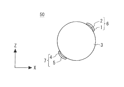
semiconductor covered with the insulating material and thereby to capture an
electron, wherein
the first electrode layer includes a first metal electrode and a n-type metal
oxide semiconductor
layer disposed between the first metal electrode and the charging element,
wherein the n-type
metal oxide semiconductor layer is positioned in contact with the charging
element, the second
electrode layer includes a second metal electrode and a p-type metal oxide
semiconductor layer
disposed between the second metal electrode and the charging element, wherein
the p-type metal
oxide semiconductor layer is positioned in contact with the charging element,
the charging
element has a spherical shape, and the first electrode layer and the second
electrode layer are
formed on a surface of the charging element, wherein a surface of at least one
of the first and
second electrode layers that is in contact with the charging element is a
curved surface.
[0006]
A battery according to another aspect of the present invention includes: a
first electrode
layer; a second electrode layer; and a charging element to which a charging
voltage between the
first and second electrode layers is applied, the charging element being
configured to form an
energy level in a band gap by causing a photoexcited structural change of an n-
type metal oxide
semiconductor covered with an insulating substance and thereby to capture an
electron, in which a
surface of at least one of the first and second electrode layers that is in
contact with the charging
element is a curved surface.
[0007]
In the above-described battery, the charging element may have a spherical
shape or a
cylindrical shape.
CA 2932306 2019-02-06
2a
[0008]
A battery according to another aspect of the present invention includes: a
first electrode
layer; a second electrode layer; and a charging element to which a charging
voltage between the
first and second electrode layers is applied, the charging element being
configured to form an
energy level in a band gap by causing a photoexcited structural change of an n-
type
metal oxide semiconductor covered with an insulating substance and thereby to
capture an
electron, in which at least one of the first and second electrode layers is
disposed inside the
charging element.
[0009]
In the above-described battery, the charging element may be formed in a
cylindrical
shape. Further, the first electrode layer may be disposed inside the charging
element and the
second electrode layer may be disposed on an outer circumference surface of
the charging
element.
[0010]
A battery according to another aspect of the present invention includes: a
first electrode
layer; a second electrode layer; and a charging element to which a charging
voltage between the
first arid second electrode layers is applied, the charging element being
configured to form an
energy level in a band gap by causing a photoexcited structural change of an n-
type metal oxide
semiconductor covered with an insulating substance and thereby to capture an
electron, in which
the charging element is formed in a three-dimensional shape.
[0011]
A battery according to another aspect of the present invention includes; a
first electrode
CA 2932306 2019-02-06
CA 02932306 2016-05-31
3
layer; a second electrode layer; and a charging element to which a charging
voltage between the
first and second electrode layers is applied, the charging element being
configured to form an
energy level in a band gap by causing a photocxcited structural change of an n-
type metal oxide
semiconductor covered with an insulating substance and thereby to capture an
electron, in which
the second electrode layer is disposed on a surface of the charging element
where the first
electrode is disposed.
In the above-described battery, a plurality of second electrode layers may he
provided,
and a second electrode layer that is opposed to the first electrode layer with
the charging element
interposed therebetween may be further provided.
[0012]
A battery according to another aspect of the present invention includes: a
first electrode
layer; a second electrode layer; and a charging element to which a charging
voltage between the
first and second electrode layers is applied, the charging element being
configured to form an
energy level in a band gap by causing a photoexcited structural change of an n-
type metal oxide
semiconductor covered with an insulating substance and thereby to capture an
electron, in which
the second electrode layer is disposed in a place different from that of the
first electrode layer in
a plane view, the plane being along a surface of the charging element.
[0013]
In the above-described battery, the second electrode layer may be formed on a
surface
of the charging element where the first electrode layer is formed.
[001,11
In the above-described battery, the second electrode layer may be formed on an
opposite
surface to a surface of the charging element where the first electrode layer
is formed.
[0015]
A battery according to another aspect of the present invention includes: a
first unit
battery; and a second unit battery connected with the first unit battery in
parallel or in series, in
which the first unit battery is the above-described battery, and the second
unit battery includes: a
first electrode layer; a second electrode layer; and a charging element to
which a charging
voltage between the first and second electrode layers is applied, the charging
element being
configured to form an energy level in a band gap by causing a photoexcited
structural change of
an n-type metal oxide semiconductor covered with an insulating substance and
thereby to capture
an electron.
[0016]
In the above-described battery, the first unit battery may be the above-
described battery
CA 02932306 2016-05-31
4
and the second unit battery may be a parallel-plate type unit battery.
[0017]
A battery according to another aspect of the present invention is a battery in
which each
of the first and second unit batteries is the above-described battery and the
first and second unit
= 5 batteries are stacked.
Advantageous Effects of Invention
[0018]
According to the present invention, an excellent battery can be provided.
Brief Description of Drawings
[0019]
Fig. 1 is a perspective view showing a fundamental configuration of a quantum
battery;
Fig. 2 is a cross section showing a fundamental configuration of a quantum
battery;
Fig. 3 is a schematic plane view of a battery used in a verification
experiment fur an
electron seepage phenomenon;
Fig. 4 is a figure for explaining an electron seepage phenomenon;
Fig. 5 is a figure for explaining an electron seepage phenomenon;
Fig. 6 is a figure for explaining an electron seepage phenomenon;
Fig. 7 is a figure for explaining an electron seepage phenomenon;
Fig. 8 is a perspective view showing a quantum battery according to
Configuration
Example 1;
Fig. 9 is a cross section showing the quantum battery according to
Configuration
Example 1;
Fig. 10 is a plane view showing the quantum battery according to Configuration
Example 1;
Fig. 11 is a perspective view showing a quantum battery according to
Configuration
Example 2;
Fig. 12 is a cross section showing the quantum battery according to
Configuration
Example 2;
Fig. 13 is a plane view showing the quantum battery according to Configuration
Example 2;
Fig. 14 is a perspective view showing a quantum battery according to
Configuration
Example 3;
CA 02932306 2016-05-31
Fig. 15 is a cross section showing the quantum battery according to
Configuration
Example 3;
Fig. 16 is a plane view showing the quantum battery according to Configuration
Example 3;
Fig. 17 is a cross section showing a quantum battery according to
Configuration
Example 4;
Fig. 18 is a perspective view showing a quantum battery according to
Configuration
Example 5;
Fig. 19 is a perspective view showing a quantum battery according to
Configuration
Example 6;
Fig. 20 is a cross section showing Stacked Structure I of a quantum battery
unit;
Fig. 21 is a cross section showing Stacked Structure 2 of a quantum battery
unit;
Fig. 22 is a cross section showing Stacked Structure 3 of a quantum battery
unit; and
Fig. 23 is a cross section showing Stacked Structure 4 of a quantum battery
unit.
Description of Embodiments
[0020]
Exemplary embodiments according to the present invention are explained with
reference to the drawings. Exemplary embodiments explained below are mere
examples
according to the present invention, and the present invention is not limited
to the below-shown
exemplary embodiments. Note that components/structures having the same symbols
in the
following specification and the drawings indicate mutually identical
components/structures.
[0021]
(A) Regarding quantum battery
The battery according to each exemplary embodiment explained below is a
battery to
which the quantum battery technology is applied. Therefore, a quantum battery
is briefly
explained hereinafter before explaining each exemplary embodiment.
[0022]
A quantum battery means a battery (secondary battery) that, in principle,
forms an
energy level in a band gap by utilizing a photoexeited structural change of a
metal oxide and
thereby captures electrons.
[0023]
The quantum battery is an all-solid type battery and functions as a battery on
its own.
Figs. 1 and 2 show an example of a configuration of a quantum battery. Note
that Fig. 1 is a
CA 02932306 2016-05-31
6
perspective view showing a configuration of a parallel-plate structure type
quantum battery 11,
and Fig. 2 is a cross section thereof, Note that in Figs. 1 and 2,
illustration of terminal members
such as a positive terminal and a negative terminal as well as packaging
elements such as an
outer sheath element and a covering element are omitted.
[0024]
The quantum battery 11 includes a charging element (charging layer) 3, a first
electrode
layer 6, and a second electrode layer 7. The charging element 3 is disposed
between the first and
second electrode layers 6 and 7. Therefore, a charging voltage generated
across the first and
second electrode layers 6 and 7 is applied to the charging element 3. The
charging element 3
accumulates (captures) electrons in a charging operation and releases the
accumulated electrons
in a discharging operation. The charging element 3 is a layer that keeps
electrons (accumulation
of electricity) when charging is not performed. The charging element 3 is
formed by applying a
photoexcited structural change technique.
[0025]
It should be noted that the photoexeited structural change is described, for
example, in
International Patent Publication No. W02008/053561, and is a phenomenon
(technique)
discovered by Akira Nakazawa, who is the inventor of the aforementioned patent
publication
(and also the inventor of the present application). In particular, Nakazawa
found out that when
effective excitation energy is given to a metal oxide that is a semiconductor
having a band gap of
a predetermined value or larger and having transparency and is covered with
insulating material,
a lot of energy levels in which no electron is present are generated in the
band gap. The quantum
battery 11 is charged by capturing electrons in those energy levels and is
discharged by releasing
the captured electrons.
[0026]
In the charging element 3, fine particles of an n-type metal oxide
semiconductor
covered with insulating material are deposited on the second electrode layer 7
in a thin-film state.
Then, the n-type metal oxide semiconductor undergoes a change by causing a
photoexcited
structural change by ultraviolet irradiation so that it can accumulate
electrons. The charging
element 3 includes a plurality of fine particles of an n-type metal oxide
semiconductor covered
with insulating material.
[0027]
The first electrode layer 6 is, for example, a negative electrode layer, and
includes a first
electrode 1 and an n-type metal oxide semiconductor layer 2. The n-type metal
oxide
semiconductor layer 2 is disposed between the first electrode 1 and the
charging element 3.
CA 02932306 2016-05-31
7
Therefore, one of the surfaces of the n-type metal oxide semiconductor layer 2
is in contact with
the first electrode 1 and the other surface is in contact with the charging
element 3.
[0028]
In the charging element 3, the insulating coating that covers the fine
particles of the n-
type metal oxide semiconductor is not necessarily uniform coating. When the
coating is not
formed, the n-type metal oxide semiconductor in the charging element 3 is
exposed, The n-type
metal oxide semiconductor layer 2 functions as an insulating layer that
insulates the n-type metal
oxide semiconductor in the charging layer from the first electrode 1 and is
provided to improve
properties such as the charging capacity. Further, the n-type metal oxide
semiconductor layer 2
provides an effective structure for reducing the characteristic variations of
the finished element,
thereby improving the stability and the yield in the manufacturing line.
[0029]
The second electrode layer 7 is, for example, a positive electrode layer, and
includes a
second electrode 5 and a p-type metal oxide semiconductor layer 4, The p-type
metal oxide
semiconductor layer 4 is disposed between the second electrode 5 and the
charging element 3.
Therefore, one of the surfaces of the p-type metal oxide semiconductor layer 4
is in contact with
the charging element 3 and the other surface is in contact with the second
electrode 5. The p-
type metal oxide semiconductor layer 4 is provided to prevent electrons from
flowing from the
second electrode 5 into the charging element 3.
[0030]
Each of the first and second electrodes 1 and 5 needs to be formed of
conductive
material. Examples of Metal electrodes that can be used for them include a
silver (Ag) alloy film
containing aluminum (Al), For the n-type metal oxide semiconductor layer 2,
titanium dioxide
(Ti02), tin oxide (S1102), or zinc oxide (Z110) may be used as its material.
For the p-type metal
oxide semiconductor layer 4, nickel oxide (NiO), copper aluminum oxide
(CuA102), or the like
can be used as its material.
[0031]
Note that although the first electrode layer 6 has a two-layer structure
composed of the
first electrode 1 and the n-type metal oxide semiconductor layer 2 according
to the above
explanation, the structure of the first electrode layer 6 is not limited to
the two-layer structure.
For example, the first electrode layer 6 may be a single-layer structure
composed of the first
electrode 1 alone. Similarly, the structure of the second electrode layer 7 is
not limited to the
two-layer structure composed of the p-type metal oxide semiconductor layer 4
and the second
electrode 5. For example, the second electrode layer 7 may be a single-layer
structure composed
CA 02932306 2016-05-31
8
of the second electrode 5 alone. That is, each of the first and second
electrode layers 6 and 7
may be composed of a metal electrode alone.
[0032]
(B) Electron seepage phenomenon
It has been believed that in quantum batteries like the one shown in Figs. 1
and 2,
electrons accumulate only in the charging element 3 disposed between the first
and second
electrode layers 6 and 7 during the charging. That is, it has been believed
that electrons
accumulate only in the area directly below the second electrode layer 7 in the
charging clement 3.
However, experiments carried out by the inventors of the present application
have shown a
phenomenon that when the area directly below the second electrode layer 7 is
fully filled with
electrons, electrons seep out to the outside of the area directly below the
second electrode layer 7.
That is, it has been shown that electrons seep out to the outside of the area
directly below the
second electrode layer 7 and accumulate there.
[0033]
The electron seepage phenomenon, which has been discovered by the inventors of
the
present application, is explained hereinafter. A quantum battery 10 like the
one shown in Fig. 3
was used to discover the electron seepage phenomenon. Note that Fig. 3 is an
XY-plane view
schematically showing a pattern shape of a second electrode layer 7 disposed
on a charging
element 3.
[0034]
In Fig. 3, a plurality of rectangular second electrode layers 7 are arranged
in an array.
That is, a plurality of rectangular second electrode layers 7 are arranged
along the X-direction
and the Y-direetion. There are areas where no second electrode layer 7 is
disposcd between
neighboring second electrode layers 7. Meanwhile, assume that a first
electrode layer 6 (which
is not shown in Fig. 3) is formed on substantially the entire surface of the
charging element 3.
[0035]
Here, a second electrode layer 7 to which a charging voltage is applied is
referred to as
"section 7a" hereinafter. That is, no charging voltage is applied to the
sections other than the
section 7a. Then, a voltage at each section when the section 7a is being
charged and when the
section 7a is in a natural discharging state was measured.
[0036]
As the charging to the section 7a continues, the voltage in a section 7b
located near the
section 7a increases. That is, a voltage occurs in the section 7b, to which no
charging voltage is
applied, based on the electrons accumulated in the charging element 3.
Further, even after the
CA 02932306 2016-05-31
9
charging to the section 7a is stopped, the voltage in the section 71) rises
while the voltage in the
section 7a decreases due to the natural discharging. This experiment shows
that electrons seep
out from the charged place to the area around the charged place.
[0037]
Figs. 4 to 7 show models for explaining the electron seepage phenomenon in the
quantum battery 10. In Figs. 4 to 7, the first electrode layer 6 is formed on
the entire surface of
the charging element 3 and the second electrode layer 7 is formed in a part of
the surface of the
charging element 1 Note that the area where the second electrode layer 7
overlaps the first
electrode layer 6 is referred to as "overlap area 18" and the area where they
do not overlap is
referred to as "non-overlap area 19".
[0038]
Firstly, as shown in Fig. 4, a power supply 31 is connected across the first
and second
electrode layers 6 and 7 to generate a charging voltage in order to charge the
quantum battery 10.
The charging voltage between the first and second electrode layers 6 and 7 is
applied to the
charging element 3. During the charging of the quantum battery 10, electrons
first start to
accumulate in the area directly below the second electrode layer 7 (indicated
by letters "e'' in the
figure). That is, electrons accumulate in the overlap area 18. Then, as shown
in Fig. 5, when the
overlap area 18 is fully filled with electrons, electrons start to accumulate
in the outside of the
area directly below the second electrode layer 7. That is, electrons diffuse
from the overlap area
18 to the non-overlap area 19.
[0039]
After that, as shown in Fig. 6, electrons diffuse throughout the charging
element 3 until
the potential is settled. That is, the density of electrons in the charging
clement 3 becomes
uniform. As a result, the electron density in the overlap area 18 becomes
substantially equal to
that in the non-overlap area 19. During the discharging, as shown in Fig. 7,
electrons located in
the area directly below the second electrode layer 7 first escape, and then
electrons located
outside the area directly below the second electrode layer 7 gradually escape.
That is, when the
discharging starts, the electron density in the overlap area 18 becomes lower
than that in the non-
overlap area 19.
[0040]
In the past, it has been believed that electrons accumulate only in the area
directly below
the second electrode layer 7. Therefore, parallel-plate structures in which
both the first and
second electrode layers 6 and 7 are formed on substantially the entire surface
of the charging
element 3 have been used. However, the electron seepage phenomenon enables an
electrode
CA 02932306 2016-05-31
layer(s) to be disposed on part of the surface of the charging element 3.
Further, even when the
electrode layer(s) is formed on part of the surface of the charging element 3,
the same power
capacity as that in the case where the electrode layer(s) is formed on the
entire surface can be
achieved, provided that the volume of the charging element 3 is the same as
that in the above
5 latter case. That is, when the quantum battery is charged to 100%, the
electron density in the
non-overlap area 19 becomes substantially equal to that in the overlap area
18. Therefore, it is
possible to improve properties of the battery while maintaining its
fundamental functions as a
battery.
[0041]
10 (C) Single-layer quantum battery
As described above, quantum batteries having various configurations can be
realized by
the electron seepage phenomenon. Configuration Examples of quantum batteries
are explained
hereinafter. In the following explanation, a single quantum battery is
explained.
[0042]
(C-1) Configuration Example 1
Fig. 8 is a perspective view showing a quantum battery 20 according to
Configuration
Example 1 and Fig. 9 is a cross section thereof. Further, Fig. 10 is a plane
view of the quantum
battery 20. In Configuration Example 1, the charging element 3 is a charging
layer formed into a
plate or a sheet. That is, two opposite surfaces of the charging element 3 are
parallel planes. A
first electrode layer 6 is formed on the bottom surface of the charging
element 3 and a second
electrode layer 7 is formed on the top surface thereof. That is, the first and
second electrode
layers 6 and 7 are formed on different surfaces of the charging element 3.
[0043]
As shown in Fig. 10, the charging element 3 is formed in a rectangular shape
in the XY-
plane view. The positions of the first and second electrode layers 6 and 7 are
shifted from each
other in the XY-plane view. In this example, the first and second electrode
layers 6 and 7 are
formed in narrow rectangular shapes whose longitudinal direction is in the Y-
direction. Further,
the first electrode layer 6 is disposed on the positive end in the X-direction
of the charging
element 3 and the second electrode layer 7 is disposed on the negative end in
the X-direction
thereof. As described above, the first electrode layer 6 is disposed near one
end of the charging
element 3 in the X-direction and the second electrode layer 7 is disposed near
the other end of
the charging element 3 thereof.
[0044]
When a charging voltage is applied across the first and second electrode
layers 6 and 7,
CA 02932306 2016-05-31
11
electric lines of force occur in the charging element 3 as shown in Fig. 9.
Electrons accumulate
in the charging element 3 by the charging voltage between the first and second
electrode layers 6
and 7. Further, because of the above-described electron seepage phenomenon,
electrons
accumulate throughout the charging element 3. As described above, even when
the positions of
the first and second electrode layers 6 and 7 are shifted from each other in
the X-direction,
electrons accumulate throughout the charging element 3.
[0045]
Since the first and second electrode layers 6 and 7 are fonned only on parts
of the
charging element 3, the volumetric efficiency of the battery can be improved.
In general, the
volumetric efficiency of a battery is expressed by an expression "(Volumetric
efficiency of
battery) ¨ (Effective volume of battery)/(Total volume of battery)".
Therefore, the volumetric
efficiency can be improved by reducing the total volume of the quantum battery
20. As shown
above, since the electrode layers are reduced in size, the volumetric
efficiency can be improved.
Further, since the first and second electrode layers 6 and 7 are partially
formed on the surface of
the charging element 3, the weight of the quantum battery 20 can be reduced in
comparison to
the case where the first and second electrode layers 6 and 7 are formed on the
entire surface of
the charging element 3.
[0046]
(C-2) Configuration Example 2
Fig. 11 is a perspective view showing a quantum battery 30 according to
Configuration
Example 2 and Fig. 12 is a cross section thereof. Further, Fig. 13 is a plane
view of the quantum
battery 30. In Configuration Example 2, the charging element 3 is a charging
layer formed into a
plate or a sheet. That is, two opposite surfaces of the charging element 3 are
parallel planes.
Configuration Example 2 is different from Configuration Example 1 hi regard to
the position of
the first electrode layer 6. The first and second electrode layers 6 and 7 are
both formed on the
top surface of the charging element 3. The second electrode layer 7 is
disposed on the surface of
the charging element 3 where the first electrode layer 6 is disposed. The
first and second
electrode layers 6 and 7 are formed on the same plane of the charging element
3.
[0047]
As shown in Fig. 13, the charging element 3 is formed in a rectangular shape
in the XY-
plane view. Further, the positions of the first and second electrode layers 6
and 7 are shified
from each other in the XY-plane view. In this example, the first and second
electrode layers 6
and 7 are formed in narrow rectangular shapes whose longitudinal direction is
in the Y-direction.
Further, the first electrode layer 6 is disposed on the positive end in the X-
direction of the
CA 02932306 2016-05-31
1')
charging clement 3 and the second electrode layer 7 is disposed on the
negative end in the X-
direction. As described above, the first electrode layer 6 is disposed near
one end of the charging
element 3 and the second electrode layer 7 is disposed near the other end
thereof in the XY-plane
view. In the quantum battery 30, the second electrode layer 7 is disposed in a
place different
from that of the first electrode layer 6 in the XY-plane view.
[0048]
When a charging voltage is applied across the first and second electrode
layers 6 and 7,
electric lines of force occur in the charging element 3 as shown in Fig. 12.
As a result, electrons
accumulate in the charging element 3 by the charging voltage between the first
and second
electrode layers 6 and 7. Further, because of the above-described electron
seepage phenomenon,
electrons accumulate throughout the charging element 3. As described above,
even when the
first and second electrode layers 6 and 7 are disposed on the same plane of
the charging element
3 and are disposed in different positions in the X-direction, electrons
accumulate throughout the
charging element 3.
[0049]
Since the first and second electrode layers 6 and 7 are formed only on a
part(s) of the
charging clement 3, the volumetric efficiency of the battery can be improved.
In general, the
volumetric efficiency of a battery is expressed by an expression "(Volumetric
efficiency of
battery) = (Effective volume of battery)/(Total volume of battery)".
Therefore, the volumetric
efficiency can be improved by reducing the total volume of the quantum battery
30. As shown
above, since the electrode layer is reduced in size, the volumetric efficiency
can be improved.
Further, since the first and second electrode layers 6 and 7 are partially
formed in the charging
element 3, the weight of the quantum battery 30 can be reduced in comparison
to the ease where
the first and second electrode layers 6 and 7 are formed on the entire surface
of the charging
element 3.
[0050]
(C-3) Configuration Example 3
Fig. 14 is a perspective view showing a quantum battery 40 according to
Configuration
Example 3 and Fig. 15 is a cross section thereof. Further, Fig. 16 is a plane
view of the quantum
battery 40. In Configuration Example 3, the charging element 3 is a charging
layer formed into a
plate or a sheet. That is, two opposite surfaces of the charging element 3 are
parallel planes.
First and second electrode layers 6 and 7 are both formed on each of the top
surface and the
bottom surface of the charging element 3.
[0051]
CA 02932306 2016-05-31
13
More specifically, the quantum battery 40 includes two first electrode layers
6 and two
second electrode layers 7. In the tbllowing explanation, the two first
electrode layers 6 are
referred to as "first electrode layer 6a" and "first electrode layer 6b"
respectively, and the two
second electrode layers 7 are referred to as "second electrode layer 7a" and
"second electrode
layer 7b," respectively. The first electrode layer 6a and the second electrode
layer 7a are formed
on the top surface of the charging element 3. The first electrode layer 6b and
the second
electrode layer 7b are formed on the bottom surface of the charging element 3.
The first
electrode layer 6a is disposed on the positive end in the X-direction of the
charging element 3
and the first electrode layer 6b is disposed on the negative end in the X-
direction thereof.
[0052]
The second electrode layer 7a is disposed on the negative end in the X-
direction of the
charging element 3 and the second electrode layer 7b, which is formed on the
bottom surface of
the charging element 3, is disposed on the positive end in the X-direction
thereof. The second
electrode layer 7a and the first electrode layer 6b are disposed so as to be
opposed to each other
.. with the charging element 3 interposed therebetween. That is, the position
of the second
electrode layer 7a coincides with that of the first electrode layer 6b on the
XY-plane. The
second electrode layer 7b and the first electrode layer 6a are disposed so as
to be opposed to each
other with the charging clement 3 interposed therebetween. That is, the
position of the second
electrode layer 7b coincides with that of the first electrode layer 6a on the
XY-plane.
[0053]
Therefore, the second electrode layer 7 of the quantum battery 40 includes the
second
electrode layer 7a, which is disposed in a different position from that of the
first electrode layer
6a in the XY-plane view, and the second electrode layer 7b, which is disposed
in the same
position as that or the first electrode layer 6a in the XY-plane view.
Similarly, the first electrode
layer 6 of the quantum battery 40 includes the first electrode layer 6b, which
is disposed in the
same position as that of the second electrode layer 7a in the XY-plane view,
and the first
electrode layer 6a, which is disposed in a different position from that of the
second electrode
layer 7a in the XY-plane view.
[0054]
When a charging voltage is applied across the first and second electrode
layers 6 and 7,
electrons accumulate in the charging element 3 by the charging voltage between
the first and
second electrode layers 6 and 7. Further, because of the above-described
electron seepage
phenomenon, electrons accumulate throughout the charging element 3. As
described above,
even when the first and second electrode layers 6 and 7 are disposed on the
same plane of the
CA 02932306 2016-05-31
14
charging element 3 and in different positions in the X-direction, electrons
accumulate throughout
the charging element 3.
[0055]
Further, in Configuration Example 3, each of the first and second electrode
layers 6 and
7 is divided into and formed as a plurality of sections. Therefore, it is
possible to use first and
second electrode layers 6 and 7 in the charging process which are different
from those used in
the discharging process. For example, when the quantum battery is charged, a
power supply is
connected to all of the first electrode layers 6a and 6b and the second
electrode layers 7a and 7b
to apply a charging voltage to the battery. This enables a fast charging
operation. Meanwhile,
when the quantum battery is discharged, a load(s) or the like is connected
only to the first
electrode layer 6a and the second electrode layer 7b. In this way, it is
possible to limit the
electric power that is drawn out at once, thus enabling long-time discharging.
[0056]
As described above, by forming a plurality of divided sections of electrode
layers, it is
possible to change the size of the overlap area between that in the charging
process and that in
the discharging process. For example, the size of the overlap area in the
charging process can be
reduced in comparison to that in the discharging process. Alternatively, the
size of the overlap
area in the charging process can be increased in comparison to that in the
discharging process.
Desired charging/discharging characteristics can be achieved by dividing the
first electrode layer
6 or the second electrode layer 7 into a plurality of sections.
[0057]
(C-4) Configuration Example 4
Fig. 17 is a cross section showing a quantum battery 50 according to
Configuration
Example 4. The quantum battery 50 is formed in a three-dimensional shape in
Configuration
Example 4. Specifically, the quantum battery 50 includes a charging element 3
formed in a
spherical shape. Further, first and second electrode layers 6 and 7 are formed
on parts of the
spherical charging element 3. The first and second electrode layers 6 and 7
are formed on part of
the surface of the charging element 3.
[0058]
The first and second electrode layers 6 and 7 are disposed so as to be opposed
to each
other with the charging element 3 interposed therebetween. In this example,
the first and second
electrode layers 6 and 7 are disposed to be opposed to each other so that the
center of the
spherical charging element 3 is positioned between the first and second
electrode layers 6 and 7.
In this case, when a charging voltage is applied across the first and second
electrode layers 6 and
CA 02932306 2016-05-31
7, electrons accumulate in the charging element 3 by the charging voltage
between the first and
second electrode layers 6 and 7. Further, because of the above-described
electron seepage
phenomenon, electrons accumulate throughout the charging element 3. As
described above,
electrons spread throughout the spherical charging element 3.
5 [00591
The first and second electrode layers 6 and 7 are formed on the surface of the
spherically-formed charging element 3. Therefore, the surface of the charging
element 3 is
formed in a spherical shape. For at least one of the first and second
electrode layers 6 and 7, the
surface that is in contact with the charging element 3 is a curved surface.
Further, the exterior
10 surface of the charging element 3 is a curved surface. The volumetric
efficiency can be
improved by forming the charging element 3 in a three-dimensional shape.
Further, since the
first and second electrode layers 6 and 7 are formed on part of the surface of
the charging
element 3, the weight of the quantum battery 50 can be reduced.
[0060]
15 (C-5) Configuration Example 5
Fig. 18 is a perspective view showing a quantum battery 60 according to
Configuration
Example 5. In Configuration Example 5, the quantum battery 60 has a coaxial
configuration.
Therefore, the charging element 3 is formed in a cylindrical shape. A
cylindrical first electrode
layer 6 is disposed at the center of the charging element 3. The outer
circumference surface of
the first electrode layer 6, which is located along the central axis, is in
contact with the charging
element 3. One end of the first electrode layer 6 is positioned outside the
charging element 3 so
that it can be connected to an external terminal.
[0061]
A second electrode layer 7 is disposed on the outer circumference surface of
the
charging element 3. Therefore, the surface of the charging element 3 that is
in contact with the
first electrode layer 6 or the second electrode layer 7 is a curved surface.
When a charging
voltage is applied across the first and second electrode layers 6 and 7,
electrons spread
throughout the cylindrical charging element 3. Note that although the second
electrode layer 7 is
formed on the entire area of the outer circumference surface of the charging
element 3 in Fig. 18,
the second electrode layer 7 may be partially formed on the outer
circumference surface. That is,
the second electrode layer 7 may be formed on a part(s) of the outer
circumference surface of the
charging element 3. In this case, a plurality of sections of second electrode
layers 7 can be
formed on the outer circumference surface of the charging element 3.
[0062]
CA 02932306 2016-05-31
16
Further, the first electrode layer 6 may have such a length in the X-direction
that it
extends only to some midpoint in the charging element 3. Needless to say, the
positions of the
first and second electrode layers 6 and 7 may he interchanged. That is, the
first electrode layer 6
may be formed on the outer side of the charging element 3 and the second
electrode layer 7 may
be formed on the inner side of the charging element 3.
[0063]
The charging clement 3 is formed on the outer circumference surface of the
cylindrical
first electrode layer 6. Further, the second electrode layer 7 is formed on
the outer circumference
surface of the charging element 3. The surface of the charging element 3 is a
curved surface.
For at least one of the first and second electrode layers 6 and 7, the surface
that is in contact with
the charging element 3 is a curved surface. The volumetric efficiency can be
improved by
forming the charging element 3 in a three-dimensional shape. Further, since
the first and second
electrode layers 6 and 7 are formed on part of the charging element 3, the
weight of the quantum
battery 60 can be reduced.
[0064]
(C-6) Configuration Example 6
Fig. 19 is a perspective view showing a quantum battery 70 according to
Configuration
Example 6. In the quantum battery 70, the first and second electrode layers 6
and 7 are disposed
inside the charging element 3. One end of each of the first and second
electrode layers 6 and 7 is
positioned outside the charging element 3 so that they can be connected to
external terminals. In
this example, each of the first and second electrode layers 6 and 7 is formed
in a cylindrical
shape whose longitudinal direction is in the Y-direction. The charging element
3 is formed in a
rectangular parallelepiped shape with the first and second electrode layers 6
and 7 disposed
inside thereof. Needless to say, the shapes of the first and second electrode
layers 6 and 7 and
the charging clement 3 are not restricted to any particular shapes.
[0065]
A part of the charging element 3 is disposed between the first and second
electrode
layers 6 and 7. When a charging voltage is supplied across the first and
second electrode layers
6 and 7, a voltage is applied in the charging element 3. As the charging
continues, electrons
spread from the area between the first and second electrode layers 6 and 7 to
the entire area of
the charging element 3. Because of the above-described electron seepage
phenomenon,
electrons accumulate throughout the charging element 3.
[0066]
Note that although the first and second electrode layers 6 and 7 are both
disposed inside
CA 02932306 2016-05-31
17
the charging element 3 in Fig. 19, only one of the first and second electrode
layers 6 and 7 may
be disposed inside the charging element 3. In this case, the other electrode
layer may be formed
on the surface of the charging element 3.
[0067]
In Configuration Examples 1 to 3, the electrode layers are folined on part of
the surface
of the plate-like or sheet-like charging element 3. By using such
configurations, various
packaging configurations can be realized. As a result, it is possible to
improve the volumetric
efficiency of the quantum battery and/or to reduce the weight and/or the cost
of the quantum
battery.
[0068]
In Configuration Examples 4 to 6, the charging element 3 is formed in a three-
dimensional shape. The volume of the charging element 3 can be increased by
forming the
charging element 3 in a three-dimensional shape. That is, the battery capacity
can be increased
by using a charging element 3 having a large thickness. For example, when a
plate-like or sheet-
like charging layer is used, the area (i.e., two-dimensional size) of the
charging layer needs to be
increased to increase the volume of the charging layer. However, it could be
difficult to increase
the size of the charging layer in view of its uniformity. As explained above
in this exemplary
embodiment, it is possible to realize a quantum battery having a high battery
capacity and
excellent properties by using a three-dimensional charging element 3. Further,
various
packaging configurations can be realized by forming the charging element 3 in
a three-
dimensional shape. As a result, it is possible to improve the volumetric
efficiency of the
quantum battery and/or to reduce the weight and/or the cost of the quantum
battery.
[0069]
Various forming (or molding) methods can be used as a method for forming a
charging
element 3 in a three-dimensional shape. For example, a charging element 3 can
be molded by
using a mold having a desired shape. Specifically, fine particles of an n-type
metal oxide
semiconductor covered with insulating material are put into a mold. Then,
after they are pressed
and compacted, they are baked. By doing so, a charging element 3 having an
arbitrary shape can
be molded. It is possible to form a section(s) having a large thickness in the
charging element 3
by using a mold having a desired shape, and thereby to form the charging
element 3 in a three-
dimensional shape. Further, in Configuration Examples 5 and 6, the charging
element 3 is
molded with an electrode layer(s) disposed inside thereof.
[0070]
(D) Stacked structure of quantum battery
CA 02932306 2016-05-31
18
In each of Configuration Examples 1-6, a single quantum battery is shown.
However, it
is possible to increase the capacity by combining a plurality of quantum
batteries. A quantum
battery including a plurality of single quantum batteries each of which may he
one of the
quantum batteries shown in Configuration Examples 1 to 6 is explained
hereinafter. Hereinafter,
a single quantum battery is also referred to as "unit quantum battery" and a
quantum battery
including a plurality of unit quantum batteries is also referred to as
"quantum battery unit". It is
possible to improve the volumetric efficiency of a quantum battery and/or to
reduce the weight
and/or the cost of a quantum battery even further by connecting a plurality of
unit quantum
batteries in parallel or in series.
[0071]
(D-1) Stacked Structure 1 of quantum battery unit
Fig. 20 is a cross section showing a quantum battery unit 100 according to
Stacked
Structure I. In Fig. 20, two quantum batteries 20 each of which is shown in
Configuration
Example 1 arc used. In Fig. 20, the quantum batteries 20 are referred to as
unit quantum
batteries 20a and 20b, respectively. The unit quantum batteries 20a and 20b
are connected in
series.
[0072]
In Fig. 20, sheet-like or plate-like unit quantum batteries 20a and 20b are
stacked on one
another. That is, charging elements 3a and 3b are arranged in parallel with
each other. Further,
a first electrode layer 6a of the unit quantum battery 20a and a second
electrode layer 7b of the
unit quantum battery 20b are disposed between the charging elements 3a and 3b.
A first
electrode layer 6b is connected to a negative terminal 101 and a second
electrode layer 7a is
connected to a positive terminal 102. Further, the first electrode layer 6a is
connected to the
second electrode layer 7b. The first electrode layer 6a is connected to the
second electrode layer
7b through, for example, a connection teinlinal(s) (not shown). Alternatively,
the first electrode
layer 6a may be connected to the second electrode layer 7b by forming a
conductive pattern on
the charging element 3a or 3b. Further, an insulating layer may be provided to
prevent the first
electrode layer 6a from coming into contact with the charging element 3b or
the second electrode
layer 7b from coming into contact with the charging element 3a.
[0073]
As described above, the output voltage can be increased by connecting two unit
quantum batteries 20a and 20b in series. Further, owing to the partial
electrode configuration,
the volumetric efficiency of the quantum battery unit 100 can be improved.
Since the terminal
structure can be simplified, the volumetric efficiency can be improved.
Further, since the sizes
CA 02932306 2016-05-31
19
of the first and second electrode layers 6 and 7 are small, the weight can be
reduced.
[0074]
Needless to say, a stacked structure composed of three layers or more may be
adopted
for the quantum battery unit 100. For example, such a stacked structure can be
easily realized by
disposing two or more structures each of which is shown in Fig. 20 in a
repetitive fashion. The
output voltage of the quantum battery unit 100 is expressed as "NxV" and the
current capacity of
the quantum battery unit 100 is expressed as "Ah", where V is the voltage of
the unit quantum
battery 20, Ah is the current capacity of the unit quantum battery 20 and N is
the number of
stacked layers.
[0075]
(1)-2) Stacked Structure 2 of quantum battery unit
Fig. 21 is a cross section showing a quantum battery unit 200 according to
Stacked
Structure 2. In Fig. 21, two quantum batteries 20 each of which is shown in
Configuration
Example 1 arc used. In Fig. 21, the quantum batteries 20 are referred to as
unit quantum
.. batteries 20a and 20b, respectively. The unit quantum batteries 20a and 20b
are connected in
parallel. In Fig. 21, sheet-like or plate-like unit quantum batteries 20a and
20b are stacked on
one another. That is, charging elements 3a and 3b are arranged in parallel
with each other.
[0076]
Specifically, the unit quantum batteries 20a and 20b are arranged so that the
second
electrode layers 7a and 7b face each other. In other words, the second
electrode layer 7a is
disposed on the bottom surface of the charging element 3a and the second
electrode layer 7b is
disposed on the top surface of the charging element 3b. Further, a positive
terminal 102 is
disposed between the second electrode layers 7a and 7b. The positive terminal
102 is connected
to the second electrode layers 7a and 7b in a state where the positive
terminal 102 is sandwiched
between the second electrode layers 7a and 7b. By using this configuration,
the unit quantum
batteries 20a and 20b can share the positive terminal 102, thus making it
possible to simplify the
terminal structure. Further, in Fig. 21, the quantum battery is formed so that
the second
electrode layer 7 does not protrude from the surface of the charging element
3.
[0077]
Meanwhile, the first electrode layer 6a is disposed on the top surface of the
charging
element 3a and the first electrode layer 6b is disposed on the bottom surface
of the charging
element 3b. Further, a negative terminal 101 is connected to the first
electrode layers 6a and 6b.
The negative terminal 101 branches off so as to connect to each of the first
electrode layers 6a
and 6b.
CA 02932306 2016-05-31
[0078]
The current capacity can be increased by connecting two unit quantum batteries
20a and
20b in parallel as shown above. Further, owing to the partial electrode
configuration, the
volumetric efficiency of the quantum battery unit 200 can be improved. Since
the terminal
5 structure can be simplified, the volumetric efficiency can be improved.
Further, since the sizes
of the first and second electrode layers 6 and 7 are small, the weight can be
reduced,
[0079]
Needless to say, a stacked structure composed of three layers or more may be
adopted
for the quantum battery unit 200. In this case, such a stacked structure can
be easily realized, for
10 example, by disposing two or more structures each of which is shown in
Fig. 21 in a repetitive
fashion. The current capacity of the quantum battery unit 200 is expressed as
"NxAh" and the
output voltage of the quantum battery unit 200 is expressed as "V", where V is
the output
voltage of the unit quantum battery 20, Ah is the current capacity of the unit
quantum battery 20
and N is the number of stacked layers.
15 .. [0080]
Note that although the unit quantum batteries 20 are stacked in the quantum
battery
units according to Stacked Structures 1 and 2, unit quantum batteries having
other configurations
may be stacked in other quantum battery units. For example, unit quantum
batteries 30 or unit
quantum batteries 40 may be stacked in other quantum battery units.
Alternatively, unit quantum
20 batteries 20, 30 and/or 40 having different configurations may be
stacked in other quantum
battery units. For example, a unit quantum battery 20 and a unit quantum
battery 30 may be
stacked, or a unit quantum battery 20 and a unit quantum battery 40 may be
stacked.
Alternatively, a unit quantum battery 30 and a unit quantum battery 40 may be
stacked.
Needless to say, three or more unit quantum batteries may be combined. In this
case, the current
capacity is expressed as "NxAh".
[0081]
Further, it is possible to combine two or more parallel-connected unit quantum
batteries
with two or more series-connected unit quantum batteries. For example, it is
possible to adopt a
configuration including 2N unit quantum batteries in which the number of
parallel connections is
N and the number of series connections is N. In this case, the output voltage
of the unit quantum
battery is expressed as "NxV" and the current capacity is expressed as "NxAh",
where V is the
voltage of the unit quantum battery and Ah is the current capacity of the unit
quantum battery,
[0082]
(D-3) Stacked Structure 3 of quantum battery unit
CA 02932306 2016-05-31
21
Fig. 22 is a cross section showing a quantum battery unit 300 according to
Stacked
Structure 3. In Fig. 22, the parallel-plate type quantum battery 11 shown in
Figs. 1 and 2 is
combined with the quantum battery 50 shown in Configuration Example 4. In Fig.
22, the
quantum battery unit 300 includes one unit quantum battery 11 and six unit
quantum batteries 50.
That is, three-dimensional unit quantum batteries 50 are combined with a
parallel-plate type unit
quantum battery 11.
[0083]
More specifically, three unit quantum batteries 50 are disposed on each
surface of a
quantum battery 11. The quantum battery unit 300 includes one unit quantum
battery 11 and six
unit quantum batteries 50. In Fig. 22, the unit quantum batteries 50 and the
unit quantum battery
11 included in the quantum battery unit 300 are referred to as unit quantum
batteries 50a to 50f
and a unit quantum battery 11g, respectively.
[0084]
The three-dimensional unit quantum batteries 50a to 50f are disposed on both
sides of
the sheet-like unit quantum battery 11g. That is, the parallel-plate type unit
quantum battery 11
is disposed between the three-dimensional unit quantum batteries 50. The unit
quantum batteries
50a to 50c are arranged in a row along the X-direction. The unit quantum
batteries 50d to 50f
are also arranged in a row along the X-direction.
[0085]
The unit quantum batteries 50a, 50b and 50c are disposed above the (on +Z
side) of the
unit quantum battery llg, and the unit quantum batteries 50d, 50e and 50f are
disposed below
the (on -Z side) of the unit quantum battery 11 g. The unit quantum battery
11g and the unit
quantum batteries 50a to 50f are connected in parallel. Therefore, the
positive terminal 102 is
connected to each of the second electrode layers 7a to 7g and the negative
terminal 101 is
connected to each of the first electrode layers 6a to 6g.
[0086]
A part of the positive terminal 102 is disposed above the second electrode
layer 7g.
Further, a part of the positive terminal 102 is also disposed below the second
electrode layers 72,
7b and 7c. Therefore, the positive terminal 102 is substantially disposed
between the second
electrode layer 7g and the second electrode layers 7a, 7b and 7c. By using
this configuration, the
common positive terminal 102 can he connected to the second electrode layers
7a, 7b and 7c and
to the second electrode layer 7g. That is, the top surface of the plate-like
positive tenninal 102 is
in contact with the second electrode layers 7a, 7b and 7c and its bottom
surface is in contact with
the second electrode layer 7g. With this configuration, the terminal structure
can be simplified.
CA 02932306 2016-05-31
22
[0087]
A part of the negative terminal 101 is disposed below the first electrode
layer 6g.
Further, a part of the negative terminal 101 is also disposed above the first
electrode layers 6d, be
and 6f Therefore, the negative terminal 101 is substantially disposed between
the first electrode
layer bg and the first electrode layers bd, be and 6f. By using this
configuration, the common
negative terminal 101 can be connected to the first electrode layers 6d, be
and bf and to the first
electrode layer bg. That is, the bottom surface of the plate-like negative
terminal 101 is in
contact with the first electrode layers 6d, be and 6f and the top surface of
negative terminal 101
is in contact with the first electrode layer bg. With this configuration, the
terminal structure can
be simplified.
[0088]
In the configuration shown in Fig. 22, since the parallel-plate type unit
quantum battery
11 is used, the power density can be improved. In addition, since the unit
quantum batteries 50
each including the charging element 3 having a large volume is used, the
current capacity can be
improved. A battery having a large current capacity and a high power density
can be realized by
connecting a sheet-like quantum battery(ies) with a three-dimensional quantum
battery(ies).
Therefore, the quantum battery unit 300 having excellent properties can be
realized.
[0089]
Note that although the configuration in which the unit quantum batteries 50
are arranged
in a row on each surface of the unit quantum battery 11 is shown in Fig. 22,
the unit quantum
batteries 50 may be arranged in two or more rows. That is, the unit quantum
batteries 50 may be
arranged in a matrix. In this case, a plurality of unit quantum batteries 50
are arranged along the
X-direction and along the Y-direction. Further, the unit quantum batteries 50
may be arranged
on only one of the surfaces of the unit quantum battery 11. Further, it is
also possible to use any
.. one of the quantum batteries 20 to 40 shown in Configuration Examples 1, 2
and 3 as the
parallel-plate type unit quantum battery 11.
[0090]
(D-4) Stacked Structure 4 of quantum battery unit
Fig. 23 is a cross section showing a quantum battery unit 400 according to
Stacked
.. Structure 4. In Fig. 23, the parallel-plate type quantum battery 11 shown
in Fig. 1 is combined
with the quantum battery 50 shown in Configuration Example 4. In Fig. 23, the
quantum battery
unit 400 includes two unit quantum batteries 11 and three unit quantum
batteries 50,
[0091]
More specifically, one unit quantum battery 11 is disposed above the quantum
batteries
CA 02932306 2016-05-31
23
50 and the other unit quantum battery 11 is disposed below the quantum
batteries 50. That is,
the three-dimensional unit quantum batteries 50 are disposed between the
parallel-plate type unit
quantum batteries 11. In Fig. 23, the unit quantum batteries 50 and the unit
quantum batteries 11
included in the quantum battery unit 400 are referred to as unit quantum
batteries 50a to 50e and
unit quantum batteries lid and lie, respectively.
[0092.1
The three-dimensional unit quantum batteries 50a to 50c are disposed between
the
sheet-like unit quantum batteries lid and Ile, The unit quantum batteries 50a
to 50c are
arranged in a row along the X-direction. The unit quantum batteries lid and
lie and the unit
quantum batteries 50a to 50c are connected in parallel. Therefore, the
positive terminal 102 is
connected to each of the second electrode layers 7a to 7e and the negative
terminal 101 is
connected to each of the first electrode layers 6a to 6e.
[00931
The second electrode layer 7d is disposed on the top surface of the unit
quantum battery
lid and the first electrode layer 6d is disposed on the bottom surface of this
battery. The first
electrode layers 6a to 6c are disposed on the top side of the unit quantum
batteries 50a to 50c.
Further, a part of the negative terminal 101 is disposed between the first
electrode layers 6a to 6c
and the first electrode layer 6d. By using this configuration, the common
negative terminal 101
can be connected to the first electrode layers 6a, 6b and 6c and to the first
electrode layer 6d.
That is, the bottom surface of the plate-like negative terminal 101 is in
contact with the first
electrode layers 6a, 6b and 6c and its top surface is in contact with the
first electrode layer 6d.
With this configuration, the terminal structure can be simplified.
[0094]
The second electrode layer 7e is disposed on the top surface of the unit
quantum battery
lie and the first electrode layer 6e is disposed on the bottom surface of unit
quantum battery lie.
The second electrode layers 7a to 7c arc disposed on the bottom side of the
unit quantum
batteries 50a to 50c. Further, a part of the positive terminal 102 is disposed
between the second
electrode layers 7a to 7c and the second electrode layer 7e. By using this
configuration, the
common positive terminal 102 can be connected to the second electrode layers
7a to 7c and to
the second electrode layer 7e. That is, the top surface of the plate-like
positive terminal 102 is in
contact with the second electrode layers 7a, 7b and 7c and its bottom surface
is in contact with
the second electrode layer 7d. With this configuration, the terminal structure
can be simplified.
100951
In the configuration shown in Fig. 23, since the parallel-plate type unit
quantum
CA 02932306 2016-05-31
24
batteries 11 are used, the power density can be improved. In addition, since
the unit quantum
batteries 50 each including the charging element 3 having a large volume is
used, the current
capacity can be improved. A battery having a large current capacity and a high
power density
can be realized by connecting a sheet-like quantum battery(ies) with a three-
dimensional
quantum battery(ies). Therefore, the quantum battery unit 400 having excellent
properties can be
realized.
[0096]
Note that although the configuration in which the unit quantum batteries 50
are arranged
in a row on the surfaces of the unit quantum batteries 11 is shown in Fig. 23,
the unit quantum
batteries 50 may be arranged in two or more rows. That is, the unit quantum
batteries 50 may be
arranged in a matrix. In this case, a plurality of unit quantum batteries 50
are arranged along the
X-direction and along the Y-direction. With this configuration, the battery
capacity can be
improved,
[0097]
As shown in Stacked Structures 3 and 4, a quantum battery unit is formed by
combining
a sheet-like unit quantum battery (ies) with a three-dimensional unit quantum
battery (ies). That
is, the electrode layer of a sheet-like unit quantum battery (ies) is
connected to the electrode layer
of a three-dimensional unit quantum battery (ies). By using this
configuration, the properties of
these batteries are made to complement each other. That is, in the case of a
sheet-like unit
quantum battery, since the area where the electrode layer is in contact with
the charging element
3 can be increased, the power density (current density) can be increased. On
the other hand, in
the case of a three-dimensional unit quantum battery, since the volume of the
charging element 3
is large, the battery capacity is large. Therefore, the properties of these
batteries can be made to
complement each other by connecting a sheet-like unit quantum battery(ies)
with a three-
dimensional unit quantum battery(ies). As a result, it is possible to realize
an excellent quantum
battery unit.
[0098]
Although unit quantum batteries having different structures are connected in
parallel in
Stacked Structures 3 and 4, they can be connected in series. In this case, the
second electrode
layer 7 of a sheet-like unit quantum battery 11 may be connected to the first
electrode layer 6 of
a three-dimensional unit quantum battery 50. Alternatively, the first
electrode layer 6 of a sheet-
like unit quantum battery 11 may be connected to the second electrode layer 7
of a three-
dimensional unit quantum battery 50.
[0099]
CA 02932306 2016-05-31
Further, it is also possible to use any one of the quantum batteries 20 to 40
shown in
Configuration Examples 1, 2 and 3 as the parallel-plate type unit quantum
battery 11 in Stacked
Structures 3 and 4. Although the above explanation is given on the assumption
that the first
electrode layer 6 is a negative electrode layer and the second electrode layer
7 is a positive
5 electrode layer, the first electrode layer 6 may be a positive electrode
layer and the second
electrode layer 7 may be a negative electrode layer.
[0100]
Although certain exemplary embodiments according to the present invention have
been
explained above, the present invention also includes various modifications
that do not
10 substantially impair the purposes and the advantages of the present
invention. Further, the
above-described exemplary embodiments should not be used to limit the scope of
the present
invention.
Reference Signs List
15 [0101]
1 FIRST ELECTRODE
2 n-TYPE METAL OXIDE SEMICONDUCTOR LAYER
3 CHARGING ELEMENT
4 p-TYPE METAL OXIDE SEMICONDUCTOR LAYER
20 5 SECOND ELECTRODE
6 FIRST ELECTRODE LAYER
7 SECOND ELECTRODE LAYER
10 QUANTUM BAFIERY
18 OVERLAP AREA
25 19 NON-OVERLAP AREA