Note: Descriptions are shown in the official language in which they were submitted.
CA 02932446 2016-06-02
WO 2015/081416 PCT/CA2014/000863
BURIED SOURCE SCHOTTKY BARRIER THIN FILM TRANSISTOR AND METHOD OF
MANUFACTURE
Related Application
[0001] This application claims the benefit of U.S. Provisional Patent
Application No. 61/911,787
filed December 4, 2013, and U.S. Provisional Patent Application No.61/913,601
tiled
December 9. 2013, both of which are hereby incorporated by reference.
Field of the Invention
[0002] The present invention relates to transistors, and more particularly to
thin film transistors.
Background of Invention
[0003] Recently, thin film transistors (TFTs) using zinc oxide (ZnO) active
channels have
garnered attention for many electronic and optoelectronic applications
including flat panel
displays and flexible electronics. ZnO, a readily grown, wide band-gap (---
3.37 eV) oxide
semiconductor, and is particularly useful for inexpensive, high performance
electronic
applications due to its moderately-high electron mobility, transparency in the
visible
wavelengths, high stability, and potential for low temperature processing. For
most
technologies, an enhancement-mode transistor is preferable compared to a
depletion-mode
transistor because the enhancement-mode transistor does not require a gate
voltage to switch
the device off. However, in the prior art there is no clear pathway to
achieving a normally-
off ZnO TFT. Additionally, high deposition temperatures, extrinsic/doped ZnO
films, or a
high temperature annealing step are usually required to obtain a high
performance ZnO TFT,
thereby making them costlier, more complicated, and incompatible with flexible
electronic
applications (if high temperature processes are used).
[0004] Pulse-width modulation (PWM) converters dominate the market primarily
due to their
circuit simplicity and ability to offer a voltage gain greater than unity.
More specifically, the
voltage gain is provided by the boost converter topology. The most common
method of
dictating the switching behaviour of the boosting circuit's transistor is
through an extrinsic
source, usually in form of a digital microcontroller (MCU). The
incompatibility between a
digitally driven switch and the pursuit of circuits operational at higher
frequencies lies in the
CA 02932446 2016-06-02
WO 2015/081416 PCT/CA2014/000863
latter's objective to minimize both the area employed by the circuit and its
bulk costs. To
further elaborate, if localized boosting is required for an unstable source,
the digital approach
is rendered unfeasible given the size needed for the MCU.
[0005] Atomic layer deposition (ALD) is a thin film deposition method that is
capable of
growing highly conformal and uniform large-area films with atomic-scale
precision. Thus, it
is an attractive technique for the large-scale fabrication of ZnO TFTs. In
particular, high- ic
gate dielectrics (e.g. hafnium oxide (M02) and zirconium oxide (Zr02)) grown
by ALD at
low temperatures have demonstrated low leakage currents and low interface trap
densities.
Therefore, when integrated with ZnO TFTs, a device performance can be improved
immensely (e.g. with lower operating voltages and higher transconductance).
ZnO films
grown by ALD have also shown some desirable characteristics for electronics
applications
such as moderately high mobilities at low processing temperatures (below 200
C), thus
making them compatible with plastic and flexible substrates. However, such
films also
typically suffer from high carrier concentrations and high conductivities,
widely accepted to
be the result of native defects in the film (e.g. oxygen vacancies), thereby
making them less
desirable for TFT applications. In order to build TFTs with high-end
electrical performances
using ALD ZnO channels, high mobility and high resistivity films with limited
defects are
necessary.
Summary of Invention
[0006] In the Schottky source-gated TFT (SGTFT), a Schottky barrier contact is
used for the
source electrode while an ohmic contact is used for the drain electrode. This
transistor,
consequently, utilizes a different operating principle from conventional TFTs
fabricated with
ohmic source/drain contacts. Current in the SGTFT is controlled by the carrier
injection
barrier at the source rather than by the conductance of the channel. Based on
this operating
principle, a device should be normally-off if a high quality gated Schottky
barrier is used;
"high quality" meaning a Schottky barrier with a large rectification ratio,
which is attained at
the source to restrict current flow at negative gate biases. The source
Schottky barrier makes
the device performance less dependent on the material properties of the
semiconductor used
for the active channel. The SGTFT is effective using ZnO active channels,
grown by pulsed
- 2 -
CA 02932446 2016-06-02
WO 2015/081416 PCT/CA2014/000863
laser deposition (PLD) and sol-gel (with relatively poor electrical
properties). In those
devices, when conventional ohmic source/drain contacts were used, there was no
transistor
action. Thus, the SGTFT architecture is well suited for realizing an
enhancement-mode, high
performance TFT that exploits the properties of ALD grown ZnO. The transistor
according
to the invention may include a top-gate ZnO SGTFT using a buried Schottky
source barrier
contact with a ZnO active channel film and insulating dielectric, both
deposited via atomic
layer deposition.
[0007] A ZnO source-gated TFT is provided. The device includes a buried source
Schottky
barrier electrode with a top gate and drain ohmic electrode. ZnO thin films
deposited at
130 C using thermal ALD are used for the device's active channel. Moreover, a
thin 10
nm) Hf02 high- ic insulator layer grown at 100 C by ALD is used as the gate
oxide. Using
this low temperature process along with the SGTFT architecture, the device ZnO
SGTFT
displays enhancement-mode operation with a threshold voltage of 1.1 V, a
Ion/Ioff ratio of
107, a field effect mobility of 0.7 cm2 V-1 s-1, and a subthreshold swing of
192 mV/decade
at low operating voltages.
[0008] A Schottky source-gated thin film transistor is provided including: a
drain contact; an
insulating substrate; a source contact made of a Schottky metal; a channel
connecting the
buried source contact to the drain, the channel made of ZnO; and a Schottky
source barrier
formed between the source contact and the channel; and a gate; wherein the
source contact is
positioned below the channel.
[0009] The saturation of the transistor may occur when the barrier induces
full depletion around
the channel. The drain contact may be positioned in line with the channel. The
gate may be
positioned above the channel, and is separated from the channel by a gate
oxide. The source
contact may be made of a metal that forms a Schottky barrier with the channel,
such as TiW.
The gate oxide may be made of Hf02 or Zr02. The gate and the drain contact may
be made of
an AL/Au stack.
[0010] A Schottky source-gated thin film transistor is provided including a
drain contact; an
insulating substrate; a source contact made of a Schottky metal; a channel
connecting the
buried source contact to the drain, the channel made of a semiconducting
material; and a
- 3 -
CA 02932446 2016-06-02
WO 2015/081416 PCT/CA2014/000863
Schottky source barrier formed between the source contact and the channel; and
a gate;
wherein the source contact is positioned below the channel.
[0011] A method of manufacture of a Schottky source-gated thin film transistor
is provided,
including the steps of: providing an insulating substrate; using lift-off
patterning to form a
Schottky metal source contact on the substrate; using a thin film deposition
system to provide
a layer of semiconducting material over the source contact; etching the
semiconducting
material; depositing a gate dielectric layer above the semiconducting
material; patterning the
gate dielectric material using a lift-off process; depositing a cap oxide
layer on a portion of
the semiconducting material; and depositing gate and drain electrodes made of
an ohmic
metal.
[0012] The Schottky metal may be TiW between 5 nm and 20 nm thick. The thin
film
deposition system may be an atomic layer deposition system using a recipe at
less than
200 C. The semiconducting material may be ZnO. The etching may be done using
ferric
chloride.
[0013] A Schottky source-gated thin film transistor is provided, prepared by a
process including
the steps of: providing an insulating substrate; using lift-off patterning to
form a Schottky
metal source contact on the substrate; using a thin film deposition system to
provide a layer
of semiconducting material over the source contact; depositing a patterned
semiconductor
using a lift-off process; depositing a gate dielectric layer above the
semiconducting material;
patterning the gate dielectric material using a lift-off process; depositing a
cap oxide layer on
a portion of the semiconducting material; and depositing gate and drain
electrodes made of
an ohmic metal.
Brief Description of the Drawings
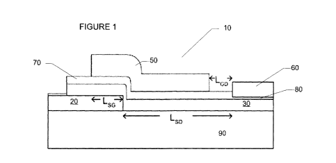
[0014] Figure 1 is a cross-sectional view of an embodiment of a top-gated ZnO
TFT with a
buried Schottky source barrier according to the invention.
[0015] Figure 2a is a confocal microscope image of an embodiment of a top-
gated TFT with a
buried Schottky source barrier according to the invention.
- 4 -
CA 02932446 2016-06-02
WO 2015/081416 PCT/CA2014/000863
[0016] Figure 2b is a graph showing output characteristics of an embodiment of
a ZnO SGTFT
according to the invention.
[0017] Figure 3 is a graph showing the transfer characteristics of an
embodiment of a ZnO
SGTFT according to the invention at a drain voltage of 10 V.
Detailed Description of the Invention
[0018] A detailed description of one or more embodiments of the invention is
provided below
along with accompanying figures that illustrate the principles of the
invention. The invention
is described in connection with such embodiments, but the invention is not
limited to any
embodiment. The scope of the invention is limited only by the claims and the
invention
encompasses numerous alternatives, modifications and equivalents. Numerous
specific
details are set forth in the following description in order to provide a
thorough understanding
of the invention. These details are provided for the purpose of example and
the invention
may be practiced according to the claims without some or all of these specific
details. For the
purpose of clarity, technical material that is known in the technical fields
related to the
invention has not been described in detail so that the invention is not
unnecessarily obscured.
[0019] The term "invention" and the like mean "the one or more inventions
disclosed in this
application", unless expressly specified otherwise.
[0020] The terms "an aspect", "an embodiment", "embodiment", "embodiments",
"the
embodiment", "the embodiments", "one or more embodiments", "some embodiments",
"certain embodiments", "one embodiment", "another embodiment" and the like
mean "one or
more (but not all) embodiments of the disclosed invention(s)", unless
expressly specified
otherwise.
[0021] The term "variation" of an invention means an embodiment of the
invention, unless
expressly specified otherwise.
[0022] A reference to "another embodiment" or "another aspect" in describing
an embodiment
does not imply that the referenced embodiment is mutually exclusive with
another
- 5 -
CA 02932446 2016-06-02
WO 2015/081416 PCT/CA2014/000863
embodiment (e.g., an embodiment described before the referenced embodiment),
unless
expressly specified otherwise.
[0023] The terms "including", "comprising" and variations thereof mean
"including but not
limited to", unless expressly specified otherwise.
[0024] The terms "a", "an" and "the" mean "one or more", unless expressly
specified otherwise.
The term "plurality" means "two or more", unless expressly specified
otherwise. The term
"herein" means "in the present application, including anything which may be
incorporated by
reference", unless expressly specified otherwise.
[0025] The term "e.g." and like terms mean "for example", and thus does not
limit the term or
phrase it explains.
[0026] The term "respective" and like terms mean "taken individually". Thus if
two or more
things have "respective" characteristics, then each such thing has its own
characteristic, and
these characteristics can be different from each other but need not be. For
example, the
phrase "each of two machines has a respective function" means that the first
such machine
has a function and the second such machine has a function as well. The
function of the first
machine may or may not be the same as the function of the second machine.
[0027] Where two or more terms or phrases are synonymous (e.g., because of an
explicit
statement that the terms or phrases are synonymous), instances of one such
term/phrase does
not mean instances of another such term/phrase must have a different meaning.
For example,
where a statement renders the meaning of "including" to be synonymous with
"including but
not limited to", the mere usage of the phrase "including but not limited to"
does not mean that
the term "including" means something other than "including but not limited
to".
[0028] Neither the Title (set forth at the beginning of the first page of the
present application)
nor the Abstract (set forth at the end of the present application) is to be
taken as limiting in
any way as the scope of the disclosed invention(s). An Abstract has been
included in this
application merely because an Abstract of not more than 150 words is required
under 37
C.F.R. Section 1.72(b) or similar law in other jurisdictions. The title of the
present
- 6 -
CA 02932446 2016-06-02
WO 2015/081416 PCT/CA2014/000863
application and headings of sections provided in the present application are
for convenience
only, and are not to be taken as limiting the disclosure in any way.
[0029] Numerous embodiments are described in the present application, and are
presented for
illustrative purposes only. The described embodiments are not, and are not
intended to be,
limiting in any sense. The presently disclosed invention(s) are widely
applicable to numerous
embodiments, as is readily apparent from the disclosure. One of ordinary skill
in the art will
recognize that the disclosed invention(s) may be practiced with various
modifications and
alterations, such as structural and logical modifications. Although particular
features of the
disclosed invention(s) may be described with reference to one or more
particular
embodiments and/or drawings, it should be understood that such features are
not limited to
usage in the one or more particular embodiments or drawings with reference to
which they
are described, unless expressly specified otherwise.
[0030] No embodiment of method steps or product elements described in the
present application
constitutes the invention claimed herein, or is essential to the invention
claimed herein, or is
coextensive with the invention claimed herein, except where it is either
expressly stated to be
so in this specification or expressly recited in a claim.
[0031] The top-gate SGTFT 10 (also referred to as "device") according to the
invention, as
shown in Fig. 1, includes a buried Schottky source barrier contact 20 which
functions as an
electrode. Unlike conventional TFTs fabricated using ohmic source/drain
contacts, the
depletion region from the Schottky junction at the source is responsible for
controlling the
current flow in the device rather than the channel conductance. For instance,
in the
conventional TFT, saturation occurs when the drain region is depleted of
carriers; whereas in
the SGTFT, saturation occurs when the semiconductor at the source is fully
depleted from
the Schottky barrier. As in the conventional ZnO TFT though, the SGTFT
operates as a
single carrier/unipolar n-channel transistor due to the intrinsic n-type
behaviour of ZnO,
which is unintentionally present in all types of deposition techniques.
[0032] Advantages of the SGTFT include a lower saturation voltage, higher
output impedance,
faster operating speeds (due to reduced minority carrier storage), and a
reduction in short-
channel effects. Conversely, the drive current of device 10 is noticeably
reduced compared
- 7 -
CA 02932446 2016-06-02
WO 2015/081416 PCT/CA2014/000863
to a conventional TFT due to the impedance of the Schottky barrier. Buried
source contact
20 is used to ensure that the interface between the Schottky metal and active
channel 30 layer
is protected from contaminants during other processing steps, making it easier
to control the
variables during the Schottky junction formation.
[0033] To relax the alignment constraints of the photolithography processes,
gate 50 may have a
top drain contact 60 rather than a buried contact under the active channel 30
layer like source
contact 20; this allows gate 50 and drain contact 60 to be fabricated at the
same time. As a
result, no alignment between the distance from drain contact 60 and gate 50 is
predefined
therefore ensuring more consistent breakdown voltages between devices. This
top gate
design also allows for easy integration with traditional circuits. Another
aspect of device 10
is the extremely thin, for example less than 5nm, high- lc gate oxide 70,
which is possible
using the ALD technique. This leads to enormous, for example, greater than
1MV/cm
electric fields in channel 30 consequently increasing device performance and
reducing
operating voltages. A ZnO SGTFT 10 with characteristics such as high drive
currents and
low operating voltages can be fabricated at low processing temperatures (less
than 150 C).
[0034] In the fabrication of the ZnO SGTFT 10, due to the low processing
temperatures, the
device can be patterned using photolithography and lift-off processes. Devices
10 can be
built on a clean, highly doped (z1016 cm3) p-type silicon (Si) wafer covered
with 50 nm
thick thermal silicon oxide (Si02). The SGTFT architecture is applicable with
nearly any
kind of insulating substrate 90, which includes flexible or plastic materials
if low temperature
deposition processes such as those disclosed herein are used. Using this
process, titanium
tungsten (TiW) (12 nm thick) is first sputtered and patterned using a lift-off
process to form
the source Schottky metal source contact 20. TiW is a stable alloy that is
resistant to acid
etches and oxidation. Other materials, such as Platinum, Gold, Copper,
Ruthenium, Silver,
or Tungsten, that can form a Schottky barrier with ZnO are also compatible
with the device
architecture as the source contact electrode 20.
[0035] After forming source contact 20, ZnO may be blanket deposited by the
ALD method (for
example, using a Kurt J. Lesker Company ALD-150LX system) using a thermal or
plasma
enhanced ALD process at 130 C. The precursors used for the ZnO deposition may
be
- 8 -
CA 02932446 2016-06-02
WO 2015/081416 PCT/CA2014/000863
Schottky metals on ZnO. Regardless of poorer Schottky barrier properties
though, using
TiW as the source barrier metal is attractive due to its relatively low cost
and robustness. In
the saturation regime, there is high series resistance being exhibited as seen
by the noticeable
positive slope in the family of curves. This is most likely the result of the
high carrier
concentration in the channel along with the non-ideal source Schottky barrier.
[0041] The transfer characteristics Ups vs. VGs) of the ZnO SGTFT at a drain
voltage of 10 V
are shown in Fig. 3. The method of extracting the threshold voltage (VTH) from
the linear
portion of (IE6)1/2 vs. VGs is also shown. From fitting a straight line to the
square root of IDS
versus VGs (also shown in Fig. 3), the threshold voltage (VTH) was extracted
to be 1.1 V.
The maximum current on/off ratio (IGN/IGFF) reaches 107, and the off-current
reaches low
values of approximately lx10-12 A at a pinch-off voltage of -1 V. Although the
pinch-off
voltage is negative, device 10 can nonetheless operate as an enhancement-mode
transistor
due to the positive VTH and the relatively low current at zero gate bias
1.5x10⁻⁸ A)
compared to the on-current values (greater than 1x10⁻⁵ A).
[0042] Carriers in SGTFT 10 are controlled by the gated field at the source,
so the turn-on
conditions for SGTFT 10 are less dependent on the properties of active channel
30.
Particularly, process variables such as the thickness and carrier
concentration of channel 30
have a lesser effect on Vth compared to the conventional TFT. This also
implies that the Vth
of the SGTFT is mostly determined by the properties of the source Schottky
barrier (e.g.
barrier height), which is advantageous for improving the fault tolerance of
fabricating
enhancement-mode devices. From fitting the linear portion of the transfer
curve, the field-
effect mobility (.1,FE) of the transistor was extracted to be 0.7 cm2 V-1 s-1
using Eq. (1)
(which applies when device 10 is in the saturation region):
[ WPFECox
l ( V GS Il th ) 5 s 2 ( DS V
DS = V
DS,sai) (1)
2 L SD
where C.õ is the gate oxide capacitance per unit area. The extracted channel
mobility is
within the same order of magnitude as other reported ALD ZnO TFTs that used
low
temperature processes. Therefore, the electrical performance of the SGTFT is
comparable
with other ALD ZnO TFTs that used conventional TFT architectures. The
subthreshold
-11-
CA 02932446 2016-06-02
WO 2015/081416 PCT/CA2014/000863
[0038] Following the photolithography for the gate oxide patterns, more
cycles, for example
another 50 cycles, of Hf02 are deposited. In the experiment this led to an
approximately 10
nm, or within a range of 3 to 20 nm, thick Hf02 film for the gate oxide 70
dielectric layer
(including Hf02 cap oxide layer 80) as measured from ellipsometry. Besides
Hf02, any
other insulating material (e.g. Zr02 or spin-on-dielectrics) that can be
deposited as a thin film
is suitable for use as the gate oxide 70 (the gate dielectric layer) in device
10. Lastly, an
ohmic metal is deposited and patterned with lift-off to form top gate 50 and
drain contact 60
electrodes. An Aluminum/gold (Al/Au) stack (of a large range, including 20
nm/60 nm) can
be used without any post-deposition annealing as the ohmic contacts.
Alternatively, different
metals can be used so long as they secure to ZnO and Hf02. A schematic of
device 10 is
shown in Fig. 1, and a confocal microscope image of a typical device is shown
in the inset in
Fig. 2a. In Fig. 2b, as shown in the graph, VGs is at 3.6 V for the top curve
and decreases in -
0.2 V increments until pinch-off. Using Hall Effect measurements, the electron
concentration of the ALD ZnO is on the order of 1017 cm-3. The measurements of
LSWW,
LsG, and LGD indicated in Figure 2b are typical, but are scalable downwards by
a factor of
100 and upwards by a factor of 10.
[0039] The output characteristics (drain current (IDs) vs. drain voltage
(VDs)) of a typical ZnO
SGTFT 10 with a buried TiW source Schottky contact 20 (measured using the
Keithley
Instruments Inc. 4200 semiconductor characterization system) is shown in Fig.
2b. The
dimensions of the device 10 are also given in the figure. Similar to other ZnO
TFTs that
utilized high- lc k dielectrics, there is high transconductance over a low
operating voltage
range. Also, n-channel behaviour is present as current density increased as
VGs was
increased. The device 10 in Fig. 2b also showed good drive current, reaching
120 A at a
gate voltage (VGS) of 3.6 V, despite the low temperature of the ALD ZnO
growth.
[0040] The saturation voltages in device 10 are much lower than prior devices
that did not use
the source Schottky barrier; however, they can be made even lower with a
higher quality
Schottky junction. From current-voltage (IV) measurements of Schottky diodes
formed from
TiW contacts on the ALD ZnO, an experiment measured a current on/off ratio of
10 and an
ideality factor of greater than 2 using thermionic emission theory. These
results are
characteristic of a highly non-ideal Schottky barrier and are poor compared to
other-known
-10-
CA 02932446 2016-06-02
WO 2015/081416 PCT/CA2014/000863
diethylzinc (DEZ) and water. ZnO films are grown with a thickness of
approximately 15 nm,
or in the range of 5 to 50 nm, which can be monitored in-situ utilizing a J.
A. Woollam Co.
Inc. M-2000D1 spectroscopic ellipsometer. The ZnO growth for device 10 is not
limited to
the ALD method; any thin film deposition technique for ZnO such as sol-gel,
pulsed laser
deposition (PLD), and radio frequency (rf) sputtering can also be used (a low
temperature
growth should be used for compatibility with flexible substrates). If the
thickness of the
source metal is kept below 15 nm, conformal thin film deposition techniques
such as PLD
can be used for the ZnO growth. Likewise, the device may include other
materials, as any
semiconducting material that can be deposited as a thin film at thicknesses
less than 25 nm is
suitable for use as active channel 30 (providing an appropriate Schottky metal
is used for
source contact 20).
[0036] Following the ZnO deposition, the ZnO may be etched using ferric
chloride (FeCl3) to
pattern channel 30 and form electrical isolation between devices 10 as needed.
Other wet or
dry etch processes for ZnO can be substituted for the FeCl3. The dimensions of
the channel
width (W) and length (LSD), the source-to-gate overlap (LsG) and gate-to-drain
distance (LGD)
of the devices 10 may be varied. Increasing LsG leads to higher output current
due to
increased lowering of the effective source barrier while LGD affects the
device breakdown
voltage. In an experiment, hafnium dioxide (Hf02) was blanket deposited by
plasma-
enhanced ALD at 100 C following a brief remote oxygen plasma (ROP) clean for
use as the
high-k gate insulator layer. Both the channel and gate dielectric films are
compatible with
inexpensive plastic or polymer-based substrates due to the low growth
temperatures of the
process.
[0037] The Hf02 deposition may be done using tetrakis(dimethylamino)hafnium
(TDMAHf) as
a precursor with ROP. Additionally, as a result of the low growth temperature,
the gate
oxide can be patterned using a lift-off process. In an experiment, a 10 cycle
1.7 nm thick)
Hf02 cap oxide layer 80 was first deposited after etching the ZnO (and before
photolithography) to protect the thin ZnO film from the photoresist developer,
which was
seen to etch ZnO. The only noticeable negative effect of using the Hf02 cap
oxide layer 80
is increasing the contact resistance; neglecting the cap oxide layer is not
detrimental to the
device performance.
- 9 -
CA 02932446 2016-06-02
WO 2015/081416 PCT/CA2014/000863
swing (SS), which is defined by Eq. (2), was extracted to be 192 mV/decade at
the maximum
slope in the transfer curve:
OV
SS ¨ GS (2)
a logio (/Ds
[0043] Compared to most ZnO TFTs, the SS of device 10 is among the lowest.
This is due to
the 10 nm thick high- lc k gate oxide, which is the thinnest gate oxide
reported for ZnO TFTs.
The thin gate oxide helps reduce fabrication costs, due to a shorter
deposition time, while
also allowing for higher electric fields in channel 30 leading to higher
transconductance and
better charge control. Measurements of the gate leakage current did not show
any
breakdown phenomena until VGs surpassed 5 V. When breakdown did occur, the
characteristics of the leakage current resembled that of Fowler-Nordheim
tunneling.
Consequently, these measurements indicate that the ALD-grown Hf02 is high
quality gate
oxide. Based on the above results, despite the relatively high carrier
concentration of the ZnO
channel deposited by ALD at 130 C, experiments were able to fabricate a ZnO
transistor
with good electrical characteristics that is suitable for flexible electronics
applications by
using a distinctive buried source Schottky barrier and top gate SGTFT
structure.
[0044] The above-described embodiments have been provided as examples, for
clarity in
understanding the invention. A person with skill in the art will recognize
that alterations,
modifications and variations may be effected to the embodiments described
above while
remaining within the scope of the invention as defined by claims appended
hereto.
- 12 -