Note: Descriptions are shown in the official language in which they were submitted.
CA 02932913 2016-06-06
WO 2015/069953
PCT/US2014/064437
PROTECTIVE COVERING FOR WEARABLE DEVICES
FIELD
These present application relates generally to personal electronics, portable
electronics,
wearable electronics, and more specifically to systems, electronics,
structures and methods for
wearable devices.
BACKGROUND
Electronic and structural systems used in wearable devices ought to be
designed to
withstand the rigors of use and repeated cycles of bending, flexing, strapping
on, un-strapping; as
well as environmental conditions such as temperature, humidity, moisture,
sweat, shock, and
vibration, just to name a few. Typically, processes and materials used in the
manufacture of a
wearable device may include the use of glue or adhesives to secure and/or
protect internal
components of the wearable device. Additionally, solder may be used to
electrically couple
wires or other components (e.g., surface mount devices) of the wearable
device. In that a
wearable device may be configured to be flexible for user by its users,
designing flexibility in the
wearable devices may require the use of flexible structures such as flexible
circuit boards and
other flexible materials that may be selected to retain a shape when the
wearable device is flexed
into a specific configurations, such as being flexed to wrap around a portion
of a user's body
(e.g., wrist, arm, ankle, leg, neck, head, etc.). However, the repeated
flexing of the wearable
device may lead to failure modes such as electrical shorts or opens in wires,
solder joints, traces
in the flexible circuit board, infiltration of glue, adhesives, or the like
into components such as
batteries or other electrical or electrical/mechanical components, just to
name a few. Moreover,
application of glue, adhesives, or the like may require manual trimming of
excess material after
it has dried or otherwise cured, leading to increased labor cost and
manufacturing time. In some
applications one or more covers or moldings may be applied to a wearable
device to cover and
protect already fabricated inner portions of the wearable device. Components
of the inner
portions may need to be covered or otherwise protected from subsequent molding
operations that
may result in damage to those components due to heat and/or infiltration of
the molding material,
for example. Components positioned at locations within the wearable device
that will be
subjected to forces from flexing may eventually fail due to constrained
movement when the
wearable device is flexed. For examples, wires or electrical traces may fail
if they are not free to
flex as the wearable device is flexed. Restricted movement of the wires/traces
may lead to
broken solder joints, breakage, shorts, or intermittent continuity.
1
CA 02932913 2016-06-06
WO 2015/069953
PCT/US2014/064437
Accordingly, there is a need for systems, electronics, structures and methods
for
fabrication of wearable devices that enable reliable manufacture and operation
of wearable
devices.
BRIEF DESCRIPTION OF THE DRAWINGS
Various embodiments or examples ("examples") of the present application are
disclosed
in the following detailed description and the accompanying drawings. The
drawings are not
necessarily to scale:
FIGS. lA ¨ 1B depict a cross-sectional view of a flexible substrate including
a first
relaxation structure and a flexible dielectric including a second relaxation
structure, according to
an embodiment of the present application;
FIGS. 1C ¨ 1D depict cross-sectional views of a flexible substrate and
flexible dielectric
that include a plurality of first relaxation structures and second relaxation
structures, according to
an embodiment of the present application;
FIG. 2A depicts a top plan view of a flexible dielectric and associated
structures,
according to an embodiment of the present application;
FIG. 2B depicts a cross-sectional view of a flexible dielectric, according to
an
embodiment of the present application;
FIG. 3A depicts a top plan view of a flexible dielectric and examples of
associated
structures, according to an embodiment of the present application;
FIG. 3B depicts a cross-sectional view of a flexible dielectric and examples
of associated
structures, according to an embodiment of the present application;
FIGS. 3C ¨ 3D depict top plan views of a flexible dielectric and associated
structures,
according to an embodiment of the present application;
FIGS. 4A ¨ 4B depict top plan views of a flexible dielectric and associated
structures,
according to an embodiment of the present application;
FIGS. 5A ¨ 5E depict cross-sectional views of a flexible substrate, a flexible
dielectric,
and associated structures, according to an embodiment of the present
application;
FIG. 6A depicts one example of a mandrel, according to an embodiment of the
present
application;
FIGS. 6B ¨ 6G depict examples of different configurations for a mandrel,
according to an
embodiment of the present application;
FIG. 7A depicts a cross-sectional view of one example of a flexible and
electrically non-
conductive cover, according to an embodiment of the present application;
2
CA 02932913 2016-06-06
WO 2015/069953
PCT/US2014/064437
FIG. 7B depicts one example of a flexible and electrically non-conductive
cover after
shrinking in a dimension, according to an embodiment of the present
application;
FIG. 8A depicts a cross-sectional view of another example of a flexible and
electrically
non-conductive cover, according to an embodiment of the present application;
FIG. 8B depicts a cross-sectional view of one example of a plurality of
sections of a
flexible and electrically non-conductive cover, according to an embodiment of
the present
application;
FIGS. 9A ¨ 9C depict cross-sectional views of examples of alternative
configurations for
a relaxation structure connected with a flexible substrate, according to an
embodiment of the
present application;
FIG. 10A depicts a profile view of one example of a partially assembled
wearable device,
according to an embodiment of the present application;
FIG. 10B depicts a cross-sectional view of one example of a partially
assembled
wearable device, according to an embodiment of the present application;
FIGS. 10C depicts a cross-sectional view of one example of a partially
assembled
wearable device including a flexible substrate, a flexible dielectric, and a
plurality of flexure
points, according to an embodiment of the present application;
FIGS. 10D depicts a cross-sectional view of one example of the configuration
depicted in
FIG. 10C at a subsequent stage of fabrication, according to an embodiment of
the present
application;
FIG. 11 depicts a profile view of one example of a partially assembled
wearable device
including a flexible and electrically non-conductive cover after a shrinking
process, according to
an embodiment of the present application;
FIG. 12 depicts a profile view of one example of a flexible overmolding,
according to an
embodiment of the present application;
FIG. 13 depicts views of different examples of wearable devices configured to
be flexibly
worn on a structure, according to an embodiment of the present application;
FIG. 14 depicts a cross-sectional view of a wearable device flexibly mounted
to a portion
of a structure, according to an embodiment of the present application; and
FIG. 15 depicts one example of a flow diagram for a method for fabricating a
wearable
device, according to an embodiment of the present application.
DETAILED DESCRIPTION
3
CA 02932913 2016-06-06
WO 2015/069953
PCT/US2014/064437
Various embodiments or examples may be implemented in numerous ways, including
as
a system, a process, an apparatus, a user interface, or a series of program
instructions on a non-
transitory computer readable medium such as a computer readable storage medium
or a
computer network where the program instructions are sent over optical,
electronic, or wireless
communication links. In general, operations of disclosed processes may be
performed in an
arbitrary order, unless otherwise provided in the claims.
A detailed description of one or more examples is provided below along with
accompanying drawing FIGS. The detailed description is provided in connection
with such
examples, but is not limited to any particular example. The scope is limited
only by the claims
and numerous alternatives, modifications, and equivalents are encompassed.
Numerous specific
details are set forth in the following description in order to provide a
thorough understanding.
These details are provided for the purpose of example and the described
techniques may be
practiced according to the claims without some or all of these specific
details. For clarity,
technical material that is known in the technical fields related to the
examples has not been
described in detail to avoid unnecessarily obscuring the description.
FIGS. lA ¨ 1B depict a cross-sectional view of a flexible substrate 110
including a first
relaxation structure 111 and a flexible dielectric 120 including a second
relaxation structure 122.
The first and second relaxation structures (111, 122) may be positioned
relative to each other for
form a flexure point 150 in a wearable device 100. Here, a finished wearable
device 100 is not
depicted and subsequent FIGS. will depict the wearable device 100 at different
stages of
fabrication leading up to a manufactured (e.g., finished) wearable device 100.
Wearable device
100 may include a plurality of flexure points 150 that are defined by
pluralities of first and
second relaxation structures (111, 122). Components may be positioned on one
or both sides
(151, 152) of the flexure point 150 and those components may be positioned on
surfaces 110s
and/or 120s of the substrate 110 and dielectric 120. Substrate 110 and
dielectric 120 may be
mechanically coupled with each other to prevent relative motion between the
substrate 110 and
dielectric 120 at one or more locations. For example, surfaces 115 and 126 may
be connected or
otherwise mechanically coupled with each other using a variety of techniques
including but not
limited to gluing, fastening (e.g., using a fastener), stapling, adhesive
bonding, welding, friction
stir welding, ultrasonic welding, clamping, and crimping, just to name a few.
As one example,
glue or an adhesive material may be applied between an interface 129 between
surfaces 115 and
126 and allowed to cure to couple the substrate 110 with the dielectric 120.
The relative
positioning of the first and second relaxation structures (111, 122) may
define a space 104
4
CA 02932913 2016-06-06
WO 2015/069953
PCT/US2014/064437
between the relaxation structures (111, 122) having a shape that may be
determined in part by
shapes and/or contours of the relaxation structures (111, 122). In some
applications a structure
such as a mandrel (not shown), for example, may be positioned in the space 104
as will be
described below.
In FIG. 1B, the first and second relaxation structures (111, 122) allow for
flexing 102
(e.g., flexure, bending, curving, twisting, being bent or curved, etc.) of the
substrate 110 and
dielectric 120 proximate the flexure point 150 in response to one or more
forces Fl ¨ F4 are
applied to the wearable device 100, such as forces required to flex or bend
the wearable device
100 into a configuration for use by a user of the wearable device 100. An
example of a
configuration may include flexure caused by wrapping or un-wrapping the
wearable device 100
from a wrist, ankle, neck, torso, or other portion of a body or structure. The
user may not be a
human being and in some applications the wearable device 100 may be worn by an
inanimate
structure (e.g., a post). Although the first and second relaxation structures
(111, 122) are
depicted as having a curved or arcuate shape or profile, the present
application is not limited to
the shapes and/or profiles depicted. Moreover, the first and second relaxation
structures (111,
122) need not have the same shape and/or profile. A span 113 and 124 (e.g., a
distance across
from 151 to 152) for the first and second relaxation structures (111, 122)
respectively may be the
same or different. A relative position between the first and second relaxation
structures (111,
122) may not be symmetric. Using X-Y-Z axes 155 as a reference point for
purposes of
explanation, first and second relaxation structures (111, 122) may be
symmetrically positioned
relative to each other or may be positioned in displaced relationship relative
to each other. For
example, a displaced positioning may comprise second relaxation structure 122
being shifted to
the left or to the right on the X-axis relative to the first relaxation
structure 111. As another
example, the displaced positioning may comprise the first relaxation structure
111 may be
shifted into or out of the drawing sheet along the Y-axis relative to the
second relaxation
structure 122. Along the Z-axis, a height (h2, hl) of the first and second
relaxation structures
(111, 122) (e.g., as measured from an origin 0) may be the same or different.
FIGS. 1C ¨ 1D depict cross-sectional views of flexible substrate 110 and
flexible
dielectric 120 including a plurality of first relaxation structures and second
relaxation structures
that define a plurality of flexure points denoted as 150a ¨ 150d in FIG. 1C
and 150e ¨ 150k in
FIG. 1D. In FIG. 1C the first and second relaxation structures (111, 122)
include arcuate profiles
(e.g., curved, oval-shaped, or semicircular shaped); whereas, in FIG. 1C the
first and second
relaxation structures (111, 122) include angular profiles (e.g., triangular or
sloped). Actual
5
CA 02932913 2016-06-06
WO 2015/069953
PCT/US2014/064437
profiles, shapes and dimensions will be application dependent and are not
limited to the
examples described herein. As will be described below, one or more flexure
points, such as
those depicted in FIGS. 1C ¨ 1D may be positioned at predetermined locations
in wearable
device 100 to accommodate flexing of the wearable device 100 and/or to prevent
damage to
components (e.g., wiring, conductive traces, or structure) of the wearable
device 100 that may
be caused by flexing. In FIGS. 1C ¨ 1D (see also FIGS. 8A ¨ 8B and 10C ¨ 10D)
the wearable
device 100 may have an overall length L configured to accommodate mounting the
device 100
on a selected portion of a user's body (e.g., the arms, the legs, the neck,
the chest, the head, the
abdomen, etc.). For example, to fit around the circumference or perimeter of a
wrist or ankle,
length L may be a first length and have M flexure points 150; whereas, for
larger portions of a
body such as a circumference or perimeter of a torso, neck, thigh, head, calf
or bicep, length L
may be a second length that is longer than the first length and have N flexure
points 150, where
N may be larger than M.
Moving now to FIG. 2A where a top plan view of the flexible dielectric 120 and
associated structures are depicted. Flexible dielectric 120 may include one or
more structures
including but not limited to electrically conductive traces, wire(s), bonding
pads, strain reliefs,
vias, throughs, electrical components, mechanical components, electro-
mechanical components,
MEMS components, power supplies (e.g., a battery), vibration motors/engines,
gyroscopes,
accelerometers, microphones, speakers, indicator lights (e.g., LED's),
switches/buttons, just to
name a few. In FIG. 2A, a plurality of electrically conductive traces 201 are
depicted, but there
may be more or fewer traces 201. Traces 201 may be positioned on a surface
120s or other
position on dielectric 120. Traces 201 may be made from and electrically
conductive material
including but not limited to metal, metal alloys, electrically conductive
inks, dyes, paste,
nanotubes, just to name a few.
In FIG. 2B, a cross-sectional view of dielectric 120 along dashed line AA-AA
of FIG. 2B
depicts examples of structures that may be included in dielectric 120. Surface
120s may include
one or traces 201 and one or more electrically conductive nodes 250 (e.g.,
bonding pads). A
surface 250s of nodes 250 may be configured to receive another electrically
conductive structure,
such as a wire, solder, or both, for example. Another surface 126 may include
traces 201. An
interior of dielectric 120 may also include one or more traces 201 and may
include one or more
vias 203 for electrically coupling structures such as traces 201 and nodes
250. Dielectric 120
may have a thickness t that is application dependent. For example, thickness t
may be about
2mm or less. Flexible dielectric (FD) 120 may comprises a material including
but not limited to
6
CA 02932913 2016-06-06
WO 2015/069953
PCT/US2014/064437
flexible printed circuitry (FPC), flat flexible cable (FFC), a flexible
circuit board, and other
forms of flexible substrates made from a dielectric material and optionally
include structures
such as electrically conductive structures, just to name a few.
FIGS. 3A and 3B depict top plan and cross-sectional views respectively of FD
120 and
examples of associated structures that may optionally be included with FD 120.
FD 120 may
include one or more of nodes 250, traces 201, and components 310 ¨ 340.
Components 310 ¨
340 may be electrically coupled with traces 201 via soldering (e.g., surface
mount) or other
processes. One or more of traces 201 may be electrically coupled with nodes
250 and the nodes
250 may be electrically coupled with other structures such as wires and/or
solder bumps or the
like. Associated structures may be positioned on surface 120s.
In FIG. 3B, the cross-sectional view depicts an example where nodes 250 have
wire ends
383 of wires 381 electrically coupled with the nodes 250 using solder 385.
Moreover, an
encapsulating structure 380 (e.g., made from an electrically non-conductive
material) may be
formed on FD 120 and may partially or completely surround one or more
structures such as
nodes 250, solder 385, wire ends 383 and a portion of wires 381. Wires 318 may
be insulated
wires or may be un-insulated wires. Encapsulating structure 380 may be
configured to protect
the structures it encapsulates, to provide mechanical stability and/or
isolation, to provide strain
relief, protect against moisture and/or corrosion that may be caused by
chemicals, fluids, or the
like, or to protect the encapsulated structures from subsequent fabrication
steps, just to name a
few. In some applications, one or both sides (151, 152) of flexure point 150
may include the
associated structure depicted in FIGS. 3A and/or 3B.
FIGS. 3C and 3D depict top plan views of FD 120 and additional examples of
associated
structures that may be optionally included with FD 120. In FIGS. 3C and 3D,
second relaxation
region 122 is denoted in dashed lines and associated components that may be
included with FD
120 are depicted on both sides (151, 152) of flexure point 150, although in
other examples the
associated components may be positioned on only one of the sides (151, 152).
Referring now to
FIG. 3C, a span 390 across second relaxation region 122 is straddled by wires
381 which
terminate at nodes 250 and 250a in encapsulating structures 380 and 380a. As
will be described
below, wires 381 may have a contour, profile or shape (e.g., arcuate shape)
across span 390 that
approximately matches a contour, profile or shape of the second relaxation
structure 122. Wires
381 or other electrically conductive structures may be pre-shaped to include
the contour, profile
or shape, be bent or otherwise mechanically manipulated to have the contour,
profile or shape,
for example. In FIG. 3C wires 381 and nodes 250 are depicted as being
approximately aligned
7
CA 02932913 2016-06-06
WO 2015/069953
PCT/US2014/064437
with one another with wires 381 straddling span 390 in an approximately
straight line or linear
path. However, the wires 381, nodes 250 or other associated structures on FD
120 may not be so
configured and may not be aligned or laid out in straight lines.
In FIG. 3D, nodes 250 and 250a are not aligned with each other and wires 381
are
dressed across span 390 in a non-linear path and each wire 381 may include
bends or folds 382
along its length. Dressing wires 381 or other electrically conductive
structures that straddle the
second relaxation region 122 may be used for a variety of purposes including
but not limited to
preventing the wires from kinking or having sharp bends that may cause the
wire to fail due to
opens, or intermittent continuity, to set a profile in the wires as they
straddle the span 390, and to
create or relieve tension in the wires, just to name a few. In FIGS. 3C ¨ 3D,
the portion of FD
120 that forms the second relaxation region 122 may include electrically
conductive traces such
as those depicted 2A ¨ 3D (e.g., like traces 201) that may supplement or
replace wires 381. In
other applications the portion of FD 120 that forms the second relaxation
region 122 may not
include traces. Traces may be exclude from second relaxation region 122 to
prevent fatigue from
repeated flexing of the second relaxation region 122 from causing potential
mechanical failure of
the traces that could lead to intermittent continuity, open circuits or short
circuits, for example.
Turning now to FIGS. 4A ¨ 4B where top plan views of FD 120 and associated
structures includes a strain relief 400 that may be positioned on one or both
of the sides (151,
152). Strain relief 400 is in contact with a portion of one or more of the
wires 381 and may be
operative to restrain movement of the wires 381, prevent the wires 381 from
being stressed, or
prevent wire ends 383 from being pulled from their respective nodes 250 and/or
from becoming
unsoldered, for example. The strain relief 400 may be positioned between the
nodes 250 and/or
encapsulating structure 380 and the sides (151, 152) of the second relaxation
region 122.
In FIG. 4B, some of the wires 381 may not terminate at a node 250 and may
instead be
electrically coupled with a component 450 or other structure on either side
(151, 152) of the
second relaxation region 122. For example, component 450 on the second side
152 may be a
power source such as a battery and three of the wires 381 that straddle span
390 may be
electrically coupled with component 450 and another wire 381 may be
electrically coupled with
a node 250b in encapsulating structure 380b. Strain relief 400 and second side
152 may prevent
the wires 381 from being disconnected and/or dislodged from component 450 due
to flexing at
flexure point 150.
Reference is now made to FIGS. 5A ¨ 5E were cross-sectional views depict
flexible
substrate (FS) 110, FD 120 and associated structures including strain reliefs
400. In FIG. 5A,
8
CA 02932913 2016-06-06
WO 2015/069953
PCT/US2014/064437
wire 381 is depicted straddling span 390 and having portions of wire 381 in
contact (510, 520)
with strain reliefs 400 and both sides (151, 152) of second relaxation region
122. Ends (512,
522) of wire 381 may be electrically terminated in any manner including but
not limited to those
discussed above, such as soldering to nodes 250, crimping, splicing, etc.
Here, wire 381 may
have a profile 505 over its span 390 of the second relaxation region 122 and
that profile may or
may not approximately match a profile of the second relaxation region 122.
Optionally, FD 120
and FS 110 may include vias, thrus, or the like denoted here as 530 and a
structure such as a
wire, electrically conductive trace or other may be routed or otherwise
positioned in via 530. For
example, wires 507 and 509 may be routed between the FS 110 and FD 120 using
vias 530.
Optionally, another electrically conductive structure 511 (e.g., a wire) may
straddle span 390
over first relaxation structure 111 and may have a profile 525 over the span
390. Wire 511 may
be routed through one or more of the vias 530. A surface 110s of FD 110 may
include one or
more components 550 that may be electrically coupled with electrically
conductive structures
such as wire 511, wire 507, wire 381 or other and one or more of the vias 530
may be used to
route electrically conductive structures to the one or more components 550
mounted on surface
110s. For example, wire 507 may be electrically coupled with component 550 and
routed
through via 530 for electrical connection with a structure on FD 120, such as
wire 381.
Referring now to FIG. 5B, in some examples, a strain relief 500 may be
connected with a
component 560 and an end 521 of wire 381 may be electrically coupled with the
component and
connected 520 with the strain relief 500. Here, strain relief 500 is not
connected with FD 120. A
component mounted strain relief, such as 500, may be used to prevent strain on
wire 381 from
causing a wiring failure such as a short, open, or intermittent and/or prevent
the wire 381 from
being pulled out or otherwise dislodged from its electrical connection with
component 560.
Moving now to FIGS. 5C ¨ 5E, an alternative configuration may include a second
relaxation structure 522 positioned at flexure point 150 and includes
electrical connectors 553
and 557 disposed on first and second sides 151 and 152 respectively, and also
includes an
electrically conductive structure 581 that straddles span 390. FD 120 may
comprise separate
segments that are positioned on sides (151, 152) with each segment including a
connector 551
and 555 which are configured to mate or otherwise electrically and
mechanically couple with
connectors 553 and 557 to establish an electrical connection with electrically
conductive
structures 552 and 554 (e.g., wires or conductive traces) in FD 120.
Electrically conductive
structure 581 (wire 581 hereinafter) may be a wire, an electrically conductive
trace or other
structure. Wire 581 may have the profile 505 as described above. In some
examples, wire 581
9
CA 02932913 2016-06-06
WO 2015/069953
PCT/US2014/064437
may be positioned internal to second relaxation structure 522 (see FIG. 5C),
may be positioned
over second relaxation structure 522 (see FIG. 5D), or may be positioned under
second
relaxation structure 522 (see FIG. 5E). Other structures such as components,
strain reliefs,
nodes, bonding pads, vias, encapsulating structures are not depicted in FIGS.
5C ¨ 5E for
purposes of explanation; however, one or more of those structures may be
included with the
examples depicted in FIGS. 5C ¨ 5E. Connectors (551, 555, 557, 553) may be
male and female
and may be implemented using any suitable connector technology. Connectors
(551, 555, 557,
553) may include pins, terminals or other structures that allow an electrical
connection to be
made between electrically conductive structures in FD 120 and the connectors.
Connectors (551,
555, 557, 553) may include a wide variety of pitch and circuit sizes, may
include ZIF and Non-
ZIF actuators, and may include covers or other structures that allow for
secure connection
between terminals of the connectors and FD 120. Second relaxation structure
522, FD 120 or
both may be made from flexible printed circuitry (FPC), flat flexible cable
(FFC) or other type of
flexible substrates suitable for electronics, for example.
Attention is now directed to FIG. 6A where one example of a mandrel 600 is
depicted.
Mandrel 600 may be positioned in space 104 between the first and second
relaxation structures
111 and 122. A shape of mandrel 600 may be selected to set a profile 605 of
the second
relaxation structure 122. Mandrel 600 may be positioned in space 104 to
prevent second
relaxation structure 122 from collapsing and/or deforming into a contour or
profile that may
adversely affect operation of flexure point 150 when the wearable device 100
is flexed 102 (see
FIG. 1B). In some examples, one or more surfaces 600s of mandrel 600 may be in
contact,
permanently or intermittently, with surface 122s, surface 111s or both.
Mandrel 600 may be
made from a variety of materials including but not limited to metals, metal
alloys, plastics, foam,
wood, rubber, glass, composite materials, synthetic materials, Teflon or
equivalent materials, and
paper, just to name a few. Mandrel 600 may be configured to be deformable
(e.g., foam) or non-
deformable (e.g., metal). A plurality of the mandrels 600 may be used and
mandrel's 600 may
vary is dimensions and shape among a plurality of flexure points 150 (see
FIGS. 1C and 1D).
In FIGS. 6B ¨ 6G, non-limiting examples of different configurations for
mandrel 600 are
depicted. In FIG. 6B, mandrel 602 may be cylindrical as in a solid cylinder or
as in a cylindrical
tube, for example. In FIG. 6C, mandrel 601 may have an arcuate shape and a
surface 601b may
contact portions of surface 111s. In FIG. 6D, mandrel 613 may have triangular
shape and a
surface 613b may contact portions of surface 111s. Triangular shape for
mandrel 613 may be
used to set a profile of second relaxation structure 122 (e.g., 150e ¨ 150k of
FIG. 1D). In FIG.
CA 02932913 2016-06-06
WO 2015/069953
PCT/US2014/064437
6E, a composite mandrel may include portions 603 and 605 joined at surfaces
603s and 605s and
may have an overall circular or cylindrical shape. A surface 605b of portion
605 may contact
portions of surface 111s. In FIG. 6F, a composite mandrel may include portions
607 and 609
joined at surfaces 607s and 609s and may have an arcuate or conical shape for
portion 607 and a
semi-circular shape for portion 609. A surface 609b of portion 609 may contact
portions of
surface 111s. In FIG. 6G, mandrel 611 may have an ovoid shape and surface 611b
may contact
portions of surface 111s. Composite mandrels may have portions that are made
from different
materials. The mandrels depicted may include materials or be coated with a
material that
lubricates one or both of the relaxation structures (111, 122) and/or reduces
friction between
surfaces of the mandrel and one or both of the relaxation structures (111,
122).
FIG. 7A depicts a cross-sectional view of one example of a flexible and
electrically non-
conductive cover 700 (cover 700 hereinafter). FD 120, FS 110 and associated
structures carried
by FD 120 and FS 110 are positioned 730 in an interior 732 of cover 700. Cover
700 may
include a pre-shrink dimension Do that is large enough to accommodate
insertion of the
aforementioned structures (e.g., device 100). As will be described below,
cover 700 may
comprise a single section of material or a plurality of sections which may be
made from different
materials. Suitable flexible materials for the cover 700 and/or its plurality
of sections include but
are not limited to shrink tubing, heat shrink tubing, thin wall heat shrink
tubing, ultra-thin wall
heat shrink tubing, medical grade tubing, high temperature medical grade
tubing, Polyester
(PET) heat shrink tubing, Polyether tubing, heat shrinkable polyolefin tubing,
ultra-thin wall
Polyolefin heat shrink tubing, PBEAX heat shrink tubing, PEBA heat shrink
tubing,
Polyvinylidene Fluoride (PVDF) tubing, Silicone tubing, Polyethylene (PE)
tubing,
Polytetrafluorethylene (PTFE) tubing, Teflon tubing, fluoroelastomer tubing,
and the like, for
example. The medical grade tubing and/or high temperature medical grade tubing
may be
shrunk by applying heat (e.g., 710) as described herein. Material properties
for the cover 700
and/or it plurality of sections may include but are not limited to low
shrinkage in a longitudinal
direction (e.g., a direction Lo that is perpendicular to Do), conformal (e.g.,
conformally covering
as in FIG. 7B), surface finish, tough, tight fitting, durable, dimensional
stability (e.g., due to
heating during manufacturing and post manufacturing), stable, flexibility,
transparency to light,
and thin or ultra-thin wall thicknesses (e.g., WT), shrink ratio (e.g., in a
range from about 1.5:1 to
about 4.5:1), temperature stability (e.g., from about 100 C to about 265 C),
resistance to water
and/or moisture, just to name a few. For example, shrink ratios from about 2:1
minimum to
about 4:1 maximum may be desirable material properties along with a wall
thickness WT of
11
CA 02932913 2016-06-06
WO 2015/069953
PCT/US2014/064437
about 0.1mm and a temperature stability of the material at molding
temperatures for the
overmolding 1200. For example, if cover 700 has an inside diameter (ID) of
about 3/8" prior to
heat 710 being applied to cover 700, then after heating, the ID may shrink to
about 0.187 inches,
(e.g., about a 2:1 shrinkage ratio). Other examples may include a before
heating ID of about
1/2" and an after heating ID of about 1/4" or about 3/4" ID before and about
3/8" ID after. A
temperature at which the cover 700 and/or its plurality of sections shrink may
be about 90 C.
Operating temperatures for the cover 700 and/or its plurality of sections may
be in a range from
about -55 C to about 274 C. An actual size of the assembly that is inserted
730 within the
interior diameter Do will be application dependent, however a product size
from about 0.250" to
about 0.5" is one non-limiting example of dimensions of a work piece (e.g.,
100) or other
assembly to be covered by cover 700.
Here, FD 120 may include structures including but not limited to components
750 ¨ 754,
wire 381, nodes 250, encapsulating structure 380, and strain relief 400.
Although not depicted,
FS 110 may also include structures. Cover 700 may be transparent 740 to allow
for visual or
machine inspection for quality control or other manufacturing purpose.
Transparent 740 may
include optically transparent. In some applications a light sensor (e.g., PIN
Diode) or light
emitting component (e.g., LED) may be mounted to FD 120 and cover 700 being
transparent 740
may allow for light to be received or transmitted through cover 700. In some
examples, one or
more portions of cover 700 may be transparent 740.
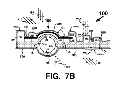
In FIG. 7B, after positioning 730 in the interior 732 (e.g., after Final
Assembly Test &
Packaging- FATP), heat 710 and/or some other process may be applied to the
cover 700 to
shrink cover 700 in one or more dimensions. Upon shrinking, cover 700 may
partially or
completely conformally cover 701 structures including but not limited to the
FS 110, FD 120,
and other structures carried by the FS 110 and FD 120, such as components 750
¨ 754, wire 381,
nodes 250, encapsulating structure 380, and strain relief 400. Cover 700 or
the one or more
sections of cover 700 may be made from a material that when heated 710 or
otherwise caused to
shrink, shrinks cover 700 or its one or more section in a dimension by a ratio
(e.g., of at least
about 1.5:1). For example, shrinkage of cover 700 in a ratio of about 2:1 to
about 4:1 may be
desirable for some applications. Actual ratios may be application dependent,
material dependent
or process dependent and are not limited by the examples herein. In some
examples, after
shrinking cover 700, or one or more of its sections, subsequent fabrication
steps may involve
high temperatures. Therefore, in some applications a material for cover 700,
or its one or more
sections, may be selected to be mechanically stable over a temperature range
from about 100 C
12
CA 02932913 2016-06-06
WO 2015/069953
PCT/US2014/064437
to about 300 C. Although heat 710 is depicted as one method for causing the
cover 700 to
shrink, the present application is not limited to heating 710 and other
processes or combinations
of processes may be used. For example, a composition of matter, such as a
chemical or solvent
may be applied to cover 700 to cause shrinking. In some examples, a vacuum may
be applied to
cover 700 (e.g., to evacuate air from interior 732) to cause cover to collapse
and/or shrink in a
dimension that conformally covers some or all of the structure described
above. After applying
the vacuum, heat, chemicals, a composition of matter or other may be applied
to cover to cause
additional shrinking, to set the shrinking that has already occurred, or to
cure the cover 700 to
cause the shrinking to set. In other examples, cover 700 may be irradiated by
one or more
wavelengths of light or other forms of electromagnetic radiation.
After shrinking, pre-shrink dimension Do may be reduced to a post-shrink
dimension DF.
Post-shrink dimension DF may vary based on the components or other structures
being covered
and/or conformally covered by the cover 700 as depicted in FIG. 7B. For
example, DF is greater
at conformal covering of component 750 than at conformal covering of component
754 or at
conformal covering of wire 381 on first side 151.
FIG. 8A depicts a cross-sectional view of cover 700 having FD 120 and FS 100
and their
respective flexure points 150a ¨ 150d positioned in its interior 732. For
purposes of explanation,
components and other structures that may be carried by FD 120 and FS 100 are
not depicted in
FIGS. 8A ¨ 8B. Cover 700 may subsequently be heated 710 or subjected to some
other process
to cause shrinking. In FIG. 8B, one example of a cover comprised of a
plurality of cover
sections is depicted. Here, cover sections 801, 803, 805, and 807 have a
portion of FD 120 and
FS 100 and their respective flexure points 150e ¨ 150k positioned in their
respective interiors
732. In some examples, one or more of the cover sections may overlap each
other as depicted by
dashed ovals 811, 813, and 815. In some examples, after shrinking the cover
sections (801, 803,
805, and 807) the overlap (811, 813, and 815) between some or all of the cover
sections (801,
803, 805, and 807) may be retained. Materials for one or more of the cover
sections (801, 803,
805, and 807) may be the same or different and one or more of the cover
sections (801, 803, 805,
and 807) may be transparent 740 as described above.
Pre-shrink dimension Do of one or more of the cover sections (801, 803, 805,
and 807)
may be the same or different. One or more of the cover sections (801, 803,
805, and 807) may
be selected to have a first pre-shrink dimension Do configured to accept
portions of FD 120 and
FS 100 and also be configured to fit within another cover section having a
second pre-shrink
dimension Do that is larger than the first pre-shrink dimension Do, such as
cover sections 801 and
13
CA 02932913 2016-06-06
WO 2015/069953
PCT/US2014/064437
803 fitting within cover section 805. Multiple cover sections may be shrunk
all at the same time
or in some sequenced order. For example, given cover sections (801, 803, 805,
and 807), cover
sections 801 and 803 may be positioned over their respective portions of FD
120 and FS 110 and
then have heat 710 or other process applied to shrink 801 and 803. Next, cover
section 805 may
be positioned and shrunk, followed by cover section 807 being positioned and
then shrunk.
Reference is now made to FIGS. 9A ¨ 9C where cross-sectional views depict
examples
900a ¨ 900c of alternative configurations for the first relaxation structure
denoted as 911. First
relaxation structure 911 may be positioned at flexure point 150 as describe
above. Portions 913
and 915 of first relaxation structure 911 may be configured to connect with FS
110. For
example, slots, grooves, apertures or the like in structure 911 may be
configured to receive a
portion of FS 110. Materials for the first relaxation structure 911 and the FS
110 may be the
same or different. Glue, adhesives, crimping, stamping, fasteners or the like
may be used to
connect (913, 915) 911 and FS 110 to one another. First relaxation structure
911 may be
configured to allow flexing 902 in a manner similar to or identical to flexing
102 as described
above. First relaxation structure 911 may be used instead of an integrally
formed first relaxation
structure 111 as described above. First relaxation structure 911 may be
selected for application
specific properties and/or materials. FS 110 may be made from a first material
(e.g., a metal or
metal allow) and first relaxation structure 911 may be made from a second
material (e.g., rubber
or an elastomer) that is different than the first material. First relaxation
structure 911 may be
selected for properties including but not limited to durability, number of
flexure 902 cycles,
resistance to heat or other processing environments, and specific flexing
properties, just to name
a few.
FIG. 9B depicts another configuration 900b where first relaxation structure
911 may
include arcuate surfaces as denoted in dashed ovals 977 that may be used to
provide a smooth
and/or conformal surface for FD 120 which may be connected with one or more
portions of first
relaxation structure 911. FIG. 9B also depicts an example of how the first and
second relaxation
structures (911, 122) operate to impart flexing 902 at flexure point 150. FIG.
9C depicts yet
another configuration 900c where FS 110 includes portions 925 including a
shape configured to
connect (913, 915) and retain FS 110 in first relaxation structure 911.
Turning now to FIGS. 10A ¨ 10B, where profile and cross-sectional views
respectively,
depict one example of a partially assembled wearable device 100. In FIGS. 10A
¨ 10B wearable
device 100 includes a plurality of components denoted as 1010 ¨ 1022 and 1011
¨ 1017. FS 110
and FD 120 include a plurality of flexure points denoted as 150a ¨ 150f. For
purposes of
14
CA 02932913 2016-06-06
WO 2015/069953
PCT/US2014/064437
explanation details such as the first and second relaxation structures (111
and/or 911, 122) are
not depicted in FIGS. 10A ¨ 10B. One or more of the flexure points 150 on
wearable device 100
may be positioned at locations that suit application specific needs or may be
customized for a
bespoke application. As one example, the plurality of flexure points 150a ¨
150f may be
selected to allow wearable device 100 to be flexibly worn about a body portion
1050 or some
other structure. Body portion 1050 may be a cross-sectional profile of a body
part such as a
wrist, arm, neck, leg, ankle or the like, for example. Component 1010 may be a
power source
such as a rechargeable power source (e.g., a Lithium Ion battery) and
component 1010 may be
rigid or un-flexible. Therefore, it may be a matter of design choice to place
flexure points 150c
and 150d on either side of component 1010 so that wearable device 100 may bend
or otherwise
flex proximate the positions of flexure points 150c and 150d. Due to a shape
or contour of body
portion 1050 it may be necessary to design in flexure at side portions of body
portion 1050
denoted as 1050a ¨ 1050d to accommodate different sizes for body portion 1050
in different
sized users, for example. Therefore, wearable device 100 may have flexure
points at 150e and
150f to approximately match anticipated flexure for side portions 1050a and
1050b and may
have flexure points at 150b and 150a to approximately match anticipated
flexure for side
portions 1050c and 1050d. A size, shape, position, configurations and
materials for the FS 110,
FD 120, relaxation structures (111, 911, 122) and one or more flexure points
150 will be
application specific and are not limited by the exampled described herein.
Advancing now to FIGS. 10C ¨ 10D, in FIG. 10C a partially assembled wearable
device
100 includes FS 110, FD 120, and a plurality of flexure points 150a ¨ 150f
(e.g., as depicted in
FIGS. 10A ¨ 10B). The first and second relaxation structures (111 or 911, 122)
that may define
flexure points 150a ¨ 150f may have different sizes and profiles. FS 110 and
FD 120 may be
connected with each other as described above. The partially assembled
configuration depicted in
FIG. 10C may be used to implement the wearable device 100 depicted in FIGS.
10A ¨ 10B.
Moving down to FIG. 10D, partially assembled wearable device 100 may
additionally include
components 1010 ¨ 1015 mounted to FD 120 and optionally to FS 110 (not shown).
Subsequently, partially assembled wearable device 100 may be inserted 730 or
otherwise
positioned in interior 732 of cover 700 as described above and process such as
heating 710 or
other process may be applied to cover 700 to shrink cover 700 as described
above. As will be
described below, a flexible overmolding or other flexible material that
retains its shape after
being flexed into a configuration may be applied 1190 to the exterior surface
700s of cover 700.
CA 02932913 2016-06-06
WO 2015/069953
PCT/US2014/064437
Other structures such as wires, conductive traces, and the like are not
depicted in FIGS. 10C ¨
I OD, but may be included as described above.
FIG. 11 depicts a profile view of one example of a partially assembled
wearable device
100 including cover 700 after the shrinking process. Here, some or all of
components 1010 -
1015 are completely covered by cover 700 after the shrinking process, as
depicted by dashed
outline for covered component 1010. Post shrinking, cover 700 may have
variations in its post-
shrink dimensions DF that may be due in part to the conformal 701 covering of
components of
different dimensions. In some examples, portions of partially assembled
wearable device 100
may not be covered by cover 700 as denoted by portions 1101 and 1103. The
cover 700 may
have its length or other dimension adjusted so as to not cover portions such
as 1101 and 1103
upon shrinking or portions 1101 and/or 1103 may be masked or cover 700 may be
removed (e.g.,
by cutting) from those portions. Post shrinking, cover 700 may be subjected to
additional
processing 1190, such as curing or applying a coating to cover 700, for
example. As one
example, process 1190 may apply a material (e.g., to promote adhesion) on
cover 700 to prepare
the cover 700 for a subsequent processing step, such as applying another layer
of material in
cover 700. As will be described below, a flexible overmolding 1200 may be
applied 1199 to an
exterior 700s of covering 700.
Turning now to FIG. 12 wear a profile view of one example of a flexible
overmolding
1200 is applied 1199 to wearable device 100. Flexible overmolding 1200 may be
applied over
cover 700 of FIG. 11 and may be applied as a single layer of material or a
plurality of layers of
material. Cover 700 or multiple sections thereof may be configured to remain
dimensionally
stable at temperatures that the flexible overmolding 1200 is applied at, as
described above.
Flexible overmolding 1200 may include functional and/or ornamental (esthetic)
elements
denoted as 1203. One or more portions of wearable device 100 may not be
covered by flexible
overmolding 1200, cover 700, or both, as denoted by 1201. FS 110, cover 700,
multiple sections
of cover 700, FD 120, and flexible overmolding 1200 may be designed to be
flexible and one or
more of the aforementioned may be designed to retain its shaped after being
flexed into a
configuration such as depicted in FIG. 12 where the configuration of wearable
device 100 has
been flexed to conform to body portion 1050 and retains its shape after being
flexed into the
configuration. FS 110 and/or flexible overmolding 1200 may be made from a
material that
allows it to retain its shape after being flexed into a configuration or
profile. FS 110 may
comprises a material including but not limited to a metal, a metal allow, a
flat substrate, a flat
metal substrate, a composite substrate, a carbon fiber substrate, a spring,
and a flat spring, just to
16
CA 02932913 2016-06-06
WO 2015/069953
PCT/US2014/064437
name a few, for example. One or more portions of FS 110 may be inflexible
(e.g., stiff or rigid)
or less flexible than other portions of FS 110 and those portions may be made
from a material
that is different than the flexible portions of FS 110. As one example, some
portions may be
made from a flexible spring metal and other portions may be made from a stiff
metal. Flexible
overmolding 1200 may be made from an electrically non-conductive material.
Flexible
overmolding 1200 may be made from materials designed for specific properties
including but not
limited to water resistance, hydrophobic, resistance to chemicals or solvents,
resistant to body
fluids (e.g., sweat and oils), non-allergenic, temperature resistance,
submersible, outgassing,
resistance to abrasion, infrared light resistance, and UV light resistance,
just to name a few.
Transitioning now to FIG. 13 were views of different examples 1300b ¨ 1300c of
wearable devices 100 configured to be flexibly worn on a portion of 1350 of a
structure (e.g., a
user's body) are depicted. Here, in configuration 1300a, one or more points
1301 ¨ 1308 of
portion 1350 may candidates for placement of flexure points (e.g., 150) on a
wearable device 100
configured to be flexibly worn or otherwise mounted to portion 1350. In
configurations 1300b
and 1300c, wearable device 100 may be a smart watch, data capable strap band,
or other portable
wearable device. In configuration 1300b, device 100 may be designed to have
flexure points
1311 and 1312 on a buckle side 1310 of a band 1300 and flexure points 1313 and
1314 on a strap
side 1315 of the band 1300. Those flexure points may be selected to best match
one or more of
the points 1301 ¨ 1308 of portion 1350. In contrast, in configuration 1300c,
device 100 may
include flexure points 1321 ¨ 1325 that are selected to best match one or more
of the points 1301
¨ 1308 of portion 1350 and number and position of those flexure points may
best be suited for a
wearable device 100 that lacks a buckle and strap of configuration 1300b. In
configuration
1300b the length L of device 100 may span at least a portion of an overall
length LB of band
1300.
Moving now to FIG. 14 were a cross-sectional view of an example 1400 of a
wearable
device 100 flexibly mounted to a portion of a structure 1350 is depicted. For
purposes of
explanations, cover 700 is not depicted in FIG. 14. Device 100 may be a smart
watch, data
capable strap band, or other portable wearable device configured to be worn on
structure 1350
(e.g., a body portion of a user's body). Device 100 may include FS 110, FD
120, a plurality of
flexure points 150a¨ 150g, a plurality of components 1401, 1403, 1405, 1407,
1409, 1411, 1412,
1414, and 1416 some of which may not be connected with FD 120 and/or FS 110.
Device 100
may include chassis 1450 and a display system 1410 (e.g., an OLED or LCD).
Components
1412, 1414 and 1416 may be switches or actuators configured to control one or
more functions
17
CA 02932913 2016-06-06
WO 2015/069953
PCT/US2014/064437
of wearable device 100 such as answering a phone call, sending an email,
sending a text,
controlling playback of media or other content, for example. Structure 1350
may be a wrist of a
user and flexure points 150a ¨ 150g may be positioned in device 100 to
accommodate flexing
device 100 onto or off of structure 1350. Portions 1421 and 1423 may or may
not include a
latching structure such as a buckle and strap, clasp, or the like. Portions
1421 and 1423 may not
have any structure and may be were the flexible overmolding 1200 terminates.
Some of the
components may be mounted to surface 120s of FS 110 such as component 1413.
Vias, wiring,
or other electrically conductive structures described above may be used to
electrically couple
components/structures on FS 110 with components/structures on FD 120. Here,
flexure points
may be placed as necessary to accommodate proper mounting to structure 1350
and/or based on
structure of the wearable device 100. As one example, chassis 1450 may be
ridged or not as
flexible as other portions of device 100. Therefore, flexure points 150a and
150h may be
positioned to allow flexing to begin where the chassis 1450 ends.
FIG. 15 depicts one example of a flow diagram 1500 for a method for
fabricating a
wearable device, such as device 100 as depicted herein. At a stage 1501 a
first flexible substrate
(FFS) (e.g., FS 110) that includes a first relaxation structure (FRS) (e.g.,
111 or 911) is provided.
If the first relaxation structure 911 is included, stage 1501 or a prior stage
may be used to
connect the first relaxation structure 911 and the FRS with each other as
depicted in FIGS. 9A ¨
9C. At a stage 1503 a second flexible substrate (SFS) (e.g., FD 120) that
includes a second
relaxation structure (SRS) (e.g., 122) is provided. At a stage 1505 the first
and second flexible
substrates (e.g., 110, 120) may be connected with the first and second
relaxation structures (e.g.,
111 or 911, 122) positioned in a predetermined relative alignment with each
other (e.g., at a
flexure point 150). At a stage 1507 the FFS, the SFS and any components
coupled with the
FFS, the SFS or both may be positioned in an interior of a flexible and
electrically non-
conductive cover (FC) (e.g., cover 700 or one or more sections 801 - 807) as
described herein.
Prior to the stage 1507, one or more components (e.g., circuitry, structure,
connectors, wiring,
mandrels, electrically conductive traces, electrically conductive structures,
and the like) may
have already been mounted to or otherwise connected with the FFS, the SFS or
both as described
above. At a stage 1509, the FC is shrunk in a dimension (e.g., its diameter)
until the FC
conformally covers at least a portion of the FFS, the SFS, and the one or more
components.
During the shrinking, one or more dimensions are reduced from an initial
dimension (e.g., Do) to
a final dimension (e.g., Df). In that the FRS and SRS are integrated with the
FFS and SFS
respectively, the FC may also conformally cover at least a portion of the FRS
and SRS. Shirking
18
CA 02932913 2016-06-06
WO 2015/069953
PCT/US2014/064437
the FC may comprise processes other than applying heat or heating and may also
comprise
shrinking one or more sections of FC in a sequence or all sections at one
time. For example,
sections 801 ¨ 807 of FIG. 8B may undergo the shrinking at the same time or
one or more
sections may undergo the shrinking at different times. As one example,
sections 801 and 803
may be shrunk first and then sections 805 and 807 may be shrunk second. When
multiple
sections of cover 700 are used (e.g., as in FIG. 8B), the stages 1507 and 1509
may be repeated
for one or more of the sections. For example, the positioning at the stage
1507 may be used for
sections 801 and 803, followed by the shrinking of sections 801 and 803 at the
stage 1509. Next,
the positioning at the stage 1507 may be repeated for sections 805 and 807,
followed by the
shrinking of sections 801 and 803 at the stage 1509. After one or more
sections have undergone
shrinking, a visual and/or machine inspection may be performed and any
defective section re-
worked or replaced, for example. Optionally, after one or more sections have
undergone
shrinking or at the completion of all shrinking, components or other structure
may be inspected
visually and/or by machine through an optically transparent section (e.g.,
740) of cover 700. At
a stage 1511 a flexible overmolding (e.g., 1200) may be formed or otherwise
applied (e.g., 1199)
over at least a portion of an exterior (e.g., 700s) of the FC 700. A variety
of processes may be
used to apply the flexible overmolding 1200 including but not limited to
spraying, depositing,
dipping, molding, casting, layering, and painting, just to name a few. The
stages depicted in
flow diagram 1500 may occur in an order different than that depicted in FIG.
15 and one or more
stages may be repeated. Furthermore, some stages may not be performed.
Moreover, the stages
may not be performed at a same fabrication/manufacturing location.
As a person skilled in the art will recognize from the previous detailed
description and
from the drawing FIGS. and claims set forth below, modifications and changes
may be made to
the embodiments of the present application without departing from the scope of
this present
application as defined in the following claims.
Although the foregoing examples have been described in some detail for
purposes of
clarity of understanding, the above-described inventive techniques are not
limited to the details
provided. There are many alternative ways of implementing the above-described
techniques or
the present application. The disclosed examples are illustrative and not
restrictive.
19