Note: Descriptions are shown in the official language in which they were submitted.
CA 02935004 2016-06-23
WO 2015/110427 PCT/EP2015/051007
1
RESONANT STEP-DOWN DC-DC POWER CONVERTERS
The present invention relates to a resonant step-down DC-DC power converter
which comprises a primary side circuit and a secondary side circuit coupled
through
a galvanic isolation barrier. The primary side circuit comprises a positive
and a neg-
ative input terminal for receipt of an input voltage and an input capacitor
coupled
between the positive and negative input terminals and the secondary side
circuit
comprises an output capacitor chargeable to a converter output voltage between
a
first positive electrode and a second negative electrode. A resonant network
is con-
figured for alternatingly being charged from the input voltage and discharged
to the
output capacitor through the galvanic isolation barrier by a semiconductor
switch
arrangement in accordance with a switch control signal to produce the
converter
output voltage. The resonant step-down DC-DC power converter comprises an
electrical short-circuit connection across the galvanic isolation barrier
connecting, in
a first case, the second negative electrode of the output capacitor to the
positive
input terminal of the primary side circuit or, in a second case, connecting
the second
positive electrode of the output capacitor to the negative input terminal of
the prima-
ry side circuit thereby establishing in both the first and second cases a
series cou-
pling of the output capacitor and the input capacitor. A load connection is
estab-
lished, in the first case, between the first positive electrode of the output
capacitor
and the positive input terminal or, in the second case, between the second
negative
electrode of the output capacitor and the negative input terminal.
BACKGROUND OF THE INVENTION
Power density and component costs are key performance metrics of both isolated
and non-isolated DC-DC power converters to provide the smallest possible
physical
size and/or lowest costs for a given output power requirement or
specification. Res-
onant power converters are particularly useful for high switching frequencies
such
as frequencies above 1 MHz where switching losses of standard SMPS topologies
(Buck, Boost etc.) tend to be unacceptable for conversion efficiency reasons.
High
switching frequencies are generally desirable because of the resulting
decrease of
the electrical and physical size of circuit components of the power converter
like
inductors and capacitors. The smaller components allow increase of the power
den-
sity of the DC-DC power converter. In a resonant power converter an input
"chop-
per" semiconductor switch (often MOSFET or IGBT) of the standard SMPS is re-
CA 02935004 2016-06-23
WO 2015/110427 PCT/EP2015/051007
2
placed with a "resonant" semiconductor switch. The resonant semiconductor
switch
relies on resonances of circuit capacitances and inductances to shape the
waveform
of either the current or the voltage across the semiconductor switch such
that, when
state switching occurs in the semiconductor switch, there is essentially no
current
through or essentially no voltage across the semiconductor switch. Hence power
dissipation is largely eliminated in at least some of the intrinsic
capacitances or in-
ductances of the input semiconductor switch such that a marked increase of the
switching frequency becomes feasible for example to values above 10 MHz. This
concept is known in the art under designations like zero voltage and/or zero
current
switching (ZVS and/or ZCS) operation. Commonly used switched mode power con-
verters operating under ZVS and/or ZCS are often described as class E, class F
or
class DE inverters or power converters.
In view of the above, it remains a challenge to reduce the size and lower the
com-
ponent costs of both isolated and non-isolated DC-DC power converters. Hence,
novel resonant step-down DC-DC power converter topologies which reduce the re-
quired maximum voltage or power rating of active and passive components of the
resonant DC-DC converter are highly desirable. Likewise, novel resonant step-
down
DC-DC power converter topologies which reduce the physical size or cost of
active
and passive components for example inductors, capacitors, transistors and
diodes
are highly desirable.
SUMMARY OF THE INVENTION
A first aspect of the invention relates to a resonant step-down DC-DC power
con-
verter comprising a primary side circuit and a secondary side circuit coupled
through
a galvanic isolation barrier; the primary side circuit comprises a positive
input termi-
nal and a negative input terminal for receipt of an input voltage. An input
capacitor is
coupled or connected between the positive and negative input terminals on the
pri-
mary side circuit. The secondary side circuit comprising an output capacitor
charge-
able to a converter output voltage between a first positive electrode and a
second
negative electrode of the output capacitor. The resonant step-down DC-DC power
converter comprises a resonant network configured for alternatingly being
charged
from the input voltage and discharged to the output capacitor through the
galvanic
isolation barrier by a semiconductor switch arrangement in accordance with a
switch
CA 02935004 2016-06-23
WO 2015/110427 PCT/EP2015/051007
3
control signal to produce the converter output voltage, wherein a frequency of
the
switch control signal has a frequency at or above 20 MHz, more preferably at
or
above 30 MHz. An electrical short-circuit connection across the galvanic
isolation
barrier connects, in a first case, the second negative electrode of the output
capaci-
tor to the positive input terminal of the primary side circuit or, in a second
case, con-
nects the second positive electrode of the output capacitor to the negative
input ter-
minal of the primary side circuit thereby establishing in both the first and
second
cases a series coupling of the output capacitor and the input capacitor. A
load con-
nection of the resonant step-down DC-DC power converter exists or is
established,
in the first case, between the first positive electrode of the output
capacitor and the
positive input terminal or, in the second case, between the second negative
elec-
trode of the output capacitor and the negative input terminal.
The present invention is described in detail in the following with reference
to specific
implementations derived from isolated resonant DC-DC power converters of class
E,
class DE and SEPIC topologies. The skilled person will understand that the
inven-
tion is equally applicable to other types of isolated resonant DC-DC power
convert-
ers such as class (P2 (EF2) inverters and rectifiers and resonant boost, buck,
LCC
converters etc. In this context the term DC can refer to a slowly varying
input voltage
where the term "DC" applies to variations of the input voltage level which are
slow
compared to a switching frequency, i.e. the above-mentioned frequency of the
switch control signal, of the resonant step-down DC-DC power converter. The
input
voltage may accordingly comprise a substantially constant DC input voltage or
a
rectified AC voltage comprising a DC voltage component and an AC voltage com-
ponent at a frequency significantly lower, for example more than 100 times
lower,
than the switching frequency of the resonant step-down DC-DC power converter.
In
the latter case, the input voltage may be supplied by an output of a 50/60 Hz
mains
voltage rectifier connected to the positive and negative input terminals of
the reso-
nant step-down DC-DC power converter.
The secondary side circuit of the resonant step-down DC-DC power converter may
comprise a rectification circuit coupled between the resonant network and the
output
capacitor to convert a resonant AC voltage waveform of the resonant circuit
into a
DC converter output voltage.
CA 02935004 2016-06-23
WO 2015/110427 PCT/EP2015/051007
4
The semiconductor switch arrangement preferably comprises one or more
individual
semiconductor switches configured for zero-voltage-switching and/or zero-
current-
switching. The present resonant step-down DC-DC power converters can be oper-
ated at very high switching frequencies, i.e. at or above the 20 MHz or 30
MHz, be-
cause the zero-voltage-switching and/or zero-current-switching of the one or
more
individual controllable semiconductor switches facilitated by the resonant
network
effectively reduces switching power losses of the semiconductor switch arrange-
ment. A switching frequency at or above 30 MHz is normally considered as VHF
operation of the resonant step-down DC-DC power converter.
The semiconductor switch arrangement may comprise various ordinary switch to-
pologies such as single switch topologies, half-bridge switch topologies or
full-bridge
switch topologies. The one or more individual controllable semiconductor
switches
of the semiconductor switch arrangement may comprise a MOSFET or IGBT such
as a Gallium Nitride (GaN) or Silicon Carbide (SiC) transistor. A control
terminal,
e.g. a gate or base, of each of the controllable semiconductor switches may be
cou-
pled to, and driven by, the switch control signal to alternatingly force each
of the
controllable semiconductor switches between on-states and off-states. In the
on-
state an inductor of the resonant network may be charged with energy from the
input
voltage source and in the following off-state release stored energy to the
output ca-
pacitor to charge the latter. The resonant network preferably comprises at
least one
inductor and at least one capacitor where one or both of these components may
comprise parasitic inductances or capacitances of active components or passive
components of the resonant step-down DC-DC power converter. The secondary
side circuit of the resonant step-down DC-DC converter may comprise one or
more
passive and/or active rectifying element(s) such as a diode or transistor
inserted in
front of the converter load.
The electrical connection of an input voltage or power source, e.g. a DC
voltage
generator, to the present resonant step-down DC-DC power converter is in the
first
case made between the negative input terminal of the primary side circuit and
the
positive electrode of the output capacitor such that the input and output
capacitors of
the converter are connected in series between the positive and negative
terminals of
the input voltage or power source. Likewise, in the second case the input
voltage or
CA 02935004 2016-06-23
WO 2015/110427 PCT/EP2015/051007
power source is connected between the negative electrode of the output
capacitor
and the positive input terminal of the primary side circuit such that the
input and out-
put capacitors of the converter once again are connected in series between the
positive and negative terminals of the input voltage or power source.
5 The skilled person will understand that the electrical short-circuit
connection across
the galvanic isolation barrier eliminates the galvanic isolation between the
primary
and secondary side circuits of the resonant step-down DC-DC converter by inter-
connecting the second, negative, electrode of the output capacitor and the
positive
input terminal in the first case or the first, positive, electrode of the
output capacitor
and the negative input terminal in the second case. However, the electrical
short-
circuit connection provides numerous new benefits to the resonant step-down DC-
DC converter as a whole and the lack of galvanic isolation is acceptable in
numer-
ous areas of applications where the converter circuit remains isolated from
users
such as retrofit LED bulbs and tubes. The series connection of the output and
input
capacitors between the input voltage/power source terminals established by the
electrical short-circuit connection has several advantageous effects. Input
current
flowing through the input capacitor to charge this to the input voltage is
also forced
to flow through the output capacitor and charges the output capacitor such
that en-
ergy or power is transferred directly from the input/primary side to the out-
put/secondary side of the resonant step-down DC-DC converter. Hence, less
power
or energy needs to be transferred through the resonant network and the
isolation
barrier for a given output power of the converter as explained in further
detail below
with reference to the resonant step-down DC-DC converter embodiments of FIGS.
1A), 1B) and 1C). The reduced amount of power transferred to the secondary
side
circuitry through the resonant network and isolation barrier reduces power
losses of
or in the resonant step-down DC-DC converter. This advantage is obtained
because
the direct energy or power transfer between the input and output capacitors of
the
converter leads to a lower power loss than the ordinary transfer of energy or
power
through the resonant network.
Furthermore, the reduced amount of power which needs to be transferred through
the resonant step-down DC-DC converter leads to reduced power handling require-
ments for both passive and active components, e.g. semiconductors switches, ca-
pacitors, diodes etc., allowing less costly and physically smaller components
to be
CA 02935004 2016-06-23
WO 2015/110427 PCT/EP2015/051007
6
applied. A yet further significant advantage of the present resonant step-down
DC-
DC converter is that the primary side circuit is only subjected to the input
voltage
between the positive and negative input terminals of the primary side circuit
instead
of the entire converter input voltage supplied by the external input voltage
or power
source as in ordinary isolated DC-DC power converters. As described above, the
input voltage or power source is connected either between the negative input
termi-
nal and the positive electrode of the output capacitor or, in the second case,
be-
tween the negative electrode of the output capacitor and the positive input
terminal
of the primary side circuit in the present resonant step-down DC-DC converter.
The
reduced voltage levels in the primary side circuit of the resonant step-down
DC-DC
power converter reduce the required maximum voltage ratings of active and
passive
components therein such as semiconductor switch or switches, inductor(s),
capaci-
tors, diode(s) etc. The reduced maximum voltage rating leads to physically
smaller
and/or less costly active and passive components with increased life span.
The galvanic isolation barrier may comprise a transformer which comprises a
pair of
electro-magnetically or magnetically coupled inductors comprising a first
inductor
electrically connected to the primary side circuit and a second inductor
electrically
connected to the secondary side circuit. The first and second inductors could
be
discrete windings both wound around a common magnetic permeable structure to
form an isolation transformer. In one alternative embodiment, the first and
second
inductors are arranged to be electro-magnetically coupled without a common mag-
netically permeable structure to form a coreless isolation transformer. In
such a
coreless isolation transformer, the first and second inductors may be
integrated in a
printed circuit board without intervening magnetic material. The printed
circuit board
could have the entire resonant step-down DC-DC power converter mounted there-
on. The first and second inductors are preferably arranged such that a
magnetic
coupling factor, k, between the first and second inductors is larger than
0.25. The
first and second inductors of the coreless isolation transformer may for
example
comprise first and second embedded coils, respectively, formed in one or more
con-
ductive layers of the printed circuit board as disclosed in the applicant's co-
pending
application No. PCT/EP2014/079037.
CA 02935004 2016-06-23
WO 2015/110427 PCT/EP2015/051007
7
In yet another embodiment, the galvanic isolation barrier comprises a first
capacitor
coupled in series with the positive input terminal of the primary side circuit
and the
first positive electrode of the output capacitor and a second capacitor
coupled in
series with the negative input terminal of the primary side circuit and the
second
negative electrode of the output capacitor. This embodiment is particularly
advanta-
geous in connection with the high switching frequency of the present resonant
step-
down DC-DC power converter where the power loss in the above-discussed com-
mon magnetic permeable structure of the transformer often will be unacceptable
because of the accompanying decrease of power conversion efficiency of the
reso-
nant power converter. The capacitor based galvanic isolation barrier becomes
par-
ticularly advantageous as the capacitance of each of the first and second
(isolation)
capacitors can be small, such as less than 100 nF for example smaller than 1
nF
such as about 100pF. Such isolation capacitors may be formed by SMD mounted
ceramic capacitors with a very small footprint e.g. a footprint less than 2
cm2for ex-
ample a footprint down to or less than about 5 mm2.
The high switching frequency of the present resonant step-down DC-DC power con-
verter, i.e. at or above 20 MHz, also makes the capacitance of each of the
input and
output capacitors to be small compared to conventional non-resonant DC-DC
power
converters operating below 1 MHz. Hence, neither the input capacitor nor the
output
capacitor needs to be an electrolytic capacitor which generally is plagued by
rela-
tively low reliability and short-life span instead the first and second
isolation capaci-
tors and/or the input and output capacitors of the present resonant step-down
DC-
DC power converter can be reliable, physically small and inexpensive. The
skilled
person will understand that the input and output capacitors may be formed
exclu-
sively by parasitic capacitances associated with the primary side circuit and
the sec-
ondary side circuit, respectively.
Another advantage of the high switching frequency of the present resonant step-
down DC-DC power converter, as set by the switch control signal, is a marked
size
decrease of an EMI filter that may be placed in front of the positive and
negative
input terminals of present converter. The size decrease of the EMI filter is
possible
because ripple voltage components on the input voltage induced by the
switching
activity of the present resonant power converter are located around the
switching
CA 02935004 2016-06-23
WO 2015/110427 PCT/EP2015/051007
8
frequency of converter, i.e. around or above 20 MHz, where the necessary
filter
components of the EMI filter can be physically small.
The skilled person will appreciate that a practical embodiment of the
electrical short
circuit connection will possess a finite DC resistance. An upper limit of this
finite DC
resistance will vary depending on input/output voltage and/or current
requirements
of the resonant step-down DC-DC power converter. The electrical short-circuit
con-
nection may possess a DC resistance of less than 1 k0, even more preferably
less
than 100 0, such as less than 10 0. In other embodiments, the electrical short
cir-
cuit connection may have a unidirectional resistance such that the DC
resistance
only falls below the above-mentioned upper limits in one direction and
exhibits a
much larger DC resistance in the opposite direction, i.e. a diode
characteristic for
example provided by a diode element or a controlled semiconductor switch such
as
a MOSFET.
One embodiment of the resonant step-down DC-DC power converter is based on a
Class E converter and the resonant network comprises first and second series
con-
nected inductors which are connected in series with the positive input
terminal. A
semiconductor switch is arranged with a first switch node connected between a
mid-
point node between the first and second series connected inductors and a
second
switch node connected to the negative input terminal of the primary side
circuit. A
control terminal of the semiconductor switch is connected to the switch
control ter-
minal. A rectifying or rectification circuit of the resonant step-down DC-DC
power is
connected between the first and second capacitors of the galvanic isolation
barrier
and the first positive electrode and the second negative electrode of the
output ca-
pacitor. The rectifying circuit may comprise a semiconductor diode or a
synchronous
semiconductor switch coupled, i.e. electrically connected, to a third inductor
of the
resonant step-down DC-DC power converter.
Another embodiment of the resonant step-down DC-DC power converter is based
on a converter topology wherein the first and second inductors of the
isolation trans-
former are integrated in the resonant network. The first inductor is arranged
with a
first inductor end connected to the positive input voltage terminal and a
second in-
ductor end connected to a first node of a semiconductor switch such as a drain
ter-
CA 02935004 2016-06-23
WO 2015/110427 PCT/EP2015/051007
9
minal of a MOSFET switch. A second node of the semiconductor switch is connect-
ed to the negative input terminal of the primary side circuit. The second
inductor
comprises a first inductor end connected to the first capacitor of the
isolation barrier
and a second inductor end connected to the second capacitor of the isolation
barn-
er. A rectifying circuit is connected across the second inductor between the
first and
second capacitors of the galvanic isolation barrier and the first positive
electrode
and the second negative electrode of the output capacitor.
One embodiment of the resonant step-down DC-DC power converter comprises a
mode switching feature that is accompanied with several advantages such as in-
creases a dynamic voltage operating range and/or improving a power factor (PF)
of
the resonant power converter as discussed in additional detail below with
reference
to the appended drawings. This embodiment of the resonant step-down DC-DC
power converter further comprises:
a rectifying element, such as a diode or or a controlled semiconductor switch
such
as a MOSFET, configured to:
in the first case conduct current from the positive input terminal to the
second nega-
tive electrode of the output capacitor in the second case, conduct current
from the
negative input terminal to the first positive electrode of the output
capacitor; and
a mode selecting semiconductor switch configured to selectively break and
close an
electrical connection between the negative input terminal and the second
negative
electrode of the output capacitor, such that:
in a first mode of the resonant step-down DC-DC power converter, establishing
the
series connection of the output capacitor and the input capacitor through the
rectify-
ing element and in a second mode of the resonant step-down DC-DC power con-
verter, opening or breaking the series coupling of the output capacitor and
the input
capacitor.
The skilled person will appreciate that each of the present resonant step-down
DC-
DC power converters may be constructed by conversion of an isolated resonant
DC-
DC power converter with a corresponding topology as described in additional
detail
below with reference to FIGS. 2A) - 2B) FIGS. 3A) - 3B) and FIGS. 4A) - 4B).
Hence, a second aspect of the invention relates to a method of converting a
reso-
nant DC-DC power converter to a non-isolated/uninsulated resonant step-down DC-
CA 02935004 2016-06-23
WO 2015/110427 PCT/EP2015/051007
DC power converter possessing higher power conversion efficiency or smaller
pow-
er loss. The method comprising steps of:
a) providing a primary side circuit and a secondary side circuit of the
isolated DC-DC
power converter,
5 b) optionally, coupling an input capacitor between a positive and a
negative input
terminal of the primary side circuit,
c) optionally, coupling a positive electrode of an output capacitor to a
positive output
terminal of the secondary side circuit and coupling a negative electrode of
the output
capacitor to a negative output terminal of the secondary side circuit,
10 d) providing electrical, e.g. electromagnetic, coupling of the primary
side circuit and
the secondary side circuit through a galvanic isolation barrier,
e) providing a resonant network configured for alternatingly being charged
from an
input voltage of the converter and discharged to the output capacitor through
the
galvanic isolation barrier in accordance with a switch control signal to
produce a
converter output voltage,
f) connecting, in a first case, an electrical short-circuit across the
galvanic isolation
barrier from the negative output terminal of the secondary side circuit to the
positive
input terminal of the primary side circuit or connecting, in a second case,
the positive
output terminal of the secondary side circuit to the negative input terminal
of the
primary side circuit thereby establishing in both the first case and the
second case a
series coupling of the output capacitor and the input capacitor,
g) coupling, in a first case, a power converter load between the positive
terminal of
the secondary side circuit and the positive input terminal or coupling, in the
second
case, the power converter load between the negative terminal of the secondary
side
circuit and the negative input terminal of the primary side circuit.
As mentioned above, the coupling of the input capacitor under step b) and the
cou-
pling of the output capacitor under step c) are both optional because one or
both of
the input and output capacitors may be formed exclusively by parasitic
capacitances
associated with the primary side circuit and the secondary side circuit,
respectively.
The improved power conversion efficiency of the present resonant step-down DC-
DC power converters is achieved because a smaller or larger amount of the
output
power delivered to the converter load may be transferred directly from the
input volt-
CA 02935004 2016-06-23
WO 2015/110427 PCT/EP2015/051007
11
age or power source and input capacitor of the input side circuit to the
output ca-
pacitor of the secondary side circuit due to the series connection of the
input and
output capacitors between the input voltage or power source as explained
above.
Hence, a smaller amount of the output power has to be transferred through the
res-
onant network and isolation barrier leading to lower power losses in the
active
and/or passive components thereof.
The method may comprise a further step of:
h) in the first case, electrically connecting an input voltage source between
the
negative input terminal of the primary side circuit and the positive output
terminal of
the secondary side circuit, or
i) in the second case, electrically connecting an input voltage source between
the
positive input terminal of the primary side circuit and the negative output
terminal of
the secondary side circuit.
The conversion of the resonant DC-DC power converter to the non-isolated reso-
nant step-down DC-DC power converter may comprise certain further steps to add
the previously discussed advantageous mode switching feature of the converted
DC-DC power converter, i.e. the non-isolated resonant step-down DC-DC power
converter. According to this embodiment of the conversion methodology the
latter
comprises further steps of:
j) inserting a rectifying element in the electrical short-circuit connection,
k) inserting a mode selecting semiconductor switch, in the first case, between
the
positive input terminal and the first positive electrode of the output
capacitor and in
second case between the negative input terminal and the second negative
electrode
of the output capacitor.
The skilled person will appreciate that each of the present resonant step-down
DC-
DC power converters may be constructed by conversion of a conventional or
prior
art isolated DC-DC power converter possessing a corresponding topology. The
skilled person will appreciate that the conventional or prior art isolated DC-
DC power
converter may be step-up or boost converter delivering a higher output voltage
than
input voltage despite that the converted resonant step-down DC-DC power
convert-
er in accordance with the present invention delivers a lower output voltage
than in-
CA 02935004 2016-06-23
WO 2015/110427 PCT/EP2015/051007
12
put voltage due to the series connection of the input capacitor and output
capacitor
across the input voltage source.
A third aspect of the invention relates to a resonant step-down DC-DC power
con-
verter assembly comprising:
a resonant step-down DC-DC power converter according any of the above-
described embodiments thereof,
a printed circuit board having at least the resonant network integrated
thereon,
wherein the galvanic isolation barrier comprises a pair of magnetically
coupled in-
ductors comprising a first inductor electrically connected to the primary side
circuit
and a second inductor electrically connected to the secondary side circuit;
wherein the first and second inductors are formed by first and second
electrical trace
patterns, respectively, of the printed circuit board. The pair of magnetically
coupled
inductors may be coupled to each other without any magnetic permeable core
mate-
rial since the latter may be difficult to integrate on a printed circuit board
in an effi-
cient manner. The resonant step-down DC-DC power converter according to the
latter embodiment of the invention preferably comprises a resonant converter
such
as class E, class DE or SEPIC converter in accordance with the present
invention.
The high frequency operation at or above 20 MHz makes the inductances of the
first
and second inductors sufficiently small to allow these to be integrally formed
in the
conductor pattern of the printed circuit board. Furthermore, the high
switching fre-
quency of the resonant VHF step-down DC-DC power converter as set by the fre-
quency of the switch control signal provides a high magnetic coupling between
the
first and second inductors despite lack of the magnetic permeable core
material.
The high switching frequency of the resonant power converter provides a high
mag-
netic coupling, as discussed above, between the pair of magnetically coupled
induc-
tors despite the lack of the magnetic permeable core material. The high
magnetic
coupling reduces the otherwise significant energy losses that would be
incurred in
the pair of magnetically coupled inductors of the galvanic isolation barrier
if the res-
onant DC-DC power converter was operating at ordinary switching frequencies.
A fourth aspect of the invention relates to a LED light assembly, a charger
assem-
bly or a flat-screen display assembly, comprising:
a resonant step-down DC-DC power converter according any of the above-
CA 02935004 2016-06-23
WO 2015/110427 PCT/EP2015/051007
13
described embodiments thereof mounted on a printed circuit board of the
assembly,
an AC mains voltage input connected to an input of a mains rectifier,
an output of the mains rectifier connected, in the first case, between the
first positive
electrode of the output capacitor and the negative input terminal of the
primary side
circuit or connected, in the second case, between the negative input terminal
of the
primary side circuit and the negative electrode of the output capacitor to
directly
supply a rectified mains voltage to the resonant step-down DC-DC power
converter
in both cases.
The LED light assembly may be mounted in housing of a LED lamp or tube. The
converter load may be formed by a plurality of LEDs coupled to the converter
output
voltage. The AC mains voltage may lie between 110 V and 240 V depending on the
electricity system. The LED lamp application is helpful to illustrate the
advantages of
the present resonant step-down DC-DC power converter. In one exemplary embod-
iment, the plurality of LEDs may need a DC voltage of about 60 V and consume
10
W. A conventional isolated step-down DC-DC power converter in the LED light as-
sembly connected directly to U.S. mains of 110 V would be required to handle a
peak rectified input voltage of about 170 V on a primary side circuit.
However, the
primary side circuit of the present resonant step-down DC-DC power converter
is
only required to handle 170 V minus 60 V (i.e. the rectified input voltage
minus the
output voltage of converter) which is about 110 V. This reduction of DC
voltage
across the primary side circuit means that smaller and cheaper components such
as
semiconductor switches can be used. Furthermore, the conventional isolated
step-
down DC-DC power converter is required to transmit the required 10 W of power
to
the LEDs of the lamp while the present resonant step-down DC-DC power
converter
only needs to transmit or supply 110/200 * 10 W = 5.5W. The residual 4.5 W of
out-
put power to the LED load is supplied directly from the 110 V AC mains source
to
the output of the converter through the mains rectifier and input capacitor.
The skilled person will appreciate that the electrical short-circuit
connection across
the galvanic isolation barrier provides noteworthy benefits to the present
resonant
step-down DC-DC power converter for example a reduction of the input voltage
across the primary side circuit. These benefits are due to a marked reduction
of
peak AC voltage across the semiconductor switch or switches of the resonant
power
CA 02935004 2016-06-23
WO 2015/110427 PCT/EP2015/051007
14
converters. This peak AC voltage is often about 3 times larger than the input
voltage
of the primary side circuit due to the resonant waveforms inside the resonant
net-
work of the resonant power converter. Furthermore, since resonant power
convert-
ers rely on a resonant current, securing ZVS/ZCS operation of the
semiconductor
switch or switches, which scales linearly with the input voltage, the
resistive power
losses in components of the resonant network incurred by this resonating
current
scale quadratically with the resonant current. Hence, the total power loss in
the res-
onant network scales quadratically with the input voltage. The advantages, in
partic-
ular the increase of power conversion efficiency, derived from the reduction
of the
input voltage to the primary side circuit provided by resonant step-down DC-DC
power converters in accordance with the present invention are therefore
particularly
pronounced for resonant converter topologies.
BRIEF DESCRIPTION OF THE DRAWINGS
Preferred embodiments of the invention will be described in more detail in
connec-
tion with the appended drawings, in which:
FIGS. 1A) and 1B) are simplified electrical circuit diagrams illustrating a
resonant
step-down DC-DC power converter in accordance with a first embodiment of the
present the invention,
FIG. 1C) is a simplified electrical circuit diagram of a resonant step-down DC-
DC
power converter in accordance with a second embodiment of the present the
inven-
tion,
FIG. 1D) is a simplified electrical circuit diagram of a resonant step-down DC-
DC
power converter in accordance with a 3rd embodiment of the present the
invention,
FIG. 1E) is a simplified electrical circuit diagram of a resonant step-down DC-
DC
power converter in accordance with a 4th embodiment of the present the
invention,
FIG. 1F) is simplified electrical circuit diagram of a first converter core
that may be
utilized in resonant step-down DC-DC power converter in accordance the present
the invention,
FIG. 1G) is simplified electrical circuit diagram of a second converter core
that may
be utilized in resonant step-down DC-DC power converter in accordance the
present
the invention,
FIG. 2A) is an electrical circuit diagram of a prior art isolated class E
resonant DC-
DC converter comprising a series resonant circuit,
CA 02935004 2016-06-23
WO 2015/110427 PCT/EP2015/051007
FIG. 2B) is an electrical circuit diagram of a class E resonant step-down
resonant
DC-DC power converter comprising a series resonant circuit in accordance with
a
7th embodiment of the invention,
FIG. 3A) is an electrical circuit diagram of a prior art transformer coupled
isolated
5 class E resonant DC-DC converter comprising a series resonant circuit,
FIG. 3B) is an electrical circuit diagram of a transformer coupled class E
resonant
step-down DC-DC power converter comprising a series resonant circuit in accord-
ance with an 8th embodiment of the invention,
FIG. 4A) is an electrical circuit diagram of a prior art isolated SEPIC
converter; and
10 FIG. 4B) is an electrical circuit diagram of a step-down SEPIC resonant
DC-DC con-
verter in accordance with a 9th embodiment of the invention.
DETAILED DESCRIPTION OF PREFERRED EMBODIMENTS
FIGS. 1A), 1B) and 1C) are simplified electrical circuit diagrams 100a, 100b,
100c
15 illustrating basic operational features of two different embodiments of
resonant step-
down DC-DC power converters in accordance with the present invention. The
first
embodiment is illustrated on FIGS. 1A) and 1B) while the second embodiment is
illustrated on FIG. 1C).
FIG. 1A) shows a resonant step-down DC-DC power converter 100b comprising a
primary side circuit and a secondary side circuit connected through a galvanic
isola-
tion barrier 107b. The primary side circuit comprises a positive input
terminal 102b
and a negative input terminal 101b for receipt of a DC or AC input voltage V,n
from
an input voltage or power source (not shown). An input capacitor C,n is
electrically
connected between the positive input terminal 102b and a negative input
terminal
101b to form an energy reservoir for the input power or input voltage source.
The
primary side circuit additionally comprises an input side 106b of a resonant
network
arranged in front of a galvanic isolation barrier 107. The secondary side
circuit com-
prises an output capacitor Cont having a first electrode electrically
connected to the
converter output voltage Vont at output terminal 104b. A second electrode of
the out-
put capacitor Cont, situated at a lower voltage potential than the first
electrode, is
connected to the positive input terminal 102b on the input side circuit via an
electri-
cal short-circuit connection or wire 109b extending across the galvanic
isolation bar-
rier 107b. The output capacitor Cont and input capacitor C,n are connected in
series
CA 02935004 2016-06-23
WO 2015/110427 PCT/EP2015/051007
16
or cascade between the DC or AC input voltage V,n, i.e. between positive and
nega-
tive terminals of the input voltage or power source coupled to the output
terminal
104b and the negative input terminal 101b, respectively. The skilled person
will un-
derstand that the presence of the electrical short-circuit connection 109b
provides
the conversion from an ordinary resonant isolated DC-DC power converter to the
present resonant step-down DC-DC power converter which lacks galvanic
isolation
between the input side circuit and the output side circuit. In this conversion
process,
the input voltage port of the original resonant isolated DC-DC power converter
be-
tween the positive and negative terminals 102b, 101b (i.e. across C,n) is
altered such
that the input voltage port, for receipt of the DC or AC input voltage V,n, of
the pre-
sent, converted, resonant step-down DC-DC power converter 100b is arranged ei-
ther between the output terminal 104b and the negative input terminal 101b in
the
first case or in the second case between the positive input terminal 102c and
the
negative electrode 103c of the output capacitor Cow as illustrated on FIG. 1A)
and
FIG. 1C), respectively. The resonant step-down DC-DC power converter embodi-
ments 100b, 100c may comprise permanently connected electrical short-circuit
con-
nections or wires 109b, 109c to provide a single mode of operation of the
resonant
DC-DC power converter in question with fixed voltage step-down functionality.
In
alternative embodiments of the present DC-DC power converters, the coupling or
interconnection of the primary and secondary circuits of the power converters
100b,
100c through the electrical short-circuit connections 109b, 109c may be
selectable
or programmable such that each of the power converters 100b, 100c may possess
two distinct and selectable modes of operation as discussed below in further
detail
with reference to FIGS. 1D) and 1E). The skilled person will understand that
the
input and output capacitors C,n and Cout of the resonant step-down DC-DC power
converter embodiments 100b, 100c may be formed exclusively by parasitic capaci-
tances associated with the primary side circuit and the secondary side
circuit, re-
spectively.
An electrical load RI_ of the step-down DC-DC converter 100b is coupled
between
the output terminal 104b and the positive input terminal 102b, which is across
the
output capacitor, such that these terminals form an output port of the DC-DC
con-
verter 100b. The primary side circuit comprises the previously discussed input
side
106b of the resonant network of the step-down DC-DC converter 100b and the sec-
CA 02935004 2016-06-23
WO 2015/110427 PCT/EP2015/051007
17
ondary side circuit comprises an output side 108b of the resonant network. The
skilled person will appreciate that the resonant network may include numerous
cir-
cuit topologies depending on the particular type of DC-DC converter in
question.
The resonant network preferably comprises at least one inductor for energy
storage
and release, but may alternatively exclusively comprise capacitors for energy
stor-
age. Generally, the resonant network is configured for alternatingly being
charged
from the input voltage V,n and discharged to the output capacitor Cont through
the
isolation barrier 107b in accordance with a switch control signal to produce
the con-
verter output voltage Vont. The primary side circuit preferably comprises at
least one
semiconductor switch, for example a MOSFET, which is switched between on-
states
and off-states by the switch control signal such that the input voltage is
modulated in
accordance with a switch control signal. The frequency of the switch control
signal of
the semiconductor switch arrangement which excites the resonant network may be
at or above 30 MHz to form a so-called VHF type of step-down DC-DC power con-
verter. The switch control signal may comprise a PWM modulated control signal.
The primary side circuit may comprise an inductor that is charged with energy
during
an on-state of the least one semiconductor switch from the input capacitor C,n
and/or
the DC or AC input voltage V. The inductor of the primary side circuit may
subse-
quently be discharged through the output side 108b of the resonant network and
the
output capacitor Cont in an off-state of the least one semiconductor switch.
The sec-
ondary side circuit may comprise a diode based rectifier or a synchronous
rectifier in
front of the output capacitor to produce the converter output voltage Vont as
a DC
output voltage.
While the electrical short-circuit connection or wire 109b eliminates the
galvanic iso-
lation between the primary and secondary side circuits of the resonant step-
down
DC-DC converter 100b by interconnecting the second electrode of the output
capac-
itor Cow and the positive input terminal 102b, it provides numerous new
benefits to
the DC-DC converter as a whole as illustrated with reference to FIG 1B). The
series
connection of the output and input capacitors Cont, C,n means that the primary
side
circuit only needs to withstand the converter output voltage Vont minus the
input volt-
age across C,n instead of the entire DC or AC input voltage V,n delivered by
the input
voltage or power source which is the situation in the prior art isolated DC-DC
con-
verter topology. The reduced voltage across the primary side circuit reduces
the
CA 02935004 2016-06-23
WO 2015/110427 PCT/EP2015/051007
18
required maximum voltage rating of active and passive components therein
leading
to physically smaller and/or less costly active and passive components for
example
inductors, capacitors (including Cm), transistors and diodes etc. In addition,
the life
span of the latter components may increase by the smaller voltage stress. In
the
input section 106b and output section 108b, the smaller amount of power to be
transferred through the DC-DC converter 100b for supplying a given amount of
power to the load RI_ of the converter leads to reduced power requirements for
active
semiconductors switches allowing less costly and physically smaller
semiconductors
to be applied.
These beneficial reductions of the amount of power transferred through the
resonant
network 106b, 107b, 108b are achieved because the residual fraction of the
output
power supplied to the load RI_ is transferred directly from the DC or AC input
voltage
source V,n to the output capacitor Cont during charging of the input capacitor
C,n This
power transfer mechanism is illustrated on FIG. 1B) by the first output
current path
!convert which shows how secondary side current charges the output capacitor
Cont
and delivers output power to the load RI_ of the converter. The secondary side
cur-
rent comprises an AC component 113a and a DC component 113b such that the
latter is dissipated in the load RL. Hence, the secondary side current
delivers output
power passing from the source of the DC or AC input voltage V,n and through
the
resonant network to the output side circuit in a conventional manner. However,
the
present DC-DC converter 100b also comprises a second output current path
deliver-
ing current or power directly from the DC or AC input voltage source to the
output
capacitor Cow and the load RLwithout passing through the power converter 100b.
This direct current comprises an AC current component delivered to the output
ca-
pacitor Cont as illustrated by AC input current path 111a and a DC current
component
delivered to the load RI_ as illustrated by DC input current path 111b. The AC
current
component 111a and the DC current component 111b of the input current path
passes through the short-circuit connection 109b and through the positive and
nega-
tive inputs of the primary side circuit 106b such that the DC current
component 111b
of the direct current remains unprocessed by the converter. Hence, this DC
current
component is supplied directly to the load RI_ without any noticeable power
loss.
The skilled person will appreciate that a practical electrical short circuit
connection
CA 02935004 2016-06-23
WO 2015/110427 PCT/EP2015/051007
19
109b will possess a certain DC resistance and an upper limit for this DC
resistance
will vary depending on input/output voltage and/or current requirements of the
con-
verter 100b. The electrical short-circuit connection may possess a DC
resistance of
less than 1 k0, even more preferably less than 100 0, such as less than 10 0.
In
other embodiments, the electrical short circuit connection 109b may have a
unidirec-
tional resistance such that the DC resistance only falls below the above-
mentioned
upper limits in one direction and exhibits a much larger DC resistance in the
oppo-
site direction, i.e. a diode characteristic.
In the alternative embodiment of the resonant step-down DC-DC converter
topology
illustrated on FIG. 1), the electrical short-circuit connection or wire 109c
extending
across the isolation barrier 107c is connecting the first positive electrode
of the out-
put capacitor Cont to the negative input terminal 101c of the primary side
circuit.
Thereby, a series coupling of the output capacitor Cont and the input
capacitor Cin
from the input voltage V,n at the positive input terminal 102c to the negative
elec-
trode 103c of the output capacitor Cont is established. The negative electrode
101c
of the output capacitor Cont is at a lower electric potential than the
negative input
terminal 101c. In this manner, the DC or AC input voltage V,n to the power
converter
100c is once again applied across the series connected input and output
capacitors
C,n and Cont. The converter load RI_ is coupled between the output terminal
104c and
the terminal 103c which also is across the output capacitor. Otherwise,
circuit func-
tions, electrical component characteristics and component values of this
second
embodiment of resonant power converter 100c may be identical to those of the
first
embodiment of the resonant power converter 100b.
FIG. 1D) is a simplified electrical circuit diagram of a resonant step-down DC-
DC
power converter 100d in accordance with a third embodiment of the present the
in-
vention. A converter core 105d of the resonant power converter 100d may be
identi-
cal to the core 105b of the resonant power converter 100c discussed above in
con-
nection with FIG. 1A) and 1B). Hence, corresponding features of these
different
power converter embodiments 100b, 100d have been provided with corresponding
reference numerals/symbols to assist comparison. The present resonant power
converter embodiment 100d comprises a mode selecting controllable
semiconductor
switch SW1 operating in conjunction with a rectifying element 111e such as a
diode
CA 02935004 2016-06-23
WO 2015/110427 PCT/EP2015/051007
or an active semiconductor diode such as a controllable semiconductor switch.
The
operation of the resonant step-down DC-DC power converter 100d corresponds to
the operation of the resonant step-down DC-DC power converter 100e discussed
in
detail below.
5
FIG. 1E) shows a simplified electrical circuit diagram of a resonant step-down
DC-
DC power converter 100e in accordance with a 4th embodiment of the present the
invention. A converter core 105e of the resonant power converter 100e may be
iden-
tical to the core 105 of the resonant power converter 100c discussed above in
con-
10 nection with FIG. 1C). Hence, corresponding features of these different
power con-
verter embodiments 100c, 100e have been provided with corresponding reference
numerals/symbols to assist comparison. The present resonant power converter em-
bodiment 100e comprises a mode selecting controllable semiconductor switch SW1
operating in conjunction with a rectifying element 111e such as a diode or an
active
15 semiconductor diode such as a controllable semiconductor switch. The
rectifying
element 111e is inserted in a short-circuit connection or wire 109e which
connects a
negative input terminal 109e of the power converter to a first positive
electrode of
the output capacitor Cout. The latter short-circuit connection corresponds to
the short
circuit connection 109c of the previously discussed resonant power converter
100c.
20 Hence, when the rectifying element 111e is forward biased the short-
circuit wire
109e effectively places the output capacitor Cout and input capacitor C,n is
series,
albeit possibly with a minor diode voltage drop, between the input voltage V,n
termi-
nals 104e, 103e of the resonant power converter 100e. On the other hand, when
the
rectifying element 111e is reversely biased the series coupling of Cow and Cin
through short-circuit wire 109e is broken or disconnected to break the
electrical con-
nection between the primary side circuit and the secondary side circuit of the
reso-
nant power converter 100e.
The mode selecting controllable semiconductor switch SW1 is coupled between
the
negative input terminal 101e and the second negative electrode of the output
capac-
itor 103e and configured to selectively break and close the electrical
connection be-
tween these terminals 101e, 103e. The switch SW1 may comprise one or more
BJT(s), FET(s) MOSFET(s) or IGBT(s) such as a Gallium Nitride (GaN) or Silicon
Carbide (SiC) transistor. SW1 may be switched between a conducting or ON state
CA 02935004 2016-06-23
WO 2015/110427 PCT/EP2015/051007
21
and non-conducting or OFF state to connect and break, respectively, the
electrical
connection between terminals 101e, 103e by a suitable control voltage applied
on a
gate or base terminal of the switch SW1. A mode controlling circuit (not
shown) inte-
grated with or coupled to the present resonant power converter 100e may supply
this control voltage to SW1.
When the mode selecting controllable semiconductor switch SW1 is placed in the
non-conducting or OFF state (as illustrated) the negative terminals of the
Cout and
C,n capacitors are disconnected and the rectifying element 111e forward
biased.
Hence, the input and output capacitors Cout and C,n are series connected
through the
rectifying element 111e. The rectifying element 111e is forward biased because
the
DC or AC input voltage V,n is larger than the output voltage Vout allowing the
previ-
ously discussed input current of the power converter to flow directly through
C,n and
into Cow to charge the output capacitor. Hence, the resonant power converter
100e
is placed in a first mode of operation where it largely functions as the
resonant pow-
er converter 100c of FIG. 1C) discussed above, i.e. as a resonant step-down
non-
isolated DC-DC power converter. By placing the controllable semiconductor
switch
SW1 in the conducting or ON state, the present resonant power converter embodi-
ment 100e is switched to the second mode of operation. In the second state of
op-
eration, the rectifying element 111e is reversely biased and hence non-
conducting
due to the electrical connection between the negative capacitor terminals
101e,
103e. Hence, the above-discussed series connection (through the rectifying
element
111e) of the input and output capacitors Cout and C,n in the first mode is
broken or
opened. In this second mode of operation of the the resonant power converter
100e,
it largely functions as an ordinary resonant DC-DC power converter albeit
still with-
out any galvanic isolation between the primary and secondary side circuits
because
of the presence of the rectifying element 111e.
The mode switching feature, i.e. from the first mode to the second mode or
vice ver-
sa, of the present resonant power converter 100e is accompanied with several
ad-
vantages. The mode switching feature may be used to dynamically switch the pre-
sent resonant power converter 100e between the first and second modes during
operation of the converter 100e by appropriate control of the control terminal
of
SW1 .The dynamic mode switching feature increases the input voltage range of
the
CA 02935004 2016-06-23
WO 2015/110427 PCT/EP2015/051007
22
resonant power converter 100e. To illustrate these advantages consider an
ordinary
resonant DC-DC power converter designed for a DC input voltage range of 10 ¨
20
V and a DC output voltage range of 10 V. If this ordinary DC-DC power
converter is
converted or configured as the present resonant step-down DC-DC power convert-
er, the DC input voltage range may be increased to 10 - 30 V by utilizing both
the
first mode and second mode of the resonant step-down DC-DC power converter
during operation of the converter. Hence, the resonant step-down DC-DC power
converter is switched dynamically between the first and second modes of
operation
in accordance with the input voltage waveform. The increase of DC input
voltage
range achieved by the dynamic mode switching feature is particular
advantageous
because resonant power converters generally suffer from a restricted or narrow
DC
input voltage range compared to non-resonant DC-DC power converters. Another
advantage of the dynamic mode switching feature is an improved power factor
(PF)
of the resonant power converter 100e. The power factor of a switched mode
power
converter or supply is an important performance metric in numerous
applications
such as LED lamps where regulatory requirements for minimum power factor, such
as larger than 0.9, may exist. The improved PF is achieved by the dynamic mode
switching feature because this feature allows the converter to track AC
variations of
the input voltage to the converter such as the AC variations in the waveform
of a
rectified 50/60 Hz mains voltage.
The flow of input current in the resonant step-down DC-DC power converter 100e
in
the first and second modes of operation is illustrated by a first DC input
current path
111b1 and a second DC input current path 111b2. When the first mode of
operation
of the converter 100e is selected, i.e. the step-down functionality, the input
current
flows through the first DC input current path 111b1 where DC input current
flows
through the diode 111e and through the converter load RL. When the second mode
of operation of the converter 100e is selected, i.e. SW1 is conducting and
ordinary
conversion functionality, the input current flows through the second DC input
current
path 111b2 where the diode 111e is blocking and the DC input current flows
through
SW1 to the negative rail or terminal 103d of the converter without passing
through
the converter load.
CA 02935004 2016-06-23
WO 2015/110427 PCT/EP2015/051007
23
FIG. 1F) is a simplified electrical circuit diagram of a first converter core
105f that
may be utilized as converter core 105b, 105c, 105d, 105e of each of the step-
down
DC-DC power converter embodiments 100b, 100c, 100d, 100e, illustrated on FIGS.
1A), 1B), 1C), 1D) and 1E), respectively. The first converter core 105f
comprises a
plurality of separate resonant DC-DC power converter cores 110f. Each of the
sepa-
rate resonant DC-DC power converter cores 110f comprises an input side 111 of
a
resonant network coupled to an output side 113 of the resonant network through
a
galvanic isolation barrier 107f. The input sides 111 of the resonant DC-DC
power
converter cores 110e may be connected in parallel or series. The output sides
113
of the resonant DC-DC power converter cores 110f may likewise be connected in
parallel or series. The parallelization of the plurality of input sides 111
and/or the
parallelization of the one or more output sides 113 increases the power rating
of a
step-up DC-DC power converter utilizing the first converter core 105f. The
skilled
person will understand that each of the separate resonant DC-DC power
converter
cores 110f may comprise one of the prior art resonant DC-DC power converter
cores discussed below with reference to FIGS. 2, 3 and 4.
FIG. 1G) is simplified electrical circuit diagram of a second converter core
105g that
may be utilized as converter core 105b, 105c, 105d, 105e of each of the step-
down
DC-DC power converter embodiments 100b, 100c, 100d, 100e illustrated on FIGS.
1A), 1B), 1C), 1D) and 1E), respectively. The second converter core 105g
compris-
es a plurality of separate resonant power inverters 114g. Each of the separate
reso-
nant power inverter cores 114g comprises an input side 115 of a resonant
network
coupled to one or more rectifier(s) 117 of the resonant DC-DC power converter
core
105g through a galvanic isolation barrier 107g. The separate resonant power
invert-
er cores 114g may be connected in parallel or series. Likewise, the respective
out-
put side of the one or more rectifier(s) 117 may also be connected in series
or paral-
lel. However, galvanic isolation may be inserted between the one or more
rectifier(s)
117 if these are coupled in series.
FIG. 2A) shows an electrical circuit diagram of a prior art isolated class E
resonant
DC-DC converter 200 comprising a series resonant network or circuit including
in-
ductor L2 and capacitor C1. The prior art class E resonant converter comprises
a
primary side circuit and a secondary side circuit connected through a galvanic
isola-
CA 02935004 2016-06-23
WO 2015/110427 PCT/EP2015/051007
24
tion barrier 207. The primary side circuit comprises a positive input terminal
202 and
a negative input terminal 201 for receipt of a DC or AC input voltage V,n from
a volt-
age or power source (not shown). An input capacitor C,n is electrically
connected
between the positive input terminal 202b and a negative input terminal 201 to
form
an energy reservoir for the voltage source. A converter core 205 comprises a
reso-
nant network which includes first and second series connected inductors L1 and
L2
and a semiconductor switch arrangement comprising a MOSFET switch S (or an-
other suitable type of semiconductor switch) with a drain terminal connected
to a
midpoint node between the L1 and L2. The primary side circuit is arranged in
front of
an isolation barrier 207 formed by coupling capacitors C1 and C2. The
secondary
side circuit comprises an output capacitor Cow having a first electrode
electrically
connected to the converter output voltage Vont at output terminal 204. A
second
negative electrode of the output capacitor Cow is coupled to a negative
terminal 203
of the converter output voltage. A load of the isolated class E resonant DC-DC
con-
verter 200 is schematically illustrated by load resistor RI_ and coupled
between the
positive and negative output terminals 204, 203.
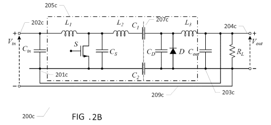
FIG. 2B) is an electrical circuit diagram of a class E resonant step-down DC-
DC
power converter 200c comprising a series resonant circuit in accordance with a
7th
embodiment of the invention. The class E resonant step-down DC-DC power con-
verter 200b may be obtained by conversion of the above-mentioned prior art
isolat-
ed class E resonant DC-DC converter 200 by inserting or adding an electrical
short
circuit connection 209c extending across a galvanic isolation barrier 207c of
the
converter 200c. The galvanic isolation barrier 207c comprises series
capacitors C1
and C2.The electrical short circuit connection 209c electrically connects the
negative
input terminal 201c and the first positive electrode 204c of the output
capacitor Cout.
The first positive electrode 204c is also connected to the converter output
voltage
Vont. As discussed in connection with FIG. 1C), the electrical short-circuit
connection
or wire 209c effectively places the output capacitor Cont and input capacitor
C,n in
series or cascade across the DC or AC input voltage V. Hence, the converter
load,
schematically illustrated by the load resistor RL, is coupled in parallel
across the out-
put capacitor Cont. The skilled person will understand that the series
capacitor C2 of
the galvanic isolation barrier 207c prevents DC current from flowing from the
second
negative electrode 203b of the output capacitor Cont and back to the negative
input
CA 02935004 2016-06-23
WO 2015/110427 PCT/EP2015/051007
terminal 201c. In this manner, the DC current is directed or forced through
the elec-
trical short circuit connection 209b and back through the input capacitor C.
In this
manner, despite being electrically by-passed by the conversion, the isolation
barrier
207c is important for the operation of the present class E resonant step-down
DC-
5 DC power converter 200c as otherwise would nodes 201c and 203c and 204c
be
directly electrically connected causing a short circuit at the converter
input.
The series resonant network of the converter core 205c of the converter 200c
may,
in addition to the above-discussed first and second series connected inductors
L1
10 and L2, comprise a capacitor (Cs) arranged across drain and source
terminals of the
MOSFET switch S to increase a resonant current and/or adjust/fine-tune a reso-
nance frequency of the power converter 200c. Likewise, a yet further capacitor
CD
may be arranged across the rectifying diode D to adjust a duty cycle of the
second-
ary part of the power converter 200c, i.e. the class E rectifier. During
operation of
15 the converter 200c, the series resonant network is excited by the MOSFET
switch S
such that the series resonant network is alternatingly charged from the DC or
AC
input voltage V,n and discharged to the output capacitor Cout through the
galvanic
isolation barrier 207c and through a rectification circuit comprising
inductance L3 and
diode D.
FIG. 3A) is an electrical circuit diagram of a prior art transformer isolated
class E
resonant DC-DC converter 300 comprising a series resonant circuit. A converter
core 305 of the converter 300 comprises a series resonant circuit which at
least in-
ductors L2, L3 and capacitors Cs and C1. The prior art DC-DC converter 300 com-
prises a primary side circuit and a secondary side circuit connected through a
gal-
vanic isolation barrier 307 provided by the transformer 308. The primary side
circuit
comprises a positive input terminal 302 and a negative input terminal 301 for
receipt
of a DC or AC input voltage V,n from a voltage or power source (not shown). An
in-
put capacitor C,n is electrically connected between the positive input
terminal 302
and a negative input terminal 301 to form an energy reservoir for the input
voltage
source. The primary side circuit additionally comprises a portion of a series
resonant
network or circuit which at least comprises inductors L2 and capacitors Cs and
C1. A
first inductor L1 has a first end coupled to the positive input terminal 302
and a sec-
ond end to a drain terminal of a MOSFET switch S which forms a switch arrange-
CA 02935004 2016-06-23
WO 2015/110427 PCT/EP2015/051007
26
ment of the present power converter 300. A secondary side circuit of the power
con-
verter 300 comprises an output capacitor Cnnt having a first electrode
electrically
connected to the converter output voltage Vont at output terminal 304. A
second
negative electrode of the output capacitor Cow is coupled to a negative
terminal 303
of the converter output voltage. An electrical or power converter load is
schematical-
ly illustrated by load resistor RI_ and coupled between the positive and
negative out-
put terminals 304, 303 of the prior art DC-DC converter 300. The secondary
side
circuit furthermore comprises the third inductor L3 connected across a
secondary
transformer winding of the above-mentioned transformer 308. The secondary
trans-
former winding has a first end coupled to a cathode of rectifying diode D and
a sec-
ond end coupled to the positive electrode of the output capacitor Cont. The
rectifying
diode D rectifies AC current generated by the secondary transformer winding
and
generates a DC voltage as the converter output voltage between the positive
and
negative output terminals 304, 303. An electrical or power converter load is
sche-
matically illustrated by load resistor RI_ coupled between the positive and
negative
output terminals 304, 303.
FIG. 3B) is an electrical circuit diagram of a transformer coupled class E
resonant
step-down DC-DC power converter 300c in accordance with an 8th embodiment of
the invention. The step-down DC-DC power converter 300c may be obtained by
conversion of the above-mentioned prior art resonant isolated DC-DC converter
300
by inserting or adding an electrical short circuit connection 309c extending
across a
galvanic isolation barrier formed by the transformer 308b. The transformer
308b
comprises magnetically coupled primary and secondary transformer windings with
the polarity inversion indicated by the black dots at the top of the windings.
A con-
verter core 305c of the converter 300 comprises a series resonant network or
circuit
which at least comprises inductors L2, L3 and capacitors Cs and C1. During
operation
of the converter 300c, the series resonant network is excited by the MOSFET
switch
S such that the series resonant network is alternatingly charged from the DC
or AC
input voltage V,n and discharged to the output capacitor Cnnt through the
galvanic
isolation barrier 307c and through a rectification circuit comprising diode D.
CA 02935004 2016-06-23
WO 2015/110427 PCT/EP2015/051007
27
The electrical short circuit connection 309c connects the negative input
terminal
302b of the primary side circuit and the first positive electrode 304c of the
output
capacitor Cow where the latter electrode also supplies the converter output
voltage.
As discussed in connection with FIGS. 1C), the electrical short-circuit
connection or
wire 309c effectively places the output capacitor Cout and input capacitor C,n
is series
or cascade across the positive and negative connections to the DC or AC input
volt-
age V. Hence, the converter load, schematically illustrated by the load
resistor IRL,
is coupled between the converter output voltage across the positive and
negative
electrodes of the output capacitor Cout. The skilled person will understand
that the
transformer coupling prevents DC current from flowing from the second negative
electrode 303c of the output capacitor Cout and back to the negative input
terminal
301c of the primary side circuit.
FIG. 4A) is an electrical circuit diagram of a prior art isolated single-ended
primary-
inductor converter (SEPIC) 400. The prior art SEPIC 400 comprises a primary
side
circuit and a secondary side circuit connected through a galvanic isolation
barrier
407. The primary side circuit comprises a positive input terminal 402 and a
negative
input terminal 401 for receipt of a DC or AC input voltage V,n from a voltage
or power
source (not shown). An input capacitor C,n is electrically connected between
the pos-
itive input terminal 402 and a negative input terminal 401 to form an energy
reservoir
for the input voltage source. A converter core 405 of the converter 400
comprises a
series resonant circuit which includes a first inductor L1 having first node
coupled to
the DC or AC input voltage V,n and a second node coupled to a drain terminal
of a
MOSFET switch S. A source terminal of a MOSFET switch S of a switch arrange-
ment is coupled to the negative input terminal 401. The prior art SEPIC 400 is
a res-
onant type of power converter wherein a resonance frequency of the converter
is
determined by the resonant network of the converter core 405 comprising the
first
and second inductors L1, L2 and the capacitors Cs and CD. The primary side
circuit is
arranged in front of a galvanic isolation barrier 407 within the converter
core 405 and
formed by coupling capacitors C1 and C2. The secondary side circuit comprises
an
output capacitor Cout having a first electrode electrically connected to the
converter
output voltage Vout at a positive output terminal 404. A second negative
electrode of
the output capacitor Cout is coupled to a negative terminal 403 of the
converter out-
put voltage. A rectifying diode D rectifies AC current generated by a second
inductor
CA 02935004 2016-06-23
WO 2015/110427 PCT/EP2015/051007
28
L2 and charges the output capacitor Cow such that the converter output voltage
Vout
between the positive and negative output terminals 404, 403 is a DC voltage. A
con-
verter load of the SEPIC 400, illustrated by load resistor RI_ is coupled
between the
positive and negative output terminals 404, 403.
FIG. 4B) is an electrical circuit diagram of a SEPIC 400c in accordance with a
9th
embodiment of the invention. The SEPIC 400c may be obtained by conversion of
the above-mentioned prior art SEPIC 400 by inserting or adding an electrical
short
circuit connection 409c extending across a galvanic isolation barrier 407c of
the
SEPIC 400c. The galvanic isolation barrier 407c comprises series capacitors C1
and
C2 which prevent the flow of DC current between the secondary side circuit and
the
primary side circuit in the isolated SEPIC 400 discussed above. In the present
SEPIC 400c, the electrical short circuit connection 409c electrically connects
the
negative input terminal 401c and the positive electrode 404c of the output
capacitor
Cout. As discussed in connection with FIGS. 1A) and 1B), the electrical short-
circuit
connection or wire 409c effectively places the output capacitor Cout and input
capaci-
tor C,n is series or cascade across the positive and negative connections to
the DC
or AC input voltage V,n such that the galvanic isolation between the primary
and
secondary side circuits is bypassed or eliminated. The electrical or power
converter
load, schematically illustrated by the load resistor IRL, is coupled between
the con-
verter output voltage Vout at the output terminal 404c and the negative
electrode
403c of the output capacitor. The skilled person will understand that the
series ca-
pacitor C2 of the galvanic isolation barrier 407b prevents DC current from
flowing
from the second negative electrode 403b of the output capacitor Cow and
directly
back to the negative input terminal 401b of the primary side circuit. The
SEPIC 400c
comprises a converter core 405c comprises a resonant network as discussed
above
comprising first and second inductors L1, L2 and capacitors Cs and CD. During
oper-
ation of the converter 400c, the series resonant network is excited by the
MOSFET
switch S such that the series resonant network is alternatingly charged from
the DC
or AC input voltage V,n and discharged to the output capacitor Cout through
the gal-
vanic isolation barrier 407c and through a rectification circuit comprising a
rectifying
diode D. The capacitor Cs connected or arranged across drain and source
terminals
of the MOSFET switch S is optional, but may be helpful to increase a resonant
cur-
rent and/or adjust/fine-tune a resonance frequency of the resonant network
SEPIC
CA 02935004 2016-06-23
WO 2015/110427
PCT/EP2015/051007
29
400c. In some embodiments of the SEPIC 400c the capacitor Cs may be formed
exclusively by a parasitic capacitance of the MOSFET S. The optional capacitor
CD
may be arranged across the rectifying diode D to adjust a duty cycle of the
power
converter 400c.