Note: Descriptions are shown in the official language in which they were submitted.
- 1-
ENCAPSULATED CONFORMAL ELECTRONIC SYSTEMS AND
DEVICES, AND METHODS OF MAKING AND USING THE SAME
CROSS-REFERENCE AND CLAIM OF PRIORITY TO RELATED PATENT APPLICATION
100011 This application claims the benefit of priority to U.S. Provisional
Patent
Application No. 61/924,111, which was filed on January 6, 2014, and U.S.
Provisional Patent
Application No. 61/947,709, which was filed on March 4, 2014.
TECHNICAL FIELD
[0002] Aspects of the present disclosure relate generally to flexible and
stretchable
integrated circuit (IC) electronics. More particularly, aspects of this
disclosure relate to
conformal electronic systems with encapsulated IC device islands.
BACKGROUND
[0003] Integrated circuits (IC) are the cornerstone of the information age
and the
foundation of today's information technology industries. The integrated
circuit, a.k.a.
"microchip," is a set of interconnected electronic components, such as
transistors, capacitors,
and resistors, which are etched or imprinted onto a tiny wafer of
semiconducting material, such
as silicon or germanium. Integrated circuits take on various forms including,
as some non-
limiting examples, microprocessors, amplifiers, Flash memories, application
specific integrated
circuits (ASICs), static random access memories (SRAMs), digital signal
processors (DSPs),
dynamic random access memories (DRAMs), erasable programmable read only
memories
(EPROMs), and programmable logic. Integrated circuits are used in innumerable
products,
including personal computers, laptop and tablet computers, smartphones, flat-
screen
televisions, medical instruments, telecommunication and networking equipment,
airplanes,
watercraft and automobiles.
[0004] Advances in integrated circuit technology and microchip
manufacturing have led
to a steady decrease in chip size and an increase in circuit density and
circuit performance.
The scale of semiconductor integration has advanced to the point where a
single
semiconductor chip can hold tens of millions to over a billion devices in a
space smaller than
a U.S. penny. Moreover, the width of each conducting line in a modern
microchip can be
Date Recue/Date Received 2022-04-13
- 2 -
made as small as a fraction of a nanometer. The operating speed and overall
performance of
a semiconductor chip (e.g., clock speed and signal net switching speeds) has
concomitantly
increased with the level of integration. To keep pace with increases in on-
chip circuit
switching frequency and circuit density, semiconductor packages currently
offer higher pin
counts, greater power dissipation, more protection, and higher speeds than
packages of just a
few years ago.
[0005] Conventional microchips are generally rigid structures that are not
designed to be
bent or stretched during normal operating conditions. Likewise, most
microchips and other IC
modules are typically mounted on a printed circuit board (PCB) that is
similarly rigid.
Processes using rigid IC's and rigid PCB's are generally incompatible for
applications
requiring stretchable or bendable electronics. Consequently, many schemes have
been
proposed for embedding microchips on or in a flexible polymeric substrate.
This, in turn,
enables many useful device configurations not otherwise possible with rigid
silicon-based
electronic devices. However, many of these schemes use embedded chips that are
thicker than
the individual layers of flexible polymer that make up the flexible printed
circuit board
assembly (FPCBA). Such schemes are not compatible for "thin chip"
configurations. In
addition, available processes for making flexible circuits oftentimes require
multiple layers of
expensive materials, which not only increases material and manufacturing costs
but also results
in a composite structure that is undesirably thick.
SUMMARY
[0006] Disclosed herein are encapsulated conformal electronic integrated
circuit (IC)
devices and conformal electronic systems with encapsulated IC device islands,
including
methods of making and methods of using the same. By way of example, there are
described
systems and methods for encapsulating conformal electronic devices, such as
conformal
electronic sensor assemblies. Said sensor assemblies may be used, for example,
for sensing,
measuring, or otherwise quantifying motion, including motion and/or muscle
activity of at
least one body part of a mammalian subject. In some examples, such conformal
electronic
sensor assemblies can be configured to attach directly to, lay against, and
monitor motion of a
human body part. Disclosed encapsulation methods can, for example, increase
the durability,
comfort, and/or aesthetic appeal of the conformal electronic devices described
herein, as well
as provide, for example, versatility, cost savings, and scale-up capability.
Date Recue/Date Received 2022-04-13
- 3 -
[0007] Also disclosed are processes for encapsulating at least a portion of
conformal
electronics into flexible and/or stretchable materials, such as soft
elastomeric materials.
Methods are disclosed for encapsulating relatively fragile conformal
electronics, such as a
flexible printed circuit board assembly (FPCBA), to generate more robust
devices that are
protected from mechanical and/or environmental damage. Inventive aspects of
this
disclosure are also directed to conformal electronic devices that include an
encapsulation
housing that envelops the entire conformal electronics device. Encapsulation
housings can be
stamped, molded or otherwise fabricated separately from the remainder of the
conformal
electronics device. The encapsulation housing can be molded or otherwise
generated as a
single-piece unitary structure that is disposed over portions of the conformal
electronic device
and laminated or otherwise attached thereto. Alternatively, encapsulation
housings can be
molded or otherwise generated in two or more separate housing components which
can be
coupled, assembled, or otherwise combined with an example conformal
electronics device to
provide an encapsulated conformal electronics device.
100081 Aspects of the present disclosure are directed to conformal
integrated circuit (IC)
devices. In an embodiment, a conformal IC device includes a flexible substrate
with
electronic circuitry attached to the flexible substrate. A flexible
encapsulation layer is
attached to the flexible substrate. The flexible encapsulation layer encases
the electronic
circuitry between the flexible substrate and the encapsulation layer. For some
configurations,
the encapsulation layer and flexible substrate are fabricated from stretchable
and bendable
non-conductive polymers. The polymer may include a polyimide (PI), a
polyethylene
terephthalate (PET), a silicone, or a polyurethane, or any combination
thereof. The electronic
circuitry may comprise an integrated circuit sensor system with at least one
sensing device
and at least one controller device. The electronic circuitry may comprise
multiple spaced
device islands that are electrically and physically connected via a plurality
of stretchable
electrical interconnects.
100091 In another embodiment, a conformal integrated circuit (IC) device
includes a flexible
substrate, electronic circuitry attached to the flexible substrate, and a
flexible polymeric
encapsulation layer attached to the flexible substrate, the flexible polymeric
encapsulation
layer forming a vaulted compartment encasing therein at least a portion of the
electronic
circuitry between the flexible substrate and the vaulted compartment of the
flexible polymeric
encapsulation layer. In this embodiment, the vaulted compartment is separated
from a second
vaulted compartment by a recessed portion, and the flexible polymeric
encapsulation layer
Date Recue/Date Received 2022-04-13
- 4 -
and the flexible substrate have a collective thickness in the range of about
1.0 mm to about
2.0 mm.
100101 According to other aspects of the present disclosure, conformal
electronics
devices are disclosed. In an embodiment, a conformal electronics device
includes an
elongated flexible polymeric substrate, and a plurality of surface-mount
technology (SMT)
components configured as device islands attached to the flexible polymeric
substrate. A
plurality of stretchable interconnects electrically connect the SMT
components. The
conformal electronics device also includes a flexible polymeric encapsulation
layer that is
attached to the flexible polymeric substrate. The flexible polymeric
encapsulation layer
encases the SMT components and the stretchable interconnects between the
flexible substrate
and the encapsulation layer.
100111 In another embodiment, a conformal electronics device includes an
elongated flexible
polymeric substrate, a plurality of surface-mount technology (SMT) components
configured
as device islands attached to the elongated flexible polymeric substrate, a
plurality of
stretchable interconnects electrically connecting the SMT components, and a
flexible
polymeric encapsulation layer attached to the elongated flexible polymeric
substrate, the
flexible polymeric encapsulation layer forming a vaulted compartment encasing
therein at
least a portion of the SMT components and the stretchable interconnects
between the
elongated flexible polymeric substrate and the vaulted compartment of the
flexible polymeric
encapsulation layer. In this embodiment, the vaulted compartment is separated
from a second
vaulted compartment by a recessed portion, and the flexible polymeric
encapsulation layer
and the elongated flexible polymeric substrate have a collective thickness in
the range of
about 1.0 mm to about 2.0 mm.
100121 Other aspects of the present disclosure are directed to methods for
making and
methods for using flexible integrated circuits. In one aspect, a method for
encapsulating a
conformal electronic device is disclosed. The method includes: receiving or
providing a first
silicone sheet; receiving or providing a second silicone sheet; placing the
first silicone sheet
into an assembly fixture; dispensing a first shot of adhesive onto the first
silicone sheet;
placing flexible printed circuit board assemblies (FPCBA) on top of the first
shot of adhesive
in the assembly fixture; dispensing a second shot of adhesive onto the
flexible printed circuit
board assemblies; placing the second silicone sheet on top of the second shot
of adhesive in
the assembly fixture to create a stack; and, transporting the assembly fixture
with the first and
Date Recue/Date Received 2022-04-13
- 5 -
second silicone sheets and the flexible printed circuit board assemblies
through a roll
laminator.
100131 The method may further comprise, singly or in any combination:
cleaning bonding
surfaces of the silicone sheets prior to the placing the second silicone sheet
on top of the
second shot of adhesive; inspecting the silicone sheets prior to the cleaning
the bonding
surfaces; cleaning both sides of the flexible printed circuit board assemblies
prior to placing
the FPCBA's on top of the first shot of adhesive; inspecting the FPCBA's prior
to the
cleaning the sides of the FPCBA's; placing a protective laminant sheet over
the assembly
fixture prior to the transporting the assembly fixture through the roll
laminator; removing the
assembly fixture from the roll laminator and allowing the shots of adhesive to
cure; and/or
die cutting a plurality of encapsulated conformal electronic devices from the
cured stack.
100141 The above summary is not intended to represent every embodiment or
every
aspect of the present disclosure. Rather, the foregoing summary merely
provides an
exemplification of some of the novel aspects and features set forth herein.
The above
features and advantages, and other features and advantages of the present
disclosure, will
be readily apparent from the following detailed description of representative
embodiments
and modes for carrying out the present invention when taken in connection with
the
accompanying drawings and the appended claims.
BRIEF DESCRIPTION OF THE DRAWINGS
100151 FIG. 1 is a side-view illustration of an example of a conformal
electronics device
with an encapsulation layer in accord with aspects of the present disclosure.
100161 FIG. 2 is a side-view illustration of an example of a conformal
electronics device
with multiple encapsulation layers in accord with aspects of the present
disclosure.
100171 FIGS. 3A and 3B are plan-view and perspective-view illustrations,
respectively,
of an encapsulated conformal electronics device in accord with aspects of the
present
disclosure.
100181 FIG. 4 is a cross-sectional side-view illustration of a portion of
the conformal
electronics device presented in FIGS. 3A and 3B taken along line 4-4 in FIG.
3A.
100191 FIG. 5 is a process flowchart illustrating an exemplary method for
encapsulating a
conformal electronic device using an overmolding process in accord with
aspects of the
present disclosure.
Date Recue/Date Received 2022-04-13
- 6 -
[0020] FIG. 6 is a process flowchart illustrating a representative method
for encapsulating
a conformal electronics device using a lamination process in accord with
aspects of the
present disclosure.
100211 FIGS. 7A-7F present representative plate-molding tools for
encapsulating
electronic sensor devices using an overmolding process in accord with aspects
of the present
disclosure.
100221 FIGS. 8A-8D are perspective-view illustrations of various
encapsulated conformal
electronics devices in accord with aspects of the present disclosure.
100231 FIGS. 9A and 9B are plan-view and bottom perspective-view
illustrations,
respectively, of an encapsulated conformal electronics device in accord with
aspects of the
present disclosure.
100241 FIGS. 10A and 10B are top and bottom perspective-view illustrations,
respectively of another encapsulated conformal electronics device in accord
with aspects of
the present disclosure.
100251 FIGS. 11A-11H are top and bottom perspective-view illustrations of
various other
encapsulated conformal electronics devices in accord with aspects of the
present disclosure.
10026] FIGS. 12A -12D illustrate encapsulated conformal electronics devices
with an
optional fabric feature in accord with aspects of the present disclosure.
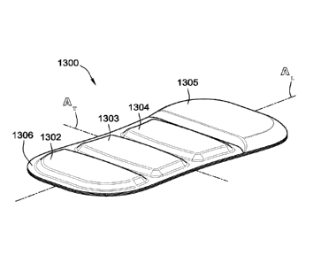
10027] FIGS. 13A -13C are perspective-view, plan-view and side-view
illustrations,
respectively, of an example of a conformal electronics device with a "waffle"
encapsulation
architecture in accord with aspects of the present disclosure.
100281 FIG. 14 is a diagrammatic illustration of yet another representative
method for
encapsulating a conformal electronic device in accord with aspects of the
present disclosure
100291 The present disclosure is susceptible to various modifications and
alternative
forms, and some representative embodiments have been shown by way of example
in the
drawings and will be described in detail herein. It should be understood,
however, that the
inventive aspects are not limited to the particular forms illustrated in the
drawings. Rather,
the disclosure is to cover all modifications, equivalents, and alternatives
falling within the
spirit and scope of the invention as defined by the appended claims.
DETAILED DESCRIPTION OF THE ILLUSTRATED EMBODIMENTS
100301 This disclosure is susceptible of embodiment in many different
forms. There are
shown in the drawings, and will herein be described in detail, representative
embodiments
Date Recue/Date Received 2022-04-13
- 7 -
with the understanding that the present disclosure is to be considered as an
exemplification of
the principles of the present disclosure and is not intended to limit the
broad aspects of the
disclosure to the embodiments illustrated. To that extent, elements and
limitations that are
disclosed, for example, in the Abstract, Summary, and Detailed Description
sections, but not
explicitly set forth in the claims, should not be incorporated into the
claims, singly or
collectively, by implication, inference or otherwise. For purposes of the
present detailed
description, unless specifically disclaimed or logically prohibited: the
singular includes the
plural and vice versa; and the words "including" or "comprising" or "having"
means
"including without limitation." Moreover, words of approximation, such as
"about,"
"almost," "substantially," "approximately," and the like, can be used herein
in the sense of
"at, near, or nearly at," or "within 3-5% of," or "within acceptable
manufacturing tolerances,"
or any logical combination thereof, for example.
100311 It should be understood that any and all combinations of the
features, functions
and concepts discussed in detail herein are contemplated as being part of the
inventive subject
matter (provided such concepts are not mutually inconsistent). For example,
although
differing in appearance, the individual systems and devices and functional
componentry
depicted and discussed herein can each take on any of the various forms,
optional
configurations, and functional alternatives described above and below with
respect to the
other disclosed embodiments, unless explicitly disclaimed or otherwise
logically prohibited.
It should be appreciated that various concepts introduced above and discussed
in greater
detail below may be implemented in any of numerous ways, as the disclosed
concepts are not
limited to any particular manner of implementation. Examples of specific
implementations
and applications are provided primarily for illustrative purposes.
100321 With respect to components, substrates, layers or other surfaces
described in the
Detailed Description in connection with various examples of the principles
herein, any spatial
references to "top" and "bottom" are used primarily to indicate relative
position, alignment,
and/or orientation of various elements/components with respect to the
component or substrate
and each other. These terms do not necessarily restrict to a particular frame
of reference
(e.g., a gravitational frame of reference) unless explicitly stated. Thus,
reference to a
"bottom" of a component, substrate, or a layer does not necessarily require
that the indicated
component, substrate, or layer be facing a ground surface. Similarly, other
terms of spatial
reference, such as "over," "under," "above," "beneath," and the like, do not
necessarily
restrict to a particular frame of reference, such as a gravitational frame of
reference, but rather
Date Recue/Date Received 2022-04-13
- 8 -
are used primarily to indicate relative position, alignment and/or orientation
of various
elements/components with respect to the substrate (or other surface) and each
other.
Moreover, use of the terms "disposed on" and "disposed over" in the Detailed
Description
encompass the meaning of "embedded in" and "partially embedded in," and vice
versa. In
addition, reference to feature A being "disposed on," "disposed between," or
"disposed over"
feature B in the Detailed Description encompasses examples where feature A is
in contact
with feature B, as well as examples where other layers and/or other components
are
positioned between feature A and feature B.
[0033] The terms "flexible" and "stretchable" and "bendable," including
roots and
derivatives thereof, when used as an adjective to modify electrical circuitry,
electrical
systems, and electrical devices or apparatuses, are meant to encompass
electronics that
comprise at least some components having pliant or elastic properties such
that the circuit is
capable of being flexed, stretched and/or bent, respectively, without tearing
or breaking or
compromising their electrical characteristics. These terms are also meant to
encompass
circuitry having components (whether or not the components themselves are
individually
stretchable, flexible or bendable) that are configured in such a way so as to
accommodate and
remain functional when applied to a stretchable, bendable, inflatable, or
otherwise pliant
surface. In configurations deemed "extremely stretchable," the circuitry is
capable of
stretching and/or compressing and/or bending while withstanding high
translational strains,
such as in the range of -100% to 100%, -1000% to 1000%, and, in some
embodiments, up to
¨100,000% to +100,000%, and/or high rotational strains, such as to an extent
of 1800 or
greater, without fracturing or breaking and while substantially maintaining
electrical
performance found in an unstrained state.
[0034] The encapsulated discrete "islands" or "packages" mentioned herein
are discrete
operative devices, e.g., arranged in a "device island" arrangement, and are
themselves
capable of performing the functionality described herein, or portions thereof.
Such
functionality of the operative devices can include, for example, integrated
circuits, physical
sensors (e.g. temperature, pH, light, radiation, etc.), biological sensors,
chemical sensors,
amplifiers, AID and D/A converters, optical collectors, electromechanical
transducers,
piezoelectric actuators, light emitting electronics (e.g., LEDs), and any
combination thereof.
A purpose and an advantage of using one or more standard ICs (e.g., CMOS on
single crystal
silicon) is to use high-quality, high-performance, and high-functioning
circuit components
that are readily accessible and mass-produced with well-known processes, and
which provide
Date Recue/Date Received 2022-04-13
- 9 -
a range of functionality and generation of data far superior to that produced
by passive
means. The discrete islands may range from about, but not limited to, 10-100
micrometers
( m) in size measured on an edge or by diameter.
100351 Examples described herein generally relate to systems and methods
for
encapsulating conformal electronics technology such as, for example, conformal
sensors for
sensing, measuring, or otherwise quantifying motion, including motion and/or
muscle activity
of at least one body part. In some examples, such conformal sensors can be
configured to
detect and/or quantify motion of a body part or other object. Such methods can
help to
increase the durability, comfort, and/or aesthetic appeal of the conformal
electronic devices
described herein, as well provide, for example, versatility, cost and scale-up
capability.
10036] According to at least some of the representative systems, methods,
and
apparatuses described herein, the example conformal sensors provide conformal
sensing
capabilities, providing mechanically transparent close contact with a surface
(such as the skin
or other portion of the body or the surface of an object) to improve
measurement and/or
analysis of physiological information of the body or other information
associated with the at
least one object. Conformal sensors of the example systems, methods, and
devices described
herein can be formed as patches. These patches are flexible and stretchable,
and can be
formed from conformal electronics and conformal electrodes disposed in or on a
flexible
and/or stretchable substrate. In various examples, the conformal electrodes
can be formed
integral with the conformal sensor, or can be made separable from the
conformal sensor.
100371 The example systems, methods and apparatuses described herein can be
used with
subjects that are humans or subjects that are non-human animals. The conformal
sensors can
be mounted to and caused to conform to, e.g., a portion of the skin or other
portion of the
body of the human or non-human animal, or the surface of an object.
100381 Disclosed conformal sensor systems and devices can be used for
sensing,
measuring and/or otherwise quantifying at least one parameter associated with
portions of the
body or other object. In another example, the systems, methods, and
apparatuses described
herein can be configured to use the results of analysis of data indicative of
at least one
parameter associated with portions of the body or other object, for such
applications as
medical diagnosis, medical treatment, physical activity, sports, physical
therapy and/or
clinical purposes. Data gathered using at least some of the disclosed
conformal sensors based
on sensing the at least one parameter associated with portions of the body or
other object,
along with data gathered based on sensing other physiological measures of the
body, can be
Date Recue/Date Received 2022-04-13
- 10 -
analyzed to provide useful information related to medical diagnosis, medical
treatment,
physical state, physical activity, sports, physical therapy, and/or clinical
purposes. When
sensing is performed using thin, conformal, and wearable sensors described
herein, or
measurement devices with such sensors, these measures and metrics can be
unimpeded by the
size, weight or placement of the measurement devices.
[0039] Example systems, methods, and apparatuses described herein provide
for creating,
building, and deploying thin and conformal electronics that are useful in a
wide variety of
applications, both inside the body and outside the body. The example conformal
sensors
include silicon-based and other electronics in new form factors allowing the
creation of very
thin and conformal devices.
[0040] Example systems, methods, and apparatuses described herein including
the
conformal sensors can be configured to monitor the body motion and/or muscle
activity, and
to gather measured data values indicative of the monitoring. The monitoring
can be
performed in real-time, continuously, systematically, at different time
intervals, and/or upon
request. In addition, at least some of the systems, methods, and apparatuses
described herein
can be configured to store measured data values to a memory of the system
and/or
communicate (transmit) the measured data values to an external memory or other
storage
device, a network, and/or an off-board computing device. In any example
herein, the external
storage device can be a server, including a server in a data center. Non-
limiting examples of
computing devices applicable to any of the embodiments according to the
principles herein
include smartphones, tablets, laptops, slates, e-readers or other electronic
reader or hand-held
or worn computing device, an Xbox0, a Wii0, or other game system(s).
[0041] This example systems, methods, and apparatus can be used to provide
ultra-thin
and conformal electrodes that facilitate monitoring and diagnosis of subjects,
including when
combined with measurements of at least one parameter associated with portions
of the body
or other object. In combination with pharmaceuticals, this information can be
used to
monitor and/or determine subject issues including compliance with and/or
effects of,
treatment regimens.
[0042] The example conformal sensors can be configured to provide a variety
of sensing
modalities. Example conformal sensors can be configured with sub-systems such
as
telemetry, power, power management, processing as well as construction and
materials. A
wide variety of multi-modal sensing systems that share similar design and
deployment can be
fabricated based on the example conformal electronics.
Date Recue/Date Received 2022-04-13
- 11 -
[0043] According to aspects of the disclosed concepts, conformal sensors
can be
configured to include electronics for performing measurements of at least a
parameter of an
object or a body part that is proximate to the conformal sensor. An example
conformal
sensor system can include electronics for performing at least one of an
accelerometry
measurements and a muscle activation measurement. In other examples, the
conformal
sensor system can include electronics for performing at least one other
measurement, such as
but not limited to heart rate measurements, electrical activity measurements,
temperature
measurements, hydration level measurements, neural activity measurements,
conductance
measurements, environmental measurements, and/or pressure measurements. For
example,
the conformal sensors can be configured to perform any combination of two or
more of these
different types of measurements.
[0044] Referring now to the drawings, wherein like reference numerals refer
to like
components throughout the several views, FIG. 1 illustrates a conformal
electronics device,
designated generally at 100, which includes a substrate 110, electronic
circuitry 120, and an
encapsulation layer 130. Conformal electronics device 100, for some
implementations, is
configured to provide conformal sensing and/or monitoring capabilities. The
device 100 can
provide mechanically transparent close contact with a surface (e.g., the skin
or other portion
of the body or the surface of an object) to improve measurement and/or
analysis of
physiological information of the body or other information associated with the
at least one
object.
[0045] The substrate 110 can, for example, be a soft, flexible, or
otherwise stretchable
substrate of non-conductive material that can conform to the contour of a
surface on which
the conformal electronics device 100 is disposed. Examples of such surfaces
include, but are
not limited to, a body part of a human or an animal or any other object.
Suitable substrates
110 that can be used in the conformal electronics device 100 include, for
example, a polymer
or a polymeric material. Non-limiting examples of applicable polymers or
polymeric
materials include, but are not limited to, a polyimide (PI), a polyethylene
terephthalate (PET),
a silicone, or a polyurethane. Other non-limiting examples of applicable
polymers or
polymeric materials include plastics (including a thermoplastic, a thermoset
plastic, or a
biodegradable plastic), elastomers (including a thermoplastic elastomer, a
thermoset
elastomer, or a biodegradable elastomer), and fabrics (including a natural
fabric or a synthetic
fabric), such as but not limited to acrylates, acetal polymers, cellulosic
polymers,
fluoropolymers, nylons, polyacrylonitrile polymers, polyamide-imide polymers,
polyarylates,
Date Recue/Date Received 2022-04-13
- 12 -
polybenzimidazole, polybutylene, polycarbonate, polyesters, polyetherimide,
polyethylene,
polyethylene copolymers and modified polyethylenes, polyketones, poly(methyl
methacrylate, polymethylpentene, polyphenylene oxides and polyphenylene
sulfides,
polyphthalamide, polypropylene, polyurethanes, styrenic resins, sulphone based
resins, vinyl-
based resins, or any combinations of these materials. In an example, a polymer
or polymeric
material herein can be a UV curable polymer, such as but not limited to a UV
curable
silicone.
100461 The substrate 110 can be formed using any suitable process
including, for
example, casting, molding, stamping, or any other suitable process.
Furthermore, the
substrate 110 can include other features, for example, holes, protrusions,
grooves, indents,
non-conducting interconnects, or any other features. In some examples,
grooves, which can
act as seats for device islands or interconnects, can be formed on the
substrate 110.
100471 Electronic circuitry 120 can be any suitable electronic circuitry
that is operable,
for example, to provide sensing, detecting, or otherwise quantifying at least
one parameter
associated with a subject or a surface (e.g., an animal or human body part or
other object) on
which the conformal electronics device 100 is disposed. For instance, the
electronic circuitry
120 is configured to measure, detect, sense, or otherwise quantify motion,
muscle activity,
temperature (e.g., body temperature), pulse, moisture, pressure, and the like.
The electronic
circuitry 120 can include one or more sensor system(s), and one or more other
component(s)
(e.g., interconnects). The one or more sensor systems and one or more other
component(s)
are disposed on one or more device islands. The one or more device islands are
arranged in a
spatial configuration based on the desired dimensions and conformability of
the overall
resulting conformal electronic devices.
100481 The one or more sensor systems included in the electronic circuitry
120 can
include at least one component to perform at least one sensor measurement. Non-
limiting
examples of the at least one sensor measurement include an accelerometry
measurement, a
muscle activation measurement, a heart rate measurement, an electrical
activity measurement,
a temperature measurement, a hydration level measurement, a neural activity
measurement, a
conductance measurement, an environmental measurement, and/or a pressure
measurement.
As non-limiting examples, the sensor systems can include, one or more of an
accelerometer
(such as but not limited to a single-axis accelerometer or a 3-axis
accelerometer), a gyroscope
(such as but not limited to a 3-axis gyroscope), a nerve conduction study
(NCS) component,
Date Recue/Date Received 2022-04-13
- 13 -
an electromyography (EMG) component, an electroencephalogram (EEG) component,
and/or
an electrocardiogram (ECG) component.
[0049] Non-limiting examples of other components that can be included in
the electronic
circuitry 120 include at least one battery, a regulator, a processing unit, a
memory (such as
but not limited to a read-only memory, a flash memory, and/or a random-access
memory), an
input interface, an output interface, a communication module, a passive
circuit component, an
active circuit component, etc. In an example, the conformal electronics device
100 comprises
at least one microcontroller and/or other integrated circuit component. In an
example, the
electronic circuitry 120 includes at least one coil, such as but not limited
to a near-field
communication (NFC) enabled coil. In another example, the electronic circuitry
120 includes
a radio-frequency identification (RFID) component. In the same regard, the
electronic
circuitry 120 can include a dynamic NFC/RFID tag integrated circuit with a
dual-interface,
electrically erasable programmable memory (EEPROM).
[0050] The configuration of the device islands can be determined based on,
e.g., the type
of components that are incorporated in the overall electronic circuitry 120
(including the
sensor system), the intended dimensions of the overall conformal electronics
device 100, and
the intended degree of conformability of the overall conformal electronics
device 100. As a
non-limiting example, the configuration of one or more device islands can be
determined
based on the type of overall conformal electronics device 100 to be
constructed. For
instance, the overall conformal electronics device 100 may be a wearable
conformal
electronics structure, or a passive or active electronic structure that is to
be disposed in a
flexible and/or stretchable object (including an inflatable or expandable
surface of an
interventional catheter). Optionally, the configuration of the device
island(s) can be
determined based on the components to be used in an intended application of
the overall
conformal electronics device 100. Example applications include a motion
sensor, a
temperature sensor, a neuro-sensor, a hydration sensor, a heart sensor, a flow
sensor, a
pressure sensor, an equipment monitor (e.g., smart equipment), a respiratory
rhythm monitor,
a skin conductance monitor, an electrical contact, or any combination thereof.
One or more
device islands can be configured to include at least one multifunctional
sensor, including a
temperature, strain, and/or electrophysiological sensor, a combined motion-
/heart/neuro-
sensor, a combined heart-/temperature-sensor, etc. Examples of electronic
circuitry and
conformal electronics devices including electronic circuitry are described in
U.S. Provisional
Date Recue/Date Received 2022-04-13
- 14 -
Patent Application No. 61/907,973, filed November 22, 2013, and entitled
"Configuration of
Conformal Sensor Systems for Sensing and Analysis".
100511 The
encapsulation layer 130 is disposed on at least a portion of the electronic
circuitry 120 and at least a portion of the substrate 110 such that the
encapsulation layer 130
envelops at least a portion of the electronic circuitry 120. In some
configurations, such as
that shown, encapsulation layer 130 is formed of a material that hermetically
seals portions
(e.g., surfaces) of the electronic circuitry 120 exposed by the substrate 110.
Optionally, the
encapsulation layer 130 can act as an "encapsulation housing" by enveloping
most or all of
the conformal electronics device 100. For some implementations, the
encapsulation layer
130 is disposed on the device islands and interconnects of the electronic
circuitry 120
hermetically sealing the device islands and interconnects. In such
instances, the
encapsulation layer 130 can include holes, apertures, or otherwise openings
such that one or
more sensors included in the electronic circuitry 120 are exposed (e.g., to
contact a skin or
body part of an animal or human, or any other object). Hermetically sealing at
least a portion
of the electronic circuitry 120 by the encapsulation layer 130 can help to
protect the
components of the electronic circuitry 120 from corrosive factors, including
damage from
corrosive chemicals, dust, moisture, oxidation, etc.
100521
Encapsulation layer 130 of FIG. 1 can be formed from a soft, flexible, and non-
conductive material. In some examples, the encapsulation layer 130 is formed
from the same
material as the substrate 110. In other examples, a different material can be
used to form the
encapsulation layer 130. Suitable materials that can be used in the
encapsulation layer 130
include, for example, a polymer or a polymeric material. Non-limiting examples
of
applicable polymers or polymeric materials include, but are not limited to, a
polyimide (PI), a
polyethylene terephthalate (PET), a silicone, or a polyurethane. Other non-
limiting examples
of applicable polymers or polymeric materials include plastics (including a
thermoplastic, a
thermoset plastic, or a biodegradable plastic), elastomers (including a
thermoplastic
elastomer, a thermoset elastomer, or a biodegradable elastomer), and fabrics
(including a
natural fabric or a synthetic fabric), such as but not limited to acrylates,
acetal polymers,
cellulosic polymers, fluoropolymers, nylons, polyacrylonitrile polymers,
polyamide-imide
polymers, polyarylates, polybenzimidazole, polybutylene, polycarbonate,
polyesters,
polyetherimide, polyethylene, polyethylene copolymers and modified
polyethylenes,
polyketones, poly(methyl methacrylate, polymethylpentene, polyphenylene oxides
and
polyphenylene sulfides, polyphthalamide, polypropylene, polyurethanes,
styrenic resins,
Date Recue/Date Received 2022-04-13
- 15 -
sulphone based resins, vinyl-based resins, or any combinations of these
materials. In an
example, the polymer or polymeric material can be a UV curable polymer, such
as a
ultraviolet (UV) curable silicone.
100531 With continuing reference to FIG. 1, the encapsulation layer 130 can
be formed
using any suitable process, for example, casting, molding, stamping, or any
other known or
hereinafter developed fabrication methods. Furthermore, the encapsulation
layer 130 can
include a variety of optional features, such as holes, protrusions, grooves,
indents, non-
conducting interconnects, or any other features. By way of non-limiting
example,
encapsulation layer 130 can be formed using an overmolding process. In
general,
overmolding allows for a previously fabricated part to be inserted into a
mould cavity an
injection molding machine that forms a new plastic part, section, or layer on
or around the
first part. One such overmolding process includes directly casting a liquid
material capable
of forming the encapsulation layer 130 on the electronic circuitry 120
disposed on the
substrate 110. The liquid material can then be cured (e.g., cool and
solidify). Curing can be
performed under any suitable conditions, for example, by applying pressure on
the casted
liquid material, heating the substrate, and/or applying a vacuum.
100541 As another example, the electronic circuitry 120 can be embedded in
the
encapsulation layer 130 using a lamination process. For instance, the
encapsulation layer 130
can be precasted into a sheet. A liquid adhesive (e.g., the uncured liquid
material used to
form the encapsulation layer, or any other suitable adhesive) can then be
disposed on the
electronic circuitry 120 and the substrate 110. The encapsulation layer 130
can be then
disposed on the adhesive and pressure applied to squeeze out excess adhesive.
The adhesive
can then be cured to fixedly couple the encapsulation layer 130 to at least a
portion of the
electronic circuitry 120 and the substrate 130, thereby forming conformal
electronics device
100 of FIG. 1.
100551 According to aspects of the disclosed concepts, an adhesive material
can be used
during construction of encapsulated conformal electronic devices. Further to
the options
discussed above, the uncured liquid silicones used in the example lamination
process can act
as a type of adhesive, and harden, e.g., via curing (through crosslinking) to
bind surfaces. In
other examples, the electronic device components, including the device islands
and electrical
interconnects, can be affixed to a pre-cured sheet using a pressure sensitive
adhesive prior to
overmolding. A non-limiting example of a pressure sensitive adhesive is a
rubber-based
adhesive. In an example, in the construction of a patch including a sensor
component (such
Date Recue/Date Received 2022-04-13
- 16 -
as a temperature sensor or an electromagnetic radiation sensor (such as a UV
sensor)), a
pressure sensitive silicone transfer adhesive or a liquid silicone adhesive
can be applied to the
pre-cured sheet. Any adhesive described herein may be a sprayable or a
brushable adhesive
for application to a surface. An adhesive can aid in holding the electronic
components in a
specified position and arrangement, including in an archipelago arrangement,
relative to other
components of the system, during a subsequent overmolding process.
100561 Adhesive materials can be used as a part of the lamination process
during
construction of an example device herein. For example, the electronic device
components,
including the device islands and/or the interconnects, can be affixed to a pre-
cured base layer
silicone sheet using a pressure sensitive silicone adhesive prior to applying
the top layer of
silicone sheet, with an uncured liquid silicone used for lamination. In other
examples, the
lamination can also be completed using a pressure sensitive silicone adhesive
to embed an
ultrathin electronics device between silicone sheets. The lamination can be
based on use of a
film adhesive that does not require a curing process.
100571 Encapsulation layer 130 and/or base substrate 110 of FIG. 1 can be
configured to
facilitate modulation of a stress or a strain that might be caused in a
portion of the conformal
electronics device 100, for example, due to stretching, bending, compressing,
torsion, or other
deformation. As an example, there can be a concentration of stress and/or
strain at a
transition from a more rigid portion of a system (e.g., a device island) to a
more compliant
structure (e.g., a flexible and/or stretchable component) when the conformal
electronics
device 100 is subjected to a deformation. Other areas of stress concentration
can include, for
example, edges of interconnects, or boundaries where an interconnect is
coupled to a device
island. Encapsulation layer 130 can be formed from a material that is
configured to have a
thickness and/or disposed locally on portions of the electronic circuitry 120
such as to
minimize the stress on the components of the electronic circuitry 120 by
adjusting the
location of a neutral mechanical plane relative to a functional component of
the electronic
circuitry. For example, the material used to form the encapsulation layer 130
can be
introduced locally in a region of a component of the electronic circuitry 120,
such as
proximate to the portion of the component of the electronic circuitry 120. The
locally
disposed encapsulation layer protects the component from applied
stresses/strains in the event
of a deformation force being applied to the overall conformal electronics
device 100 by
adjusting the location of the neutral mechanical plane locally in the region
of the component.
Controlled placement of the neutral mechanical plane relative to a functional
component can
Date Recue/Date Received 2022-04-13
- 17 -
result in little to no stress or strain being exerted in the region of the
component, when the
conformal electronics device 100 is subjected to a deformation force.
100581 In the embodiment illustrated in FIG. 1, the encapsulation layer 130
and/or
substrate 110 can have an ultrathin thickness and have favorable mechanical
and optical
properties. Optionally, the encapsulation layer 130 can have a thickness in
the range of about
0.05 mm to about 0.5 mm. Moreover, the encapsulation layer 130 and/or the
substrate 110
can have an elongation in the range of about 200% to about 800% or, for some
configurations, about 300%, about 400%, about 500%, about 600%, or about 700%,
relative
to the undeformed length of the encapsulation layer 130/substrate 110. In some
examples,
the encapsulation layer 130 and/or the substrate 110 have a tear strength of
about 40 pounds
per inch (ppi) to about 200 ppi or, for some configurations, about 60 ppi,
about 80 ppi, about
100 ppi, about 120 ppi, about 140 ppi, about 160 ppi, or about 180 ppi. As
another option,
the encapsulation layer 130 and/or the substrate 110 can have a hardness
measured by a
durometer of about 10 A (e.g., according to the Shore A Hardness Scale) to
about 60A to
higher, for example, about 20 A, about 30 A, about 40 A, about 50 A or about
60 A. For
some configurations, the encapsulation layer 130 and/or the substrate 110 can
have an optical
transparency of greater than about 90% between wavelengths of light about 350
nm to about
1,000 nm. The total thickness of encapsulated conformal electronics device 100
(e.g., at its
thickest point) can be in the range of about 0.20 mm to about 1.0 mm. For some
configurations, the encapsulation layer 130 and/or the substrate 110 can be
transparent. In
other examples, the encapsulation layer 130 and/or the substrate 110 can be
translucent or
colored. In some examples, a conformal electronic device can be encapsulated
using a
plurality of thin encapsulation layers.
100591 Referring next to FIG. 2, a representative encapsulated conformal
electronics
device is shown in accordance with aspects of the present disclosure. Similar
to the device
architecture presented in FIG. 1, conformal electronics device 200 of FIG. 2
includes, as
some non-limiting examples, electronic circuitry 220 that is coupled to a
substrate 210. The
substrate 210 and the electronic circuitry 220 can be substantially similar to
the substrate 110
and the electronic circuitry 120, respectively, described with respect to the
conformal
electronics device 100. For example, the substrate 210 and the electronic
circuitry 220 can
each take on any of the various forms, optional configurations, and functional
alternatives
described above with respect to the corresponding structure illustrated in
FIG. 1.
Date Recue/Date Received 2022-04-13
- 18 -
[0060] A series of encapsulation layers ¨ first, second, third and fourth
encapsulation
layers 230a, 230b, 230c and 240d, respectively (collectively referred to as
"encapsulation
layers") in FIG. 2 - are disposed sequentially on the substrate 210 and
circuitry 220, with the
top three layers 230b-d operating to strengthen the first encapsulation layer
230a. Each
encapsulation layer 230a-d can be an ultrathin layer, for example, having a
thickness in the
range of about 0.05 mm to about 0.5 mm. The encapsulation layers 230a-d of
FIG. 2 can be
formed from any of the materials described above with respect to conformal
electronics
device 100 of FIG. 1. While shown as having four encapsulation layers 230a-d,
any number
of encapsulation layers can be used to encapsulate the device 200. Moreover,
while FIG. 2
shows each of the encapsulation layers covering the entire width of the device
200, in some
examples, one or more of the various encapsulation layers 230a-d can be
disposed on only a
portion of the electronic circuitry 220 and/or the substrate 210. For example,
one or more of
the plurality of encapsulation layers 230a-d can be disposed in proximity to
an area of
stress/strain concentration (e.g., a device island or edges of interconnects),
thereby adjusting
the location of a neutral mechanical plane relative to a functional component
of the electronic
circuitry.
100611 FIGS. 3A and 3B show the mechanical layout and system-level
architecture of an
example conformal electronics device, designated 300, configured as a
rechargeable patch.
The example conformal sensor system electronics technology can be designed and
implemented with various mechanical and electrical layouts for single-function
and
multifunctional platforms. Devices including the conformal electronics
technology
integrate stretchable form factors using designs embedded in polymeric layers.
These can
be formulated to protect the circuits from strain and to achieve mechanical
flexibility in an
ultra-thin cross-section. For example, the device can be configured with
thicknesses on the
order of about 1 mm on average. In other examples, the patch can be configured
with
thinner or thicker cross-sectional dimensions. The device architecture can
include a
reusable module containing surface-mount technology (SMT) components,
including as
some non-limiting examples, a sensor module 302 (e.g., a triaxial
accelerometer), a wireless
communication (e.g., Bluetooth0) and microcontroller (MCU) module 304, and
conformal
electrode array modules 312 and 314 for sensing, e.g., EMG, EEG and EKG
signals, with
electrode connectors 313. The conformal electrode arrays can be disposable 310
and 312.
The example device can also include a power supply 316 (such as a LiPo Battery
of power
Date Recue/Date Received 2022-04-13
- 19 -2mA-Hr or 10 mA-Hr), a regulator 318, a power transfer coil 320 (such as
but not limited
to a 0.125 oz Cu coil with 1.5/2 mil trace/space ratio), and a memory 322.
100621 As shown in the example of FIGS. 3A and 3B, the components of the
example
conformal sensor system 300 are configured as device islands interconnected by
stretchable
interconnects 328. Stretchable interconnects 328 can be electrically
conductive to facilitate
electrical communication between the components, or electrically non-
conductive to assist
in maintaining a desired overall form factor or relative aspect ratio of the
overall
conformation of the conformal sensor device during or after being subjected to
deformation
forces, such as but not limited to extension, compressive and/or torsional
forces. The
example of FIG. 3 also shows the differing shapes and aspect ratios of the
island bases 326
that the components of the example conformal sensor system can be disposed on,
or
otherwise coupled to, to provide the to provide the necessary functionality of
the overall
system.
100631 Conformal electronics device 300 of FIGS. 3A and 3B comprises a
flexible
substrate 310, such as flexible substrates 110 and 210 of FIGS. 1 and 2,
respectively, to
which is coupled the electronic circuitry. Substrate 310 and electronic
circuitry are at least
partially encapsulated by a flexible encapsulating layer 330. Electronic
circuitry included in
the conformal electronics device 300 includes a plurality of device islands
(ten of which are
shown in the drawing, two of which are designated at 326) that are
electronically coupled
together via serpentine interconnects 328. In some example implementations,
such as
illustrated in FIGS. 3A-3B, a plurality of contacts may be disposed at either
or each end of
the conformal electronics device 300. In other example implementations, the
conformal
electronic device does not include such contacts. The device islands can
include any number
of interconnects and any number of components as described with respect to
conformal
electronics device 100 or any other conformal electronic devices described
herein.
100641 FIG. 4 shows a cross-section of a portion of the conformal
electronics device 300
taken along line 4-4 in FIG. 3A. As seen in FIG. 4, the device 300 includes a
substrate 310
providing subjacent support for a base plate 340 disposed on the substrate
310. Substrate 310
can be formed from, for example, RTV silicone or any other suitable substrate
material
described herein. In some examples, the substrate 310 can have a thickness of
about 200 p.m.
In some examples, the base plate can be formed from polyimide and, optionally,
can have a
thickness of about 50 [im. One or more electrical contacts 342 are disposed on
the base plate
310 and coupled to the electronic component 344. The electronic component 344
can be any
Date Recue/Date Received 2022-04-13
- 20 -
component described with respect to the conformal electronics device 100, or
any other
electronic components described herein. For some configurations, the
electronic component
344 has a thickness of about 500 um. The electrical contact(s) 342 can be
formed from any
suitable electrically conductive material, such as copper. Electrical
contact(s) 342 can have a
thickness of about 0.5 um. Select (upper and side) portions of the electrical
contact 342 not
coupled with the electronic component 344 are covered with an insulating layer
346.
100651 An encapsulation layer 330 is disposed on the substrate 310 such
that the
encapsulation layer completely encapsulates the entire conformal electronic
device 300 (or
substantially all of the device). In some examples, the encapsulation layer
330 can be formed
from RTV silicone or any other encapsulation material described herein. While
the
conformal electronic device 300 is shown and described as having certain
components, the
conformal electronics device 300 can include any of the other components
described herein
which can be configured to perform any suitable function as described herein.
For some
example architectures, the encapsulating layer 330 is configured to define an
ultrathin
thickness such that the thickness of the encapsulation layer 330, as measured
from a distal
end of the electronic component, is approximately 200 um. In such examples,
the conformal
electronic devices have an ultrathin profile, e.g., having a maximum thickness
at its thickest
point of less than about 2 mm or, in some embodiments, less than about 1 mm.
100661 As shown in FIG. 4, the encapsulating layer 330 can be disposed
locally over, or
proximate to, a portion of the base plate 340, electronic component 344,
and/or an
interconnect 328. For example, the encapsulating layer can be disposed over,
or proximate
to, portions of the overall conformal electronic device 300 device structure,
including one or
more electronic components, base plates, and/or interconnects. An
encapsulation material
can be introduced locally in a region of a portion of a component of the
conformal electronic
device 300, such as proximate to the portion of the component, to protect the
component
from an applied stress or strain in the event of a deformation force being
applied to the
overall conformal device. For example, the encapsulation material can aid in
adjusting a
location of a neutral mechanical plane locally in the region of the component.
Controlled
placement of the neutral mechanical plane relative to a functional component
can result in
cause little to no stress or strain being exerted in the region of the
component, when the
overall conformal electronic device 300 is subjected to the deformation force.
100671 With continuing reference to FIG. 4, base plate stiffness can result
in the
interconnect coupled to the base plate being subjected to a greater amount of
plastic strain on
Date Recue/Date Received 2022-04-13
- 21 -
deformation, e.g., a stretching. As a non-limiting example, a base plate
formed from a
polyimide (PI) or a polyethylene terephthalate (PET) can have a value of
modulus of about
6.894MPa and a C10 (a hyper-elasticity material constant) of about is
0.925MPa. In
determining the configuration of the overall conformal device, the dimensions
of, and/or
stiffness of the material of, the base plate can be considered, in conjunction
with the stiffness
properties and/or placement of the encapsulant material, can be controlled to
strategically to
urge the neutral mechanical plane to fall in a region of the overall conformal
device to
prevent such a strain concentration near the passive component and/or the
interconnects.
100681 Also disclosed herein are methods for making and methods for using
encapsulated
conformal electronic devices. Some of these methods will be described with
reference to the
various configurations and features shown in FIGS. 1 through 4 of the
drawings; such
reference is being provided purely by way of explanation and clarification. In
some
embodiments, such as those shown in FIGS. 5, 6 and 14, each method includes at
least those
steps enumerated in its respective figure. It is also within the scope and
spirit of the present
disclosure to omit steps from each method, include additional steps in each
method, and/or
modify the order presented. It should be further noted that each of the
foregoing methods can
be representative of a single sequence of related steps; however, it is
expected that each of
these method will be practiced in a systematic and repetitive manner.
100691 FIG. 5 presents a flow diagram showing an exemplary method 400 for
encapsulating a conformal electronic device, such as the conformal electronics
device 100
and 200 of FIGS. 1 and 2, or any other conformal electronic device described
herein, using
overmolding. The method 400 begins at Block 402 with disposing a substrate
material into a
first mold. The substrate material can include, for example, any of the
materials used to form
the substrate 110, substrate 210, or any other substrate described herein.
Before disposing the
substrate material into the first mold, the first mold can be cleaned using
any suitable process.
In some examples, a release layer, such as wax, oil, soapy water, or any other
suitable release
layer, is disposed on the first mold before adding the substrate material. The
release layer can
allow for easy removal of the substrate from the first mold after curing.
100701 At Block 404, the substrate material is cured to form a soft and
flexible substrate.
Any suitable curing process can be used. For example, a positive pressure can
be applied on
the first mold, the first mold can be heated to a predetermined temperature,
and/or a vacuum
can be applied on the first mold. Electronic circuitry is next disposed on the
cured substrate
at Block 406. The electronic circuitry can include, for example, the
electronic circuitry 120,
Date Recue/Date Received 2022-04-13
- 22 -
electronic circuitry 220, or any other electronic circuitry described herein,
including those
identified in FIG. 3A. An encapsulation material is disposed in a second mold
at Block 408
of the method 400 in FIG. 5. The encapsulation material can include, for
example, the
materials used for forming the encapsulation layer 130, encapsulation layer
230, or any other
encapsulation materials described herein. In some examples, a release layer,
such as wax, oil,
soapy water, or any other suitable release layer, is disposed on the second
mold before adding
the encapsulation material. The release layer allows for easy removal of the
encapsulation
material from the second mold after curing.
100711 Continuing with the exemplar method of FIG. 5, Block 410 includes
positioning
the first mold, which includes the substrate and the electronic circuitry
disposed on the
substrate, in an inverted position (e.g., upside down) on the second mold. The
first mold and
the second mold are then cured to form the encapsulated conformal electronic
device at Block
412. Any suitable curing process can be used. For instance, a positive
pressure can be
applied on the first mold and the second mold, the first mold and the second
mold can be
heated to a predetermined temperature, and/or a vacuum can be applied on the
first mold and
the second mold. After curing, the encapsulated conformal electronic device
can be removed
from the first mold and the second mold at Block 414,
100721 FIG. 6 is a flow diagram showing an exemplary method 500 for
encapsulating
conformal electronic devices, such as the conformal electronics device 100,
200, or any other
conformal electronic device described herein, using lamination. The method 500
of FIG. 6
begins at Block 502 with cutting a fully cured sheet of a stretchable material
to a
predetermined size to form a substrate. The stretchable material can include
any of the
materials described with respect to the substrate 110, substrate 210, or any
other stretchable
materials described herein. An uncured lamination material is then disposed on
the
stretchable material at Block 504. The lamination material can include any
suitable material,
for example, the stretchable material used to form the substrate described
herein. In some
examples, the lamination material can include the material used to form an
encapsulation
layer.
100731 Next, at Block 506, electronic circuitry is disposed on the uncured
lamination
material. The electronic circuitry can include the electronic circuitry 120,
electronic circuitry
220, or any other electronic circuitry described herein. Excess amounts of the
uncured
lamination material is then disposed on the electronic circuitry, e.g., at
Block 508, such that
the electronic circuitry is completely covered with the lamination material. A
sheet of a fully
Date Recue/Date Received 2022-04-13
-23 -
cured encapsulating material (i.e., the encapsulation layer) is disposed on
the uncured
lamination material at Block 510. The encapsulation layer can be formed from
any of the
encapsulation materials described with reference to the encapsulation layer
130, or any other
encapsulation materials described herein. Pressure can be applied on the
encapsulation layer
to remove excess lamination material. The encapsulation material is then cured
to form the
encapsulated conformal electronic device at Block 512. Any suitable curing
process can be
used. For example, a positive pressure, heat or a vacuum can be used to cure
the lamination
material. Curing the lamination layer couples together the substrate sheet,
the electronic
circuitry, and the encapsulation sheet to form the encapsulated conformal
electronic device.
100741 The following are some representative implementations that show
examples of
various encapsulated conformal electronic devices formed using processes and
methods
according to the principles described herein. These examples are only for
illustrative
purposes and are not intended to limit the scope of the present disclosure.
EXAMPLE 1
100751 In this example, a conformal electronic device - hereinafter "Ex 1
Device" - which
includes moisture sensors is encapsulated using an overmolding process. The Ex
1 Device is
encapsulated to have a final thickness of about 6 mm for higher thickness
measurements, or a
final thickness of about 2 mm for water-proof capability measurements. Three
plate-molding
tools - first plate 701, second plate 702, and third plate 703 - are used for
the overmolding
process and are shown in FIGS. 7A-7F. The plate surfaces shown in FIGS. 7A, 7C
and 7E
are used to form a cap for an opening for a connector on a portion of the Ex 1
Device for the
higher thickness measurements, while the plates shown in FIGS. 7B, 7D and 7F
are used to
form an encapsulation layer for a water-proof capability measurement. A Model
44-226 25-
Ton 5"-Stroke Self-leveling laboratory Hydraulic Press available from the Dake
Corporation
can be used for the foregoing molding processes. Two different encapsulation
materials can
be used for the higher thickness measurement and the water-proof capability
measurement.
In an example, for the higher thickness measurements, ECOFLEXO from SMOOTH-
ONTm
can be used to form the encapsulation layer. In an example, for the water-
proof capability
measurements, Bluestar SILBIONEO RTV4545 silicone can be used to form the
encapsulation layer. Optionally, other suitable materials (e.g., Bluestar
SILBIONEO
L5R4325) can be used to form the encapsulation layer and/or to improve the
water-proof
capability of the encapsulation layer. Example primers that can be used are
MED-142 and
Date Recue/Date Received 2022-04-13
- 24 -
MED-166 from Nusil Silicone Technology. These primers can substantially
increase the
adhesion of the encapsulation material to a surface on which the primer is
applied.
100761 The precursors of encapsulation material (e.g., ECOFLEXO or
SILBIONEO
RTV4545) are mixed according to the manufacturer's instructions, degassed
under vacuum,
and stored at approximately 4 degrees Celsius prior to use. The molding plates
701-703 can
be sprayed with a cleaning fluid, such as dilute soapy water or alcohol, for
easy release of the
molded layers. The mixed encapsulating material is then poured into the
molding cavities
710 of plate 702. Plate 701 is disposed on plate 702 to form a first closed
mold assembly,
and the assembly is disposed in the press for approximately 30 minutes at
about 20,000 psi of
pressure and a temperature of about 110 degrees Fahrenheit. After 30 minutes,
the assembly
is removed from the press. Plate 701 is removed leaving a first sheet of
encapsulation
material disposed on Plate 702. The first sheet is used as a substrate for the
Ex 1 Device.
Excess flash of the encapsulation material is cleaned.
100771 Next, the Ex 1 Device that includes the moisture sensors is cleaned
with alcohol.
Primer is applied on the electronic circuitry and is allowed to dry for
approximately 30
minutes. The cleaned Ex 1 Device is then disposed on the substrate. The mixed
encapsulating material is poured into the molding cavities 712 of Plate 703.
Plate 702 is then
carefully and slowly placed on top of Plate 703 such as to allow trapped air
to exit and to
form a second closed mold assembly. The second assembly is placed in the press
and
maintained for about 30 minutes at a pressure of about 20,000 psi and a
temperature of about
110 degrees Fahrenheit to form the encapsulated Ex 1 Device. Optionally, much
lower
pressures can be used, including assembly at near atmospheric pressure, e.g.,
when there is a
potential that using a higher pressure could damage any of the electronic
device components
of the structure. Using a low pressure encapsulation process during
overmolding and
lamination can achieve high yield. In some examples, temperatures other than
about 110
degrees Fahrenheit can be used to form the encapsulation layer of an example
device. The
encapsulated device is removed from the mold and excess material removed.
100781 FIGS. 8A-8D are perspective-view illustrations of various
encapsulated conformal
electronics devices in accord with aspects of the present disclosure. FIGS. 8A
and 8B, for
example, show a top view and a bottom view, respectively, of a first example
of the Ex 1
Device, designated generally at 800A, encapsulated for higher thickness
measurements. The
overall thickness of Ex 1 Device 800A, as shown, is approximately 5.85 mm. The
encapsulation layer is smooth, soft and defect free. FIGS. 8C and 8D, in
contrast, show a top
Date Recue/Date Received 2022-04-13
- 25 -
view and a bottom view, respectively, of a second example of the Ex 1 Device,
designated
generally at 800B, encapsulated for water-proof capability measurements. The
overall
thickness of the device 800B is approximately 2.2 mm and the thinnest layer is
about 0.21
mm. Defects, such as tears and delaminated sections, may appear on the edges
and/or the
bottom side of the encapsulated device where the encapsulation layer is
thinner.
EXAMPLE 2
100791 An overmolding process is used to encapsulate a conformal electronic
device -
hereinafter "Ex 2 Device" - that includes device islands and interconnects.
The Ex 2 Device,
for at least some embodiments, is similar or substantially identical to the
conformal
electronics device 200 and/or 300 described with respect to FIGS. 2 and 3A-B,
and thus can
include any of the corresponding options and features discussed with reference
thereto. The
Ex 2 Device is then encapsulated using substantially the same overmolding
process used to
encapsulate the Ex 1 Device. In this example, the encapsulation material used
is Bluestar
SILBIONE8 RTV4545. In other examples, alternative encapsulation materials can
be used
in forming the Ex 2 Device. As shown, the encapsulated Ex 2 Device has a total
thickness of
about 1 mm. FIGS. 9A and 9B show the top and the bottom of a representative
embodiment
900 of the encapsulated Ex 2 Device. Some air bubbles may be visible in the
encapsulation
layer and some delamination may occur at or proximate to the device islands
without
denigrating the functionality of the Ex 2 Device.
EXAMPLE 3
100801 In this example, a lamination process is used to encapsulate a
moisture-sensing
conformal electronic device - hereinafter "Ex 3 Device." The Ex 3 Device, in
at least some
embodiments, is similar or substantially identical to the Ex 1 Device, and
thus can include
any of the corresponding options and features discussed with reference
thereto. The Ex 3
Device is encapsulated to have a thickness of about 1.0 mm to about 1.5 mm for
water-proof
and reliability measurements.
100811 The surfaces of the unencapsulated Ex 3 Device are cleaned, in this
example,
using a DOW CORNING OS20TM cleaning fluid or other suitable cleaning
material, and
then allowed to dry. As a non-limiting example, the surfaces of the Ex 3
Device are coated
with a thin layer of DOW CORNING 12008 OSTM primer using a lint-free towel and
allowed to cure in ambient air for at least about 1 hour. The adhesive
material used can be a
Date Recue/Date Received 2022-04-13
two part (part A and B) liquid silicone, such as SORTA-CLEAR 188 (SMOOTH-
ONTM), or
any other equivalent polymer having medium viscosity can also be used. The
part A
precursor and the part B precursor of the liquid silicone are mixed together,
for example, in a
ratio of about 10:1, degassed under vacuum and stored at a temperature of
about 4 degrees
Celsius prior to use. Silicone rubber sheets (e.g., Rogers Corp, HT-6240
having a thickness
of about 0.25 mm, or GELPAKO PF-60-x4 having a thickness of about 0.15 mm) are
cut into
pieces having dimensions of about 5 cm by 6 cm. One side of the liner of the
silicone rubber
sheets is removed. A thin layer of liquid silicone is disposed on a first
silicone rubber sheet
using a brush. The first silicone sheet is used as the base layer.
100821 The Ex 3 Device is disposed on the first sheet and an excess amount
of liquid
silicone is deposited on the Ex 3 Device. A second sheet of silicone is
disposed over the Ex 3
Device and the first sheet of silicone, such that the Ex 3 Device is
sandwiched or laminated
between two sheets of silicone. Pressure can be applied using a roller to
remove excess
liquid silicone. The laminated Ex 3 Device is cured for at least about 5 hours
while
maintained at a pressure of about 20-30 pounds. In this example, the curing is
continued for
about 24 hours to fully cure the liquid silicone. In another example, the
curing process can be
accelerated to 5 minutes at ambient temperature by using a fast cure silicone
such as but not
limited to ECOFLEXO 5. The encapsulated Ex 3 Device can be cut into individual
sample
patches using a scalper. FIGS. 10A and 10B show the top and the bottom,
respectively, of a
representative embodiment 1000 the encapsulated Ex 3 Device. The thickness of
the
illustrated Ex 3 Device, at various locations, can range from about 0.33 mm to
about 2.13 mm
when the 0.15 mm thick silicone sheets are used, or range from about 0.6 mm to
about 2.33
mm when the 0.25 mm thick silicone sheets are used.
EXAMPLE 4
100831 Another representative conformal electronic device ¨ referred to
hereinafter as
"Ex 4 Device" - is encapsulated using a lamination process. In this
configuration, Ex 4
Device includes embedded Near Field Communication (NFC) microchips. The liquid
silicone used for the lamination procedure is Bluestar SILBIONEO RTV4545 which
has low
viscosity. The Ex 4 Device is encapsulated using substantially the same
lamination
procedure as the Ex 3 Device. FIGS. 9A and 9B can therefore be representative
of the top
and bottom, respectively, of the encapsulated Ex 4 Device. The thickness of
the Ex 4 Device
Date Recue/Date Received 2022-04-13
- 27 -
at various locations is less than about 0.7 mm when the 0.15 mm thick silicone
sheets are
used, and is thickness is less than about 1 mm when the 0.25 mm thick silicone
sheets are
used.
EXAMPLE 5
[0084] Turning next to FIG. 11A-11F, yet another conformal electronic
device ¨ referred
to hereinafter as "Ex 5 Device" - is encapsulated using a lamination process.
The Ex 5
Device is similar or substantially identical to the Ex 2 Device described
herein, and thus can
include any of the corresponding options and features discussed with reference
thereto. In
the illustrated embodiment, the liquid silicone used for the lamination
procedure is Bluestar
SILBIONES RTV4545, which has low viscosity. The Ex 5 Device is encapsulated
using
substantially the same lamination procedure as the Ex 3 Device discussed
hereinabove. The
silicone sheets used for encapsulating are transparent, colored or
translucent. FIGS. 11 and
11B show a top view and a bottom view, respectively, of a first representative
embodiment
1100A of the Ex 5 device that is encapsulated with transparent translucent (or
substantially
transparent) silicone sheets. FIGS. 11E and 11F show a top view and a bottom
view,
respectively, of a third representative embodiment 1100C of the Ex 5 device
that is
encapsulated with colored silicone sheets. The Ex 5 device arrangements
presented in FIGS.
11C to 11H have archipelago structures (e.g., a chain of IC device islands)
that are
encapsulated using transparent, translucent, or colored silicone sheets. The
thicknesses of the
encapsulated Ex 5 Devices 1100A, 1100B, 1100C and 1100D of FIGS. 11A-11H is
less than
about 0.20 mm, e.g., when encapsulated with 0.076 mm thick silicone sheets,
and less than
about 0.70 mm, e.g., when encapsulated with 0.25 mm thick silicone sheets.
100851 The moisture sensing devices, namely Ex 1 and Ex 3 Devices, which
include
functional RFID chips and are formed using overmolding and lamination methods,
respectively, are subjected to a water-proof measurement. Three (3) Ex 1
Devices and six (6)
Ex 3 Devices (three each of 0.15 mm laminated devices and 0.25 mm laminated
devices) are
immersed in tap water and 0.7X PBS solution and cycled between a temperature
of about 37
degrees Celsius and about 50 degrees Celsius sequentially for 28 days with a
periodic change
of measurement condition about every 7 days. The immersion depth is in the
range of about
15-20 cm and devices are immersed continuously for about 28 days with a
replacement of the
bath solution every 7 days. The devices can measured periodically with an RFID
reader, e.g.,
once every hour, to monitor the viability of the devices. The devices remain
functional at the
Date Recue/Date Received 2022-04-13
end of the measurement period. Visual inspection of each device does not
reveal any
noticeable signs of damage or penetration of the liquid into the encapsulated
devices.
Following the water-proof measurement, all the devices are re-tested per an
Ingress
Protection (IP) Rating procedure. The IP rating procedure provides a
standardized method of
evaluating the environmental capability of a device or product. Briefly, all
the devices are
immersed in water to a depth of about 1 meter for about 30 minutes (in an IP7
procedure that
requires full immersion to 1 meter for 30 minutes). Visual inspection does not
reveal any
noticeable changes for overmolded and 0.25 mm silicone sheet laminated
devices. Some
delamination can develop on the 0.15 mm silicone sheet laminated devices. The
devices pass
the IP7 rating test.
EXAMPLE 6
100861 FIGS. 12A-12D show examples of the use of fabrics for strain
limiting, strength
reinforcement, and aesthetics effect in encapsulated conformal electronics
devices. In these
examples, the electronic structures include device islands and electronic
components that are
interconnected using stretchable electrical interconnects. The electronic
structures are
disposed on a material that can have different colors for differing aesthetic
effect. For
example, the material that forms a portion of the base of the conformal
electronics device
1200A of FIG. 12A is yellow in color, giving a yellow appearance to the
example system. In
FIG. 12B, the material that forms a portion of the base of the conformal
electronics device
1200B is green in color, giving a green appearance to the example system. By
way of
comparison, for FIG. 12C, the material that forms a portion of the base of the
conformal
electronics device 1200C is light grey in color, giving a light grey
appearance to the example
system. As per FIG. 12D, there is shown the opposite side of the example
system of FIG.
12B, showing the green-colored material that is included to form the base of
the example
system. These additional fabric portions incorporated into the base can
provide additional
strength and reinforcement and aid in limiting the strain that the electronic
structure is
subjected to with any form of deformation.
100871 Any of the disclosed encapsulated conformal electronics device
architectures can
be provided with one or more FPCBA strain limiters that: (1) limit strain in a
single direction
(e.g., a uniaxial or unidirectional strain limiter), (2) limit strain in
multiple directions (e.g., a
multi-axial or multidirectional strain limiter), (3) limit only stretching,
(4) limit only bending,
(5) limit only torsion, or (6) limits only stretching and bending, only
stretching and torsion, or
Date Recue/Date Received 2022-04-13
only bending and torsion. For some configurations, the strain limiter is
configured to readily
stretch within the product's predetermine "design window" (e.g., within 0-85%
of
stretchability range to failure). Conversely, the strain limiter may then be
configured to
immediately increase strain limiting at or near the product's predetermined
"design limit"
(e.g., within last 15% of stretchability range to failure). It is desirable,
for at least some
configurations, to maintain stretch limiting up to the ultimate force rating
for the
limiter/product. For stretch limiting, an encapsulated conformal electronics
patch can begin
to experience plastic deformation at approximately 20% global elongation on a
one time
basis; strain limiter in this example is designed to fully limit stretch at
15% global elongation.
For bend limiting, in contrast, the limiter prevents or eliminates fully
creasing the patch over
on itself. For at least some ideal strain limiters: tensile strength is
greater than approximately
lbf; maximum elongation before full tension is less than approximately 15%;
minimize
force to stretch to 15% elongation when encapsulated.
100881 With reference now to FIGS. 13A-13C, there is shown a "waffle" type
flexible
printed circuit board assembly (FPCBA) housing 1300 for encapsulating therein
conformal
electronics. The resultant encapsulated conformal electronics device with the
FPCBA
housing 1300 can be fabricated from a hybrid molding and lamination process,
such as that
described below with reference to FIG. 14, using a liquid silicone material.
The illustrated
waffle design FPCBA housing 1300 results in a ¨23% reduction in force to
stretch over
comparable non-waffle designs (e.g., planar designs). It has been determined
that the force to
stretch ratio can be modulated by configuring a flexible material with a
selected durometer
rating. For example, a 50% reduction in silicone durometer results in a ¨50%
reduction in
force to stretch in the FPCBA housing 1300. Among other advantages, the waffle
design
shown in FIGS. 13-13C helps to support stretchable interconnects with smaller
cross-sections
by limiting the type and amount of deformation that the assembly can
experience.
100891 Another advantage of the exemplar waffle housing 1300 is material
cost savings
realized by minimizing or eliminating material from sections of the housing
that do not seat
therein one of the IC device islands. By way of example, FPCBA housing 1300
comprises a
plurality of compartments, namely first, second, third and fourth partially
hollow, vaulted
compartments 1302-1305, that are spaced longitudinally along the length of the
housing.
Each said compartment 1302-1305 nests therein one or more IC device islands or
other
electronic module. A recessed perimeter 1306 surrounds the first three
compartments 1302-
1304 such that recessed gaps 1307-1309 (FIG. 13C) separate the four
compartment 1302-
Date Recue/Date Received 2022-04-13
- 30 -
1305. When compared with a planar encapsulation design (e.g., comparing FIG.
13C with
FIG. 11D), it can be seen that much of the excess material above and between
the
compartments 1302-1305 has been eliminated. Rounded corners and chamfered
edges help to
further reduce material expenditure in the illustrated embodiment.
100901 Another notable advantage is that the waffle geometry allows
designers to localize
deformation at preferred locations and thereby restrict the deformation that
can be
experienced by the waffle design FPCBA housing 1300. By providing elongated
compartments that are oriented transversely, extending approximately the
entire width of the
housing, while being spaced longitudinally, the design in FIGS. 13A-13C, for
example,
generally restricts deformation to longitudinal stretching (i.e., elongation
of the housing 1300
along the major central axis AL), longitudinal torsion (i.e., twisting about
the major central
axis), and transverse bending (i.e., flexure around a central transverse axis
AT). That is not to
say that all other types of deformation are eliminated; rather, other types of
deformation are
reduced when compared to those enumerated previously. In alternate
configurations, the
vaulted compartments can be reconfigured (e.g., reshaped, reoriented and/or
repositioned)
such that deformation is limited to stretching along a lateral (minor) axis
and bending along a
longitudinal (major) axis. This design also helps to reduces perceptibility of
the conformal
device on a user by reducing elastic force that restore the assembly to a
planar nature.
100911 As shown, the waffle design FPCBA housing 1300 has a length L of
approximately 66 mm, a major width W of approximately 34 mm at its widest
point, and a
minor width of approximately 31mm at its narrowest point (e.g., center in FIG.
3B). Waffle
design FPCBA housing 1300 has a first (largest) thickness T1 of approximately
3.14mm
defined by the fourth compartment 1305, a second (medium) thickness T2 of
approximately
2.64 mm defined by the first, second and third compartments 1302-1304, and a
third
(smallest) thickness T3 of approximately 1.22 mm defined by the recessed
perimeter 1306. It
is desirable, for at least some embodiments, that the housing 1300 be
fabricated from a
material that is soft enough to conform to the body of a human, that is
comfortable for
continuous wear over an extended period of time, that is biocompatible and
hypoallergenic,
and/or is rugged enough to not tear or allow damage to the internal
electronics.
100921 FIG. 14 is a flow chart diagrammatically illustrating a
representative method 1400
for encapsulating a conformal electronic device with a hybrid injection
molding-lamination
process. As indicted above, for at least some embodiments, the method 1400
includes at least
those steps enumerated in FIG. 14. Nevertheless, the method 1400 may omit some
of the
Date Recue/Date Received 2022-04-13
- 31 -
illustrated steps, include additional steps, and/or modify the order
presented. At Block 1401,
the method 1400 starts with liquid injection molding (LIM) of a liquid
silicone resin (LSR)
top sheet, e.g., from Bluestar SILBIONEO LSR4325. Block 1402 comprises
inspecting the
LSR top sheet (#1 LSR). The LSR top sheet may be inspected manually or via
automated
sampling or by other known or hereinafter developed methods of robotic high-
speed vision
inspection of IC componentry. Such inspection of parts may be conducted in
accordance
with quality acceptance specifications developed for engineering review by the
manufacturer.
100931 Block 1403, which is shown with dashed lines in FIG. 14 as it is not
desirable for
some embodiments, comprises an isopropyl alcohol (IPA) clean of the bonding
surfaces of
the LSR top sheet. For at least those methodologies wherein Block 1403 is
included, the LSR
top sheet is placed, e.g., on a clean TEXWIPEO, with the bonding side up, then
IPA is
sprayed liberally across the surfaces with the excess being removed, for
example, using a
cleanroom all-purpose 4x4 cotton TEXWIPE . Cleaned LSR parts are then placed
onto a
tray to dry, e.g., for at least 5 minutes. Then, at Block 1404, the bonding
surfaces of the LSR
bottom sheet are 02 plasma cleaned. Plasma cleaning may comprise positioning
an 02
Plasma Pen at least lOmm but no more than 20mm away from each part, applying
plasma to
the surface in a sweeping motion while trying to ensure all of the surfaces
see plasma. Batch
plasma cleaning of the bonding surfaces of the LSR parts can be automated or
manual.
100941 After cleaning, the LSR top sheet is placed into an assembly fixture
at Block
1405. By way of non-limiting example, the LSR top sheet (LSR #1) is placed
into the bottom
assembly fixture while ensuring that the LSR component is centered properly
and flush with
the aluminum assembly fixture. This may comprise robotic or operator placement
of the LSR
top sheet into a multi-cavity assembly fixture. Then, at Block 1406, the first
shot of adhesive
is dispensed into the top sheet cavities. This may comprise automated or
manual dispensing
of an adhesive (shot #1) using a pneumatic adhesive dispenser to apply
adhesive (e.g., DOW
CORNING 3140 room temperature vulcanization (RTV) silicone adhesive coating)
to the
LSR part (e.g., into the top sheet cavities).
100951 A lot paper traveler is started to receive incoming flexible printed
circuit board
assemblies (FPCBA), with the incoming FPCBA boards being shipped to LSR and
received
in trays with lids and foam inserts. Incoming FPCBA's can be inspected
manually or via an
automated sampling device at Block 1407, e.g., to ensure that all parts have
been shipped and
received without being bent or grossly damaged. This may include confirming
that all of the
FPCBA islands are symmetrically separated without being improperly stretched,
compressed
Date Recue/Date Received 2022-04-13
- 32 -
or bent. Block 1408, which is shown with dashed lines in FIG. 14 as it is not
desirable for
some embodiments, comprises an isopropyl alcohol (IPA) clean of top and bottom
surfaces of
the FPCBA. For at least some methodologies wherein Block 1408 is included, the
FPCBA is
placed on a clean TEXWIPEO with the die side up. IPA is sprayed across the
surface with
the excess being removed, for example, using a foam brush. The FPCBA is then
flipped over
and IPA is sprayed onto the back side with any excess IPA being removed, e.g.,
using a 4x4
TEXWIPEO. Cleaned FPCBA is placed onto a tray to dry, e.g., for at least 5
minutes. Next,
at Block 1409, both sides of the FPCBA are 02 plasma cleaned. Plasma clean
both sides of
the FPCBA, e.g., with an 02 Plasma Pen positioned at least lOmm but no more
than 20mm
away, applying plasma to the surface in a sweeping motion while trying to
ensure all surfaces
are exposed to plasma. The FPCBA is subsequently flipped over and the plasma
clean is
repeated for the obverse side. Batch plasma cleaning of the FPCBA surfaces can
be
automated or manual.
100961 At block 1410, the cleaned FPCBA is placed into the assembly
fixture. In an
example, the FPCBA is placed board face down into the top assembly fixture
while ensuring
it is properly centered. Automated or operator placement of the FPCBA on top
of the
adhesive in the multi-cavity assembly fixture is an available option. Gentle
pressure is
applied, e.g., using a cotton swab, until adhesive starts to squeeze out at
the edges from
between the FPCBA and LSR top sheet. Afterwards, at Block 1411, the second
shot of
adhesive is dispensed into the assembly fixture. This may comprise automated
or manual
dispensing of an adhesive (shot #2) using the pneumatic adhesive dispenser to
apply the
adhesive (DOW CORNING 3140) to the backside of the FPCBA.
100971 At Block 1412, the method 1400 of FIG. 14 continues with liquid
injection
molding (LIM) of a liquid silicone resin (LSR) bottom sheet, e.g., from
Bluestar
SILBIONES LSR4325. This may be performed in much the same manner as LIM of the
LSR top sheet (Block 1401). Block 1413 comprises inspecting the LSR bottom
sheet (#2
LSR). This step may be performed in the same or a similar manner to that
explicated above
with respect to Block 1402. In the same vein, an isopropyl alcohol (IPA) clean
of the
bonding surfaces of the LSR bottom sheet may optionally be performed, as
indicated at Block
1414. Then, at Block 1415, the bonding surfaces of the LSR bottom sheet are 02
plasma
cleaned. Reference may be made to Blocks 1403 and 1404 for performing the
steps
presented at Blocks 1414 and 1415, respectively. Once properly cleaned, the
LSR bottom
sheet is placed into an assembly fixture and locked into place at Block 1416.
This may
Date Recue/Date Received 2022-04-13
- 33 -
comprise robotic or operator placement of the LSR bottom sheet into the
assembly fixture.
Using external LSR mating features, such as complementary posts and slots in
the now-
opposing LSR parts, the #2 LSR part is placed onto the FPCBA assembly. The
posts are
pushed into place while ensuring that all posts and holes have mated properly.
100981 At block 1417, the multi-cavity assembly fixture is fed, pulled, or
otherwise
transported through a roll laminator. An optional protective laminant sheet
can be placed
over the assembly fixture for this portion of the method 1400. Block 1417 may
comprise
adjusting roller height on opposing lateral sides to ensure that the roller is
set at a
desired/predetermined height. Roller speed can be set to a slow speed or the
slowest
available speed prior to initiating the lamination process. The assembly
fixture can be passed
through the roll laminator for a single pass or for multiple passes. For a
representative multi-
pass scenario, which may be fully or partially automated, the first run is
initiated, e.g., with
the fixture fed through the rollers in a first orientation. For the second
run, the fixture is
repositioned and then fed through the rollers again. Prior to the second run,
the roller height
may be readjusted. Much like the second pass, a third run may be performed by
first
repositioning and tightening the roller height, repositioning the fixture, and
then feeding the
fixture through the rollers. One or more additional passes may be performed as
necessary or
desired.
100991 Method 1400 of FIG. 14 continues to Block 1418 where the assembled
stack is
removed from the fixture and set aside to cure. This may comprise peeling off
or otherwise
removing the laminant sheet from the assembled stack, and placing the
assembled stack on
curing trays. In the event that excess adhesive is present (e.g., has squeezed
out onto the
backside of the stack), any overflow adhesive can be cut away and removed from
the
assembled stack. The assembled part is then gently placed onto a designated
drying tray and
left on a shelf, e.g., for at least approximately 24 hours. Block 1419 then
requires die cutting,
with a final inspection at Block 1420.
1001001 One or more of the molds can be provided with overflow channels such
that,
during lamination, excess adhesive can "squish out" or otherwise flow beyond
the cavity of
the functional part and into a scrap area on the periphery that can be
cut/removed after
assembly and cure. These overflow channels help to reduce the need to be
extremely precise
with the amount of adhesive added to the mold before insertion into a press.
It has been
determined that lower modulus glues can act as a buffer between the liquid
silicone rubber
(LSR) and the electronic components. It has also been determined that layered
modulus
Date Recue/Date Received 2022-04-13
- 34 -
structures affect reliability, deformability and feel of the device. Features
in the molded
silicone can be provided to capture the board and make sure it is in a
relaxed/stress neutral
state during and after assembly.
1001011 While various inventive embodiments have been described and
illustrated herein,
those of ordinary skill in the art will readily envision a variety of other
means and/or
structures for performing the function and/or obtaining the results and/or one
or more of the
advantages described herein, and each of such variations and/or modifications
is deemed to
be within the scope of the inventive embodiments described herein. More
generally, those
skilled in the art will readily appreciate that all parameters, dimensions,
materials, and
configurations described herein are meant to be examples and that the actual
parameters,
dimensions, materials, and/or configurations will depend upon the specific
application or
applications for which the inventive teachings is/are used. Those skilled in
the art will
recognize, or be able to ascertain using no more than routine experimentation,
many
equivalents to the specific inventive embodiments described herein. It is,
therefore, to be
understood that the foregoing embodiments are presented by way of example only
and that
inventive embodiments may be practiced otherwise than as specifically
described. Inventive
embodiments of the present disclosure are directed to each individual feature,
system, article,
material, kit, and/or method described herein. In addition, any combination of
two or more
such features, systems, articles, materials, kits, and/or methods, if such
features, systems,
articles, materials, kits, and/or methods are not mutually inconsistent, is
included within the
inventive scope of the present disclosure.
1001021 The above-described embodiments of the invention may be implemented in
any of
numerous ways. For example, some embodiments may be implemented using
hardware,
software or a combination thereof. When any aspect of an embodiment is
implemented at
least in part in software, the software code may be executed on any suitable
processor or
collection of processors, whether provided in a single device or computer or
distributed
among multiple devices/computers. Also, the technology described herein may be
embodied
as a method, of which at least one example has been provided. The acts
performed as part of
the method may be ordered in any suitable way. Accordingly, embodiments may be
constructed in which acts are performed in an order different than
illustrated, which may
include performing some acts simultaneously, even though shown as sequential
acts in
illustrative embodiments.
Date Recue/Date Received 2022-04-13
- 35 -
[00103] While particular embodiments and applications of the present
disclosure have
been illustrated and described, it is to be understood that the present
disclosure is not limited
to the precise construction and compositions disclosed herein and that various
modifications,
changes, and variations can be apparent from the foregoing descriptions
without departing
from the spirit and scope of the invention as defined in the appended claims.
Date Recue/Date Received 2022-04-13