Note: Descriptions are shown in the official language in which they were submitted.
CA 02935909 2016-07-05
DESCRIPTION
Title of Invention: OPTICAL SUBSTRATE, MOLD TO BE USED IN
OPTICAL SUBSTRATE MANUFACTURE, AND LIGHT EMITTING
ELEMENT INCLUDING OPTICAL SUBSTRATE
Technical Field
[0001] The present invention relates to an optical substrate having
shapes of projections and depressions formed on the surface thereof, a
mold to be used in manufacturing of the optical substrate, and a light
emitting element including the optical substrate.
Background Art
[0002] Organic electroluminescent elements (organic EL elements)
used in image display devices such as displays and planer light sources
are known in the related art. In these organic EL elements, holes
entering from an anode through a hole injection layer and electrons
entering from a cathode through the electron injection layer are each
transported to a light emitting layer. The holes and the electrons
transported to the light emitting layer are then recombined on an organic
molecule in the light emitting layer to excite the organic molecule.
Light is thereby emitted. To use these organic EL elements in display
devices and lighting devices, leak current should be reduced, and in
addition, the light from the light emitting layer should be efficiently
extracted from the surfaces of the organic EL elements.
[0003] Patent Literature 1 below discloses an
organic
1
CA 02935909 2016-07-05
electroluminescent element composed of a laminate containing a base
layer and an organic electroluminescent layer, wherein the heated base
layer is thermally shrunk to form shapes of projections and depressions
on the surface of the base layer and thus form shapes of projections and
depressions in the organic electroluminescent layer corresponding to the
shapes of projections and depressions on the surface of the base layer.
Patent Literature 1 describes that out-coupling efficiency is increased by
the shapes of projections and depressions formed on these layers.
Citation List
Patent Literature
[0004] Patent Literature 1: Japanese Unexamined Patent Publication
No. 2009-021089
Summary of Invention
Technical Problem
[0005] However, in some patterns of the shapes of projections and
depressions leak current may be readily caused, and sufficient light
emission efficiency (current efficiency) may not be obtained. In this
technical field, an optical substrate having enhanced light emission
efficiency, a mold to be used in manufacturing of the optical substrate,
and a light emitting element including the optical substrate have been
desired.
Solution to Problem
[0006] The optical substrate according to one aspect of the present
2
CA 02935909 2016-07-05
invention is an optical substrate comprising a support substrate, and a
projection-depression structure layer on a surface of which shapes of
projections and depressions are formed, the projection-depression
structure layer being laminated on the support substrate, wherein
extending directions of projection portions contained in the
projection-depression structure layer are irregularly distributed seen in
planar view, and outlines seen in planar view of the projection portions
included in a region per unit area of the projection-depression structure
layer include more straight line sections than curved line sections.
[0007] In one embodiment, widths of the projection portions in
directions approximately orthogonal to the extending directions of the
projection portions seen in planar view may be constant.
[0008] In one embodiment, the curved line section is a section in which
a ratio of a linear distance between both ends of the section to a length
of an outline between both ends of the section is 0.75 or less where a
plurality of sections is formed by dividing the outline of a projection
portion seen in planar view by the length of the average of the widths of
the projection portion multiplied by a factor of it (circular constant), and
the straight line section may be a section which is not the curved line
section among the plurality of sections.
[0009] In one embodiment, the curved line section is a section in which
among two angles formed by a line segment connecting one end of the
section and a midpoint of the section and a line segment connecting the
other end of the section and the midpoint of the section, an angle of
180 or less is an angle of 120 or less, where a plurality of sections is
formed by dividing the outline of a projection portion seen in planar
3
CA 02935909 2016-07-05
view by the length of the average of the widths of the projection portion
multiplied by a factor of it (circular constant), and the straight line
section is a section which is not the curved line section among the
plurality of sections, and a proportion of the curved line section may be
70% or more of the plurality of sections.
[0010] The optical substrate according to another aspect of the present
invention is an optical substrate comprising a support substrate, and a
projection-depression structure layer on a surface of which shapes of
projections and depressions are formed, the projection-depression
structure layer being laminated on the support substrate, wherein
extending directions of projection portions included in the shapes of
projections and depressions are irregularly distributed seen in planar
view, and widths of the projection portions in directions approximately
orthogonal to the extending directions of the projection portions seen in
planar view are constant.
[0011] In one embodiment, in cases where an analyzed image of
projections and depressions obtained through analysis of shapes of
projections and depressions formed on the surface of the
projection-depression structure layer with a scanning probe microscope
is subjected to two-dimensional high-speed Fourier transformation to
obtain a Fourier transformed image, the Fourier transformed image
shows a circular pattern or an annular pattern in which an origin having
an absolute value of a wavenumber of 0 iim-1 is approximately in the
center, and the circular pattern or the annular pattern may be present
within a region having an absolute value of a wavenumber within the
range of 10 IMO or less.
4
CA 02935909 2016-07-05
[0012] In one embodiment, an average pitch of projections and
depressions of the projection-depression structure layer is 100 to 1500
nm, and a standard deviation of the depth between a projection and a
depression of the projection-depression structure layer may be 10 to 100
nm.
[0013] In one embodiment, an optical functional layer formed on a
surface of the support substrate opposite to a surface of the support
substrate on which the projection-depression structure layer is formed
may be further comprised.
[0014] In one embodiment, a coating layer formed on the
projection-depression structure layer may be further comprised.
[0015] The mold according to another aspect of the present invention is
a mold used in manufacturing of the optical substrate, and includes a
projection-depression portion in which a projection-depression pattern
corresponding to shapes of projections and depressions to be formed on
the projection-depression structure layer of the optical substrate is
formed.
[0016] The light emitting element according to another aspect of the
present invention is a light emitting element including the optical
substrate, wherein a first electrode, an organic layer which emits light,
and a second electrode are sequentially laminated on the
projection-depression structure layer.
Advantageous Effect of Invention
[0017] According to a variety of aspects and embodiments of the
present invention, an optical substrate which can reduce generation of
5
CA 02935909 2016-07-05
leak current and enhances light emission efficiency, an mold to be used
in manufacturing of the optical substrate, and a light emitting element
including the optical substrate can be provided.
Brief Description of Drawings
[0018] [Figure 1] Figure 1 is a sectional view schematically illustrating
an optical substrate according to one embodiment.
[Figure 2] Figure 2 is a diagram illustrating an example of an
analyzed image seen in planar view of a measured region of the optical
substrate according to the present embodiment.
[Figure 3] Figure 3 is a diagram for illustrating an example of a
method of determining a branching of a projection portion in the
analyzed image seen in planar view.
[Figure 4] Figure 4 is a diagram illustrating an example of an
analyzed image seen in planar view of a measured region of the optical
substrate according to Comparative Example.
[Figure 5] Figure 5(a) is a diagram used for illustrating a first
method of defining a curved line section, and Figure 5(b) is a diagram
used for illustrating a second method of defining a curved line section.
[Figure 6] Figure 6 is a diagram for illustrating a process of
manufacturing an optical substrate.
[Figure 7] Figure 7 is a schematic perspective view of a metal
mold.
[Figure 8] Figure 8 is a sectional view schematically illustrating
an organic EL element using the optical substrate according to the
present embodiment as a diffraction grating substrate.
6
CA 02935909 2016-07-05
[Figure 9] Figure 9 is a sectional view schematically illustrating
a modification of the organic EL element.
[Figure 10] Figure 10(a) is an analyzed image seen in planar
view of the surface of a projection-depression structure layer in the
optical substrate according to Example 1, and Figure 10(b) is a diagram
illustrating an FFT image thereof
[Figure 11] Figure 11(a) is an analyzed image seen in planar
view of the surface of a projection-depression structure layer in the
optical substrate according to Example 2, and Figure 11(b) is a diagram
illustrating an FFT image thereof
[Figure 12] Figure 12(a) is an analyzed image seen in planar
view of the surface of a projection-depression structure layer in the
optical substrate according to Example 3, and Figure 12(b) is a diagram
illustrating an FFT image thereof
[Figure 131 Figure 13(a) is an analyzed image seen in planar
view of the surface of a projection-depression structure layer in the
optical substrate according to Example 4, and Figure 13(b) is a diagram
illustrating an FFT image thereof
[Figure 141 Figure 14(a) is an analyzed image seen in planar
view of the surface of a projection-depression structure layer in the
optical substrate according to Comparative Example 1, and Figure 14(b)
is a diagram illustrating an FFT image thereof.
[Figure 15] Figure 15(a) is an analyzed image seen in planar
view of the surface of a projection-depression structure layer in the
optical substrate according to Comparative Example 2, and Figure 15(b)
is a diagram illustrating an FFT image thereof.
7
CA 02935909 2016-07-05
[Figure 16] Figure 16 is a table showing a variety of
measurement values related to the optical substrates according to
Examples 1 to 4 and Comparative Examples 1 and 2 thereof.
Description of Embodiments
[0019] Hereinafter, embodiments will be described with reference to the
drawings. If possible, the same reference numerals will be given to the
same components and portions, and duplicated description will be
omitted.
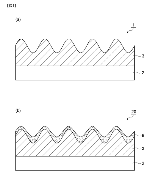
[0020] [Optical substrate]
(a) of Figure 1 is a sectional view schematically illustrating an
optical substrate 1 according to one embodiment. As illustrated in (a)
of Figure 1, the optical substrate 1 according to the present embodiment
comprises a support substrate 2, and a projection-depression structure
layer 3 on a surface of which shapes of projections and depressions are
formed, the projection-depression structure layer being laminated on the
support substrate 2.
[0021] As the support substrate 2, a substrate composed of an inorganic
material such as glass, quartz, or a silicon substrate; a resin substrate
composed of polyethylene terephthalate (PET), polyethylene
naphthalate (PEN), polycarbonate (PC), cycloolefin polymer (COP),
polymethyl methacrylate (PMMA), polystyrene (PS), polyimide (PI),
polyarylate, or the like; and a composite substrate of an inorganic
material and a resin material to enhance gas barrier properties may be
used, for example. Alternatively, for example, gallium arsenic,
sapphire, silicon, silicon nitride, silicon carbide, and zinc oxide can also
8
CA 02935909 2016-07-05
be used for the support substrate 2. The support substrate 2 may be
transparent or may be opaque.
[0022] The support substrate 2 may be surface treated, or an adhesive
layer may be disposed on the support substrate 2 to enhance adhesion.
Moreover, a gas barrier layer may be disposed on the support substrate 2
to prevent invasion of moisture or a gas such as oxygen. Moreover,
the support substrate 2 may have a lens structure having a variety of
optical functions, such as convergence of light and diffusion of light,
and other optical functional layers having a variety of optical functions,
such as convergence of light and diffusion of light, formed on the
surface opposite to the surface on which the projection-depression
structure layer is formed.
[0023] For the projection-depression structure layer 3, sol gel materials
such as silica, Ti-based materials, ITO (indium-tin-oxide)-based
materials, ZnO, Zr02, and A1203 can be used, for example. For
example, in the case where a projection-depression structure layer 3
composed of silica is formed on the support substrate 2 by a sol-gel
method, a sol gel material of a metal alkoxide (silica precursor) is
prepared as an undercoat material. As the precursor of silica,
tetraalkoxide monomers such as tetraalkoxysilanes such as
tetramethoxysilane (TMOS), tetraethoxysilane
(TEOS),
tetra-i-propoxysilane, tetra-n-propoxysilane, tetra-
i-butoxysilane,
tetra-n-butoxysilane, tetra-sec-butoxysilane, and tetra-t-butoxysilane;
trialkoxide monomers such as trialkoxysilanes such as
methyltrimethoxysilane, ethyltrimethoxysilane, propyltrimethoxysilane,
isopropyltrimethoxysilane,
phenyltrimethoxysilane,
9
CA 02935909 2016-07-05
methyltriethoxysilane, ethyltriethoxysi lane,
propyltriethoxysilane,
isopropyltriethoxysilane, phenyltriethoxysilane, methyltripropoxysilane,
ethyltripropoxysilane,
propyltripropoxysilane,
isopropyltripropoxysilane,
phenyltripropoxysilane,
methyltriisopropoxysilane,
ethyltriisopropoxysilane,
propyltriisopropoxysilane,
isopropyltriisopropoxys i lane,
phenyltriisopropoxysilane, and tolyltriethoxysilane; and dialkoxide
monomers such as dialkoxysilanes such as dimethyldimethoxysilane,
dimethyldiethoxysilane,
dimethyldipropoxysilane,
dimethyldiisopropoxysilane, dimethyldi-n-
butoxysilane,
dimethyldi-i-butoxysilane,
dimethyldi-sec-butoxysilane,
dimethyldi-t-butoxysilane,
diethyldimethoxysilane,
diethyldiethoxysilane,
diethyldipropoxysilane,
diethyldiisopropoxysilane,
diethyldi-n-butoxysilane,
diethyldi-i-butoxysilane, diethyldi-sec-
butoxysilane,
diethyldi-t-butoxysilane,
dipropyldimethoxysilane,
dipropyldiethoxysilane,
dipropyldipropoxysilane,
dipropyldiisopropoxysilane,
dipropyldi-n-butoxysilane,
dipropyldi-i-butoxysilane,
dipropyldi-sec-butoxysilane,
dipropyldi-t-butoxysilane,
diisopropyldimethoxysilane,
diisopropyldiethoxysilane,
diisopropyldipropoxysilane,
diisopropyldiisopropoxysilane,
diisopropyldi-n-butoxysilane,
diisopropyldi-i-butoxysilane,
diisopropyldi-sec-butoxysilane,
diisopropyldi-t-butoxysilane,
diphenyldimethoxysilane,
diphenyldiethoxysilane,
diphenyldipropoxysilane,
diphenyldiisopropoxysilane,
diphenyldi-n-butoxysilane,
CA 02935909 2016-07-05
diphenyldi-i-butoxysilane, diphenyldi-sec-
butoxysilane, and
diphenyldi-t-butoxysilane can be used. Furthermore,
alkyltrialkoxysilanes and dialkyldialkoxysilanes contaning alkyl groups
having carbon atoms C4 to C18 can also be used. Metal alkoxides such
as monomers having a vinyl group such as vinyltrimethoxysilane and
vinyltriethoxysilane; monomers having an epoxy group such as
2-(3 ,4-epoxycyclohexyl)ethyltrimethoxysilane,
3 -glycidoxypropylmethyldimethoxysilane,
3 -glycidoxypropyltrimethoxysilane, 3 -
glycidoxypropyl
methyldiethoxysilane, and 3-glycidoxypropyltriethoxysilane; monomers
having a styryl group such as p-styryltrimethoxysilane; monomers
having a methacrylic group such as
3 -methacryloxypropylmethyldimethoxysilane,
3 -methacryloxypropyltrimethoxysilane,
3 -methacryloxypropylmethyldiethoxysilane, and
3-methacryloxypropyltriethoxysilane; monomers having an acrylic
group such as 3-acryloxypropyltrimethoxysilane; monomers having an
amino group such as
N-2-(aminoethyl)-3 -am inopropy lmethy ldimethoxys ilane,
N-2-(aminoethyl)-3 -aminopropyltrimethoxy s i lane,
3 -aminopropyltrimethoxysilane, 3 -
aminopropyltriethoxysilane,
3 -triethoxys ilyl-N-( 1 ,3-dimethyl-butylidene)propylamine, and
N-phenyl-3-aminopropyltrimethoxysilane; monomers having a ureido
group such as 3-ureidopropyltriethoxysilane; monomers having a
mercapto group such as 3-mercaptopropylmethyldimethoxysilane and
3-mercaptopropyltrimethoxysilane; monomers having a sulfide group
11
CA 02935909 2016-07-05
such as bis(triethoxysilylpropyl)tetrasulfide; monomers having an
isocyanate group such as 3 -isocyanatepropyltriethoxysilane; polymers
prepared through polymerization of a small amount of these monomers;
and composite materials comprising a part of the materials listed above
to which a functional group or a polymer is introduced may also be
used. Moreover, part or all of the alkyl group or the phenyl group of
these compounds may be substituted by fluorine. Furthermore,
examples thereof include, but are not limited to, metal acetylacetonate,
metal carboxylate, oxychlorides, chlorides, and mixtures thereof
Examples of metals include, but are not limited to, Ti, Sn, Al, Zn, Zr, In,
in addition to Si, and mixtures thereof. Appropriate mixtures of
precursors of the above-described metal oxides can also be used.
Furthermore, a silane coupling agent having a hydrolyzable group
having affinity and reactivity with silica and a water-repellant organic
functional group in the molecule can be used as a silica precursor.
Examples thereof include silane monomers such as
n-octyltriethoxys i lane,
methyltriethoxysilane, and
methyltrimethoxysilane; vinyl silanes such as vinyltriethoxysilane,
vinyltrimethoxys i lane, vinyltris(2-methoxyethoxy)s i lane, and
vinylmethyldimethoxysilane; methacrylic s i lanes such as
3 -methacryloxypropyltriethoxysilane and
3 -methacryloxypropy ltrimethoxys i lane ; exp oxys i lanes such
as
2-(3 ,4-ep oxycyclohexyl)ethyltrimethoxys i lane,
3 -glyc i doxypropy ltrimethoxys i lane, and
3 -glyc i doxypropyltriethoxys i lane ; mercaptosilanes such
as
3 -mercaptopropy ltrimethoxys i lane and
12
CA 02935909 2016-07-05
3 -merc aptopropyltri ethoxys i lane; sulfur silanes such as
3 -octanoylthio-l-propyltriethoxys il ane ; amino s i lanes such as
3 -aminopropy ltriethoxys i lane, 3 -
aminopropyltrimethoxys ilane,
N-(2-aminoethyl)-3 -am inopropyltrimethoxys i lane,
N-(2-am inoethyl)-3 -aminopropy lmethyldimethoxys i lane, and
3-(N-phenyl)aminopropyltrimethoxysilane; and polymers prepared
through polymerization of these monomers. Moreover, mesoporous
materials may be prepared through addition of a surfactant to these
materials.
[0024] In the cases where a mixture of TEOS and MTES is used as a
solution of a sol gel material, the mixing ratio can be, for example, 1:1
in terms of a molar ratio. In the cases where the sol gel material is
used, hydrolysis and polycondensation reactions are performed to
generate amorphous silica. In the synthetic conditions, an acid such as
hydrochloric acid or an alkali such as ammonia is added to adjust the
pH of the solution. Moreover, a material generating an acid or an
alkali through irradiation with light such as ultraviolet light may be
added. The pH may be 4 or less or 10 or more. Moreover, water may
be added to perform hydrolysis. The amount of water to be added can
be 1.5 times or more the metal alkoxide in terms of the molar ratio.
[0025] Examples of the solvent for the sol gel material solution include
alcohols such as methanol, ethanol, isopropyl alcohol (IPA), and
butanol; aliphatic hydrocarbons such as hexane, heptane, octane,
decane, and cyclohexane; aromatic hydrocarbons such as benzene,
toluene, xylene, and mesitylene; ethers such as diethyl ether,
tetrahydrofuran, and dioxane; ketones such as acetone, methyl ethyl
13
CA 02935909 2016-07-05
ketone, isophorone, and cyclohexanone; ether alcohols such as
butoxyethyl ether, hexyloxyethyl alcohol, methoxy-2-propanol, and
benzyloxy ethanol; glycols such as ethylene glycol and propylene
glycol; glycol ethers such as ethylene glycol dimethyl ether, diethylene
glycol dimethyl ether, and propylene glycol monomethyl ether acetate;
esters such as ethyl acetate, ethyl lactate, and y-butyrolactone; phenols
such as phenol and chlorophenol; amides such as
N,N-dimethylformamide, N,N-dimethylacetamide, and
N-methylpyrrolidone; halogen-based solvents such as chloroform,
methylene chloride, tetrachloroethane, monochlorobenzene, and
dichlorobenzene; hetero element-containing compounds such as carbon
disulfide; water; and mixed solvents thereof Moreover, ethanol and
isopropyl alcohol may be used, or ethanol and isopropyl alcohol may be
mixed with water for use.
[0026] As additives for the sol gel material solution, polyethylene
glycol, polyethylene oxide, hydroxypropyl cellulose, and polyvinyl
alcohol for adjusting viscosity, and solution stabilizers of alkanolamines
such as triethanolamine, 13-diketone such as acetylacetone, P-ketoester,
formamide, dimethylformamide, and dioxane can be used.
[0027] Polysilazane may be used as a material for the
projection-depression structure layer 3. "Polysilazane" indicates a
polymer having a silicon-nitrogen bond, and is a ceramic precursor
inorganic polymer composed of Si-N, Si-H, N-H, and the like, for Si02
and Si3N4 and a solid solution SiOõNy intermediate between 5i02 and
Si3N4, and the like. For example, a compound having a main skeleton
composed of a unit represented by the following formula (1) described
14
CA 02935909 2016-07-05
in Japanese Unexamined Patent Publication No. H8-112879, and
formed into ceramic at a relatively low temperature to be converted into
silica may be used.
formula (1): -Si(R1)(R2)-N(R3)-
In the above formula (1), R', R2, and IV each represent a
hydrogen atom, an alkyl group, an alkenyl group, a cycloalkyl group, an
aryl group, an alkylsilyl group, an alkylamino group, or an alkoxy
group.
[0028] As the material for the projection-depression structure layer 3,
perhydropolysilazane (also referred to as PHPS) or organopolysilazane
can be used, and for example, silicon alkoxide-added polysilazane
obtained through a reaction of polysilazane with silicon alkoxide (for
example, Japanese Unexamined Patent Publication No. H5-238827),
glycidol-added polysilazane obtained through a reaction thereof with
glycidol (for example, Japanese Unexamined Patent Publication No.
H6-122852), alcohol-added polysilazane obtained through a reaction
thereof with alcohol (for example, Japanese Unexamined Patent
Publication No. H6-240208), metal carboxylate-added polysilazane
obtained through a reaction thereof with metal carboxylate (for
example, Japanese Unexamined Patent Publication No. H6-299118),
acetylacetonate complex-added polysilazane obtained through a reaction
thereof with an acetylacetonate complex containing a metal (for
example, Japanese Unexamined Patent Publication No. H6-306329),
and metal nanoparticle-added polysilazane obtained through addition of
metal nanoparticles (for example, Japanese Unexamined Patent
Publication No. H7-196986) can also be used. As an organic solvent
CA 02935909 2016-07-05
for preparing a liquid containing polysilazane, hydrocarbon solvents
such as aliphatic hydrocarbons, alicyclic hydrocarbons, and aromatic
hydrocarbons, halogenated hydrocarbon solvents, and ethers such as
aliphatic ethers and alicyclic ethers can be used. The
organic
polysilazane may be a derivative in which hydrogen sites bonding to Si
are partially substituted with an alkyl group or the like. An amine or a
metal catalyst may also be added to promote conversion into a silicon
oxide compound.
[0029] Moreover, a resin can also be used in the projection-depression
structure layer 3. Examples of curable resins include photocurable,
heat curable, moisture curable, and chemically curable (mixture of two
solutions) resins. Specifically, examples thereof include a variety of
resins such as epoxy, acrylic, methacrylic, vinyl ether, oxetane,
urethane, melamine, urea, polyester, polyolefin, phenol, crosslinked
liquid crystal, fluorine, silicone, and polyamide monomers, oligomers,
and polymers.
[0030] Moreover, the surface of the projection-depression structure
layer 3 may be subjected to hydrophobization. A known method can
be used as a method of hydrophobization. For example, if the surface
of the projection-depression structure layer 3 is a surface composed of
silica, the surface may be hydrophobized with dimethyldichlorosilane,
trimethylalkoxysilane, or the like, or may be hydrophobized with a
trimethylsilylating agent such as hexamethyldisilazane and silicone oil;
or a surface treatment method for metal oxide powder using
supercritical carbon dioxide may be used. Giving hydrophobicity to
the surface of the projection-depression structure layer 3 can readily
16
CA 02935909 2016-07-05
remove moisture from the optical substrate 1 during the process of
manufacturing the device to prevent generation of defects such as dark
spots in the organic EL element or deterioration of the device in the
cases where the optical substrate 1 is used in manufacturing of devices
such as organic EL elements. Moreover, a gas barrier layer may be
disposed on the surface of the projection-depression structure layer 3 to
prevent invasion of moisture or a gas such as oxygen.
[0031] The material for the projection-depression structure layer 3 may
be an inorganic material or a curable resin material containing an
ultraviolet light absorbing material. The ultraviolet light absorbing
material absorbs ultraviolet light and converts light energy into a
harmless form such as heat, thereby demonstrating an action to suppress
deterioration of films. Conventionally known materials can be used as
the ultraviolet light absorbing material; for example,
benzotriazole-based absorbers, triazine-based absorbers, salicylic acid
derivative absorbers, and benzophenone-based absorbers can be used.
[0032] The projection-depression structure layer 3 is formed by
applying the solution or the resin of the sol gel material prepared as
above onto the support substrate 2, and transferring a
projection-depression pattern of the mold for transferring a
projection-depression pattern. The
mold for transferring a
projection-depression pattern and a manufacturing step of transferring a
projection-depression pattern onto the projection-depression structure
layer 3 will be described later.
[0033] Next, the shapes of projections and depressions formed on the
surface of the projection-depression structure layer 3 will be described.
17
CA 02935909 2016-07-05
The shapes of projections and depressions can be analyzed with a
scanning probe microscope (SPM) such as an atomic force microscope
(AFM). In the present embodiment, using a scanning probe
microscope (such as a product name "E-sweep" made by Hitachi
High-Tech Science Corporation), the shapes of projections and
depressions of the projection-depression structure layer 3 are analyzed
on the following analysis conditions to obtain an analyzed image of
projections and depressions and an analyzed image seen in planar view.
In the present specification, the average of distribution of the depth
between a projection and a depression, the standard deviation of the
depth between projections and depressions, the average depth of the
depths between projections and depressions, the average pitch of
projections and depressions, the average of widths of projection
portions, and the proportion of the straight line section and the curved
line section, which are defined below, can be determined by the
following measurement method irrespective of the material of the
surface on which projections and depressions are formed.
<Analysis conditions>
measurement method: intermittent contact method with a cantilever
material for the cantilever: silicon
width of the lever of the cantilever: 40 pm
diameter of the distal end of the chip of the cantilever: 10 nm
[0034] The shapes of projections and depressions formed on the surface
of the projection-depression structure layer 3 in the optical substrate 1
are measured with a scanning probe microscope (such as a product
name "E-sweep" made by Hitachi High-Tech Science Corporation) to
18
CA 02935909 2016-07-05
obtain an analyzed image of projections and depressions. During
analysis of projections and depressions, any measurement region of a 3
wn square (length: 3 m, width: 3 pm) or a 10 lim square (length: 10
[tm, width: 10 1.tm) is measured on the conditions mentioned above to
determine an analyzed image of projections and depressions. At this
time, the data on each depth between a projection and a depression at
measurement points equal to or more than 16384 points (128 points in
length x 128 points in width) within the measurement region is
determined in a scale of nanometer. The number of the measurement
points varies according to the type of the measurement apparatus used
or the setting thereof. For
example, in cases where the
above-mentioned product name "E-sweep" made by Hitachi High-Tech
Science Corporation is used as the measurement apparatus, 65536
points (256 points in length x 256 points in width) can be measured
(measured at a resolution of 256 x 256 pixels) within the measurement
region of a 3 j.im square or a 10 j.tm square. Here, flat processing
including primary inclination correction may be performed on the
analyzed image of projections and depressions to enhance the precision
in measurement.
Moreover, to ensure sufficient precision in
measurement in a variety of analyses related to the shapes of projections
and depressions described below, the measurement region is preferably
a square region having a length of one side 15 times or more the average
of the widths of the projection portions included in the measurement
region.
[0035] The measurement of the depth between a projection and a
depression can be specifically performed as follows. First, among all
19
CA 02935909 2016-07-05
of the measurement points, a measurement point P having the largest
height from the surface of the support substrate 2 is determined. A
plane containing the measurement point P and parallel to the surface of
the support substrate 2 is determined as a reference plane (level plane);
the value of the depth from the reference plane is calculated as the data
on the depth between a projection and a depression. The value of the
depth from the reference plane may be a difference obtained by
subtracting the height of each measurement point from the support
substrate 2 from the value of the height of the measurement point P
from the support substrate 2, for example. Such data on the depth
between a projection and a depression can be determined through
automatic calculation with software or the like in a measurement
apparatus in some measurement apparatuses (such as product name
"E-sweep" made by Hitachi High-Tech Science Corporation).
[0036] After the data on the depth between a projection and a
depression at each measurement point is determined as above, the
calculated values obtained by the arithmetic average and the standard
deviation thereof are used as the average of distribution of the depth
between a projection and a depression and the standard deviation of the
depth between a projection and a depression, respectively.
[0037] The average depth of the depths between projections and
depressions indicates the average of differences in depth when a
difference in depth between a projection portion and a depression
portion on the surface of the projection-depression structure layer 3 on
which projections and depressions are formed (distance in the depth
direction between the vertex portion of a projection portion and the
CA 02935909 2016-07-05
bottom portion of its adjacent depression portion) is measured. Such
an average depth of the depths between projections and depressions can
be calculated by measuring 100 or more distances in the depth direction
between the vertex portions of any projection portions and the bottom
portions of the adjacent depression portions in the analyzed image of
projections and depressions, and determining the arithmetic average.
[0038] The average pitch of projections and depressions indicates the
average of pitches of projections and depressions when pitches of
projections and depressions on the surface of the projection-depression
structure layer 3 on which projections and depressions are formed
(interval between vertex portions of adjacent projection portions or
between bottom portions of adjacent depression portions) are measured.
Such an average pitch of projections and depressions can be calculated
by measuring 100 or more intervals between vertex portions of any
adjacent projection portions or between bottom portions of adjacent
depression portions in the analyzed image of projections and
depressions, and determining the arithmetic average.
[0039] The average pitch of projections and depressions can be within
the range of 100 to 1500 nm, for example, and may further be within the
range of 200 to 1200 nm. The average of distribution of the depth
between a projection and a depression may be within the range of 20 to
200 nm, and may further be within the range of 30 to 150 nm. The
standard deviation of the depth between a projection and a depression
may be within the range of 10 to 100 nm.
[0040] In the present embodiment, a region in which the depth between
a projection and a depression is equal to or more than the average of
21
CA 02935909 2016-07-05
distribution of the depth between a projection and a depression is
defined as a projection portion, while a region in which the depth
between a projection and a depression is less than the average of
distribution of the depth between a projection and a depression is
defined as a depression portion. For example, the analyzed image of
projections and depressions is processed such that the projection
portions are indicated by white, and the depression portions are
indicated by black; thereby, an analyzed image seen in planar view
(monochromatic image) as shown in Figure 2 is obtained. Figure 2 is a
diagram illustrating an example of an analyzed image seen in planar
view of the measurement region in the optical substrate 1 according to
the present embodiment.
[0041] Moreover, the width of the projection portion indicates the width
of projection portion (unit indicated by white) in the analyzed image
seen in planar view. An average of such widths of the projection
portions can be calculated by selecting any 100 or more sites of the
projection portions in the analyzed image seen in planar view,
measuring the length from the boundary of the projection portions to the
opposite boundary in each sites in the direction approximately
orthogonal to the extending direction of the projection portion seen in
planar view, and determining the arithmetic average.
[0042] When the average of the widths of the projection portions is
calculated, the values at places extracted at random from the projection
portion in the analyzed image seen in planar view as described above
are used while the values at branched places of the projection portions
may not be used. Whether or not a region of a projection portion is a
22
CA 02935909 2016-07-05
region related to branching may be determined, for example, by whether
or not the region extends at a predetermined extent or more. More
specifically, it may be determined by whether or not the ratio of the
extending length of the region to the width of the region is a
predetermined value (for example, 1.5) or more.
[0043] Using Figure 3, an example of a method of determining whether
or not a region is branched will be described, the region being projected
in a direction approximately orthogonal to the extended axis line of a
projection portion extending in a direction at an intermediate position of
the projection portion. Here, the extended axis line of the projection
portion indicates a virtual axis line along the extending direction of a
projection portion defined from the shape of the outer edge of the
projection portion where the target region for determination about
branching is excluded from the projection portion. More specifically,
the extended axis line of the projection portion indicates a line drawn
through an approximately midpoint of the width of the projection
portion orthogonal to the extending direction of the projection portion.
(a) of Figure 3 and (b) of Figure 3 are both schematic diagrams for
illustrating an analyzed image seen in planar view in which a projection
portion is partially cut out, and the region S indicates a projection
portion. In (a) of Figure 3 and (b) of Figure 3, regions Al and A2
projected on intermediate positions of projection portions are
determined as targets region for determination about branching. In this
case, when the regions Al and A2 are excluded from the projection
portions, extended axis lines Li and L2 are each defined as a line drawn
through an approximately midpoint of the width of the projection
23
CA 02935909 2016-07-05
portion orthogonal to the extending direction of the projection portion.
Such an extended axis line may be defined by image processing with a
computer, may be defined by an operator who performs analysis, or may
be defined by both image processing with a computer and manual
operation by an operator. In (a) of Figure 3, the region Al is projected
in the direction orthogonal to the extended axis line L 1 at an
intermediate position of the projection portion extending along the
extended axis line L 1 . In (b) of Figure 3, the region A2 is projected in
the direction orthogonal to the extended axis line L2 at an intermediate
position of the projection portion extending along the extended axis line
L2. Based on the same way of thinking as the way of thinking
described below about the regions Al and A2, the regions projected
oblique to the directions orthogonal to the extended axis lines Li and L2
can also be determined whether or not the regions are branched.
[0044] According to the determination method, because the ratio of the
extended length d2 of the region Al to the width dl of the region Al is
approximately 0.5 (less than 1.5), it is determined that the region Al is
not a region related to branching. In this case, the length d3 passing
through the region Al in the direction orthogonal to the extended axis
line L 1 is defined as one of the measurement values for calculating the
average of the widths of the projection portions. In contrast, because
the ratio of the extended length d5 of the region A2 to the width d4 of
the region A2 is approximately 2 (1.5 or more), it is determined that the
region A2 is a region related to branching. In this case, the length d6
passing through the region A2 in the direction orthogonal to the
extended axis line L2 is not defined as one of the measurement values
24
CA 02935909 2016-07-05
for calculating the average of the widths of the projection portions.
[0045] As illustrated in Figure 2, in the optical substrate 1 according to
the present embodiment, the extending directions of the projection
portions (white portions) included in the shapes of projections and
depressions formed on the surface of the projection-depression structure
layer 3 are irregularly distributed seen in planar view. Namely, the
projection portions have shapes extending in irregular directions rather
than regularly aligned stripes or regularly arranged dots. Moreover, in
the measurement region, namely in a predetermined region of the
projection-depression structure layer 3, the outlines of the projection
portions included in a region per unit area seen in planar view include
more straight line sections than curved line sections.
[0046] Figure 4 is a diagram illustrating an example of an analyzed
image seen in planar view of a measurement region in the optical
substrate according to Comparative Example. In the present
embodiment, the term "include more straight line sections than curved
line sections" indicates that the projection-depression pattern intuitively
does not seem like a pattern of the optical substrate according to
Comparative Example illustrated in Figure 4 in which among all of the
sections on the outline of a projection portion, curved line sections
mostly constitute the outline of the projection portion. Whether or not
the outline of the projection portion seen in planar view contains more
straight line sections than curved line sections can be determined by
using one of two methods of defining a curved line section described
below, for example.
[0047] (First method of defining curved line section)
CA 02935909 2016-07-05
In the first method of defining a curved line section, the curved
line section is defined as a section in which a ratio of a linear distance
between both ends of the section to the length of the outline between
both ends of the section is 0.75 or less where a plurality of sections is
formed by dividing the outline of the projection portion seen in planar
view by the length of the average of the widths of the projection portion
multiplied by a factor of TC (circular constant). Moreover, the straight
line section is defined as a section other than the curved line section
among the plurality of sections, namely, a section having the ratio of
more than 0.75. Hereinafter, an example of a procedure to determine
using the first definition method whether or not the outline of a
projection portion seen in planar view contains more straight line
sections than curved line sections will be described with reference to (a)
of Figure 5. (a) of Figure 5 is a diagram illustrating part of an
analyzed image seen in planar view of the projection-depression
structure layer 3, in which depression portions are represented as white
solid portions for convenience. The region Si represents a projection
portion while a region S2 represents a depression portion.
[0048] Procedure 1-1. One projection portion is selected from a
plurality of projection portions in the measurement region. Any
position on the outline X of the projection portion is determined as a
start point. In (a) of Figure 5, Point A is set as a start point as one
example. A reference point is disposed on the outline X of the
projection portion at a predetermined interval from the start point.
Here, the predetermined interval is a length of the average of the widths
of the projection portion multiplied by a factor of (7c (circular
26
CA 02935909 2016-07-05
constant)/2). In (a) of Figure 5, Point B, Point C, and Point D are
sequentially set as one example.
[0049] Procedure 1-2. When Points A to D as reference points are set on
the outline X of the projection portion, the target section for
determination is set. Here, the start point and the end point are
reference points, and sections including the remaining reference points
as intermediate points are set as the targets for determination. In the
example in (a) of Figure 5, if Point A is selected as the start point of a
section, Point C set the second from Point A is the end point of the
section. Here, the interval from Point A is set as the length of the
average of the widths of the projection portion multiplied by a factor of
(n/2), and therefore, Point C is a point located away from Point A along
the outline X by the length of the average of the widths of the projection
portion multiplied by a factor of 7C. Similarly, if Point B is selected as
the start point of a section, Point D set the second from Point B is the
end point of the section. Here, the target section is set in order of the
setting, and assume that Point A is the first set point. Namely, first, the
section between Point A and Point C (section AC) is determined as the
target section for processing. The length La of the outline X of the
projection portion connecting Point A and Point C and the linear
distance Lb between Point A and Point C illustrated in (a) of Figure 5
are then measured.
[0050] Procedure 1-3. Using the length La and the linear distance Lb
measured in Procedure 1-2, the ratio of the linear distance Lb to the
length La (Lb/La) is calculated. If the ratio is 0.75 or less, it is
determined that Point B located as the midpoint of the section AC of the
27
CA 02935909 2016-07-05
outline X of the projection portion is a point present in a curved line
section. In contrast, if the ratio is more than 0.75, it is determined that
Point B is a point present in a straight line section. In the example
illustrated in (a) of Figure 5, the ratio (Lb/La) is 0.75 or less;
accordingly, it is determined that Point B is a point present in a curved
line section.
[0051] Procedure 1-4. Procedure 1-2 and Procedure 1-3 are performed
in cases where the respective points set in Procedure 1-1 are selected as
start points.
[0052] Procedure 1-5. Procedure 1-1 to Procedure 1-4 are performed on
all of the projection portions in the measurement region.
[0053] Procedure 1-6. In cases where among all of the points set for all
of the projection portions in the measurement region, the proportion of
the points determined as points present in straight line sections is 50%
or more of all the points, it is determined that the outline of the
projection portion seen in planar view includes more straight line
sections than curved line sections. In contrast, in cases where among
all of the points set for all of the projection portions in the measurement
region, the proportion of the points determined as points present in
straight line sections is less than 50% of all the points, it is determined
that the outline of the projection portion seen in planar view includes
more curved line sections than straight line sections.
[0054] The processings of Procedure 1-1 to Procedure 1-6 may be
performed using a measurement function included in a measurement
apparatus, by performing software for analysis or the like different from
that included in the measurement apparatus, or manually.
28
CA 02935909 2016-07-05
[0055] The processing of setting points on the outline of the projection
portion in Procedure 1-1 may be terminated when any more point
cannot be set after the setting is done around the projection portion or
when the setting is out of the measurement region. Moreover, because
the ratio (Lb/La) cannot be calculated for sections external to the first
set point and the last set point, these sections are treated as non-targets
for determination. Moreover, projection portions having lengths of the
outlines less than the average of the widths of projection portion
multiplied by a factor of TE are treated as non-targets for determination.
[0056] (Second method of defining curved line section)
In the second method of defining a curved line section, the
curved line section is defined as a section in which among two angles
formed by the line segment (line segment AB) connecting one end of a
segment (Point A) and the midpoint of the section (Point B) and the line
segment (line segment CB) connecting the other end of the section
(Point C) and the midpoint of the section (Point B), the smaller angle
(180 or less) is an angle of 120 or less, where a plurality of sections is
formed by dividing the outline of a projection portion seen in planar
view by the length of the average of the widths of the projection portion
multiplied by a factor of It (circular constant). Moreover, the straight
line section is defined as a section other than the curved line section
among the plurality of sections, namely, a section in which the smaller
angle is more than 120 . Hereinafter, an example of a procedure to
determine using the second definition method whether or not the outline
of a projection portion seen in planar view contains more straight line
sections than curved line sections will be described with reference to (b)
29
CA 02935909 2016-07-05
of Figure 5. (b) of Figure 5 is a diagram illustrating part of an
analyzed image seen in planar view of the same projection-depression
structure layer 3 as that in (a) of Figure 5.
[0057] Procedure 2-1. One projection portion is selected from a
plurality of projection portions in the measurement region. Any
position on the outline X of the projection portion is determined as a
start point. In (b) of Figure 5, Point A is set as a start point as one
example. A reference point is disposed on the outline X of the
projection portion at a predetermined interval from the start point.
Here, the predetermined interval is a length of the average of the widths
of the projection portion multiplied by a factor of (n(circular
constant)/2). In (b) of Figure 5, Point B, Point C, and Point D are
sequentially set as one example.
[0058] Procedure 2-2. When Points A to D as reference points are set on
the outline X of the projection portion, the target section for
determination is set. Here, the start point and the end point are
reference points, and sections including the remaining reference points
as intermediate points are set as the targets for determination. In the
example in (b) of Figure 5, if Point A is selected as the start point of a
section, Point C set the second from Point A is the end point of the
section. Here, the interval from Point A is set as the length of the
average of the widths of the projection portion multiplied by a factor of
(n/2), and therefore, Point C is a point located away from Point A along
the outline X by the length of the average of the widths of the projection
portion multiplied by a factor of 7E. Similarly, if Point B is selected as
the start point of a section, Point D set the second from Point B is the
CA 02935909 2016-07-05
end point of the section. Here, the target section is set in order of the
setting, and assume that Point A is the first set point. Namely, first, the
section between Point A and Point C is determined as the target section
for processing. Among the two angles formed by the line segment AB
and the line segment CB, the smaller angle (180 or less) 0 is then
measured.
[0059] Procedure 2-3. If the angle 0 is 120 or less, it is determined that
Point B is a point present in a curved line section. In contrast, if the
angle 0 is more than 120 , it is determined that Point B is a point
present in a straight line section. In the example illustrated in (b) of
Figure 5, because the angle 0 is 120 or less, it is determined that Point
B is a point present in a curved line section.
[0060] Procedure 2-4. Procedure 2-2 and Procedure 2-3 are performed
in cases where the respective points set in Procedure 2-1 are selected as
start points.
[0061] Procedure 2-5. Procedure 2-1 to Procedure 2-4 are performed on
all of the projection portions in the measurement region.
[0062] Procedure 2-6. In cases where among all of the points set for all
of the projection portions in the measurement region, the proportion of
the points determined as points present in straight line sections is 70%
or more of all the points, it is determined that the outline of the
projection portion seen in planar view includes more straight line
sections than curved line sections. In contrast, in cases where among
all of the points set for all of the projection portions in the measurement
region, the proportion of the points determined as points present in
straight line sections is less than 70% of all the points, it is determined
31
CA 02935909 2016-07-05
that the outline of the projection portion seen in planar view includes
more curved line sections than straight line sections.
[0063] The processings of Procedures 2-1 to 2-6 may be performed
using a measurement function included in a measurement apparatus, by
performing software for analysis or the like different from that included
in the measurement apparatus, or manually.
[0064] The processing of setting points on the outline of the projection
portion in Procedure 2-1 may be terminated when any more point
,
cannot be set after the setting is done around the projection portion or
when the setting is out of the measurement region. Moreover, because
the angle 0 cannot be calculated for sections external to the first set
point and the last set point, these sections are treated as non-targets for
determination. Moreover, projection portions having lengths of the
outlines less than the average of the widths of projection portion
multiplied by a factor of TC are treated as non-targets for determination.
[0065] As described above, it can be determined using one of the first
and second methods of defining a curved line section whether or not the
outline X of a projection portion seen in planar view in a measurement
region includes more straight line sections than curved line sections.
In the projection-depression structure layer 3 of the optical substrate 1,
determination of "whether or not the outline of a projection portion seen
in planar view included in a region per unit area includes more straight
line sections than curved line sections" may be performed based on one
measurement region extracted at random from regions on the surface of
the projection-depression structure layer 3 of the optical substrate 1 and
measured, or may be performed based on comprehensive determination
32
CA 02935909 2016-07-05
of the results in determination of a plurality of different measurement
regions in the same optical substrate 1. In this case, for example,
among the results in determination of a plurality of different
measurement regions, the results having larger number thereof may be
used as the result of determination of "whether or not the outline of a
projection portion seen in planar view included in a region per unit area
includes more straight line sections than curved line sections".
Generation of leak current can be reduced, and light emission efficiency
can be enhanced by forming shapes of projections and depressions on
the surface of the projection-depression structure layer 3 such that the
above-mentioned conditions on the shape are satisfied.
[0066] In the optical substrate 1, the widths of the projection portion in
the direction approximately orthogonal to the extending direction of the
projection portion of the projection-depression structure layer 3 seen in
planar view are constant. Whether or not the widths of the projection
portion are constant or not can be determined based on the widths at 100
or more points of the projection portion obtained by the
above-mentioned measurement. Specifically, from the widths at 100
or more points of the projection portion, the average of the widths of the
projection portion and the standard deviation of the widths of the
projection portion are calculated. The value calculated by dividing the
standard deviation of the widths of the projection portion by the average
of the widths of the projection portion (standard deviation of the width
of the projection portion/average of the widths of the projection portion)
is then defined as the coefficient of variation of the width of the
projection portion. This coefficient of variation has a smaller value as
33
CA 02935909 2016-07-05
the widths of the projection portion are more constant (a fluctuation in
width is smaller). Accordingly, whether or not the widths of the
projection portion are constant can be determined according to whether
or not the coefficient of variation is a predetermined value or less. For
example, it can be defined that the widths of the projection portion are
constant if the coefficient of variation is 0.25 or less. Generation of
leak current can be reduced, and light emission efficiency can be
enhanced by forming shapes of projections and depressions on the
surface of the projection-depression structure layer 3 such that the
above-mentioned conditions on the shape are satisfied.
[0067] In the following description, a condition indicating that the
proportion of the straight line section determined by the first definition
method is 50% or more (or proportion of the straight line section
determined by the second definition method is 70% or more) is referred
to as "straight line condition", and a condition indicating that the
coefficient of variation of the width of the projection portion is 0.25 or
less is referred to as "width condition".
[0068] In cases where in the optical substrate 1, an analyzed image of
projections and depressions obtained through analysis, with a scanning
probe microscope, of the shapes of projections and depressions formed
on the surface of the projection-depression structure layer 3 is subjected
to two-dimensional high-speed Fourier transformation to obtain a
Fourier transformed image, the Fourier transformed image shows a
circular pattern or an annular pattern in which the origin having the
absolute value of a wavenumber of 0 1.tm-1 is approximately in the
center, and the circular pattern or the annular pattern may be present
34
CA 02935909 2016-07-05
within the region having an absolute value of a wavenumber within the
range of 10 p.m' or less (may be within the range of 0.667 to 10 JAM- 1 ,
or may further be within the range of 0.833 to 5 lim-1). If shapes of
projections and depressions are formed on the surface of the
projection-depression structure layer 3 such that the above conditions
(hereinafter, referred to as "FFT condition") are satisfied, the
wavelength dependency of light emission and the orientation (properties
of light intensely emitting in a predetermined direction) can be
sufficiently reduced.
[0069] The term "a circular pattern or an annular pattern of a Fourier
transformed image" indicates a pattern observed as a result of gathering
of bright points in the Fourier transformed image. For this reason, the
term "circular" here indicates that the pattern composed of gathering
bright points looks approximately circular, and the concept includes a
pattern whose outer shape partially looks like projections or
depressions. Moreover, the term "annular" indicates that the pattern
composed of gathering bright points looks approximately annular, is the
concept including a pattern of an annular shape whose outer circle
and/or inner circle looks approximately circular, and partially looks
projected or depressed. Moreover, the term "the circular pattern or the
annular pattern is present within the region having an absolute value of
a wavenumber within the range of 10 1.1m-1 or less (may be within the
range of 0.667 to 10 prm-1, or may further be within the range of 0.833 to
5 [tm-1)" indicates that among the bright points forming a Fourier
transformed image, 30% or more of the bright points is present within a
region having an absolute value of a wavenumber within the range of 10
CA 02935909 2016-07-05
vim-1 or less (may be within the range of 0.667 to 10 1.1,m-1, or may
further be within the range of 0.833 to 5 pin-').
[0070] The followings are found about the relation between the pattern
of the projection-depression structure and a Fourier transformed image.
If the projection-depression structure itself does not have any
distribution of the pitch or any orientation thereof, the Fourier
transformed image also appears as a random pattern (no pattern); if the
projection-depression structure, as a whole, is isotropic in the X and Y
directions but has distribution of the pitch, a circular or annular Fourier
transformed image appears. Moreover, if the projection-depression
structure has a single pitch, the annular shape appearing in the Fourier
transformed image tends to be sharp.
[0071] The Fourier transformed image is obtained as follows: the
shapes of projections and depressions formed on the surface of the
projection-depression structure layer 3 are analyzed with a scanning
probe microscope (such as a product name "E-sweep" made by Hitachi
High-Tech Science Corporation) to obtain an analyzed image of
projections and depressions, and then, the analyzed image of projections
and depressions is subjected to two-dimensional high-speed Fourier
transformation. The two-dimensional high-speed Fourier
transformation of the analyzed image of projections and depressions can
be easily performed by electronic image processing using a computer
including software for two-dimensional high-speed Fourier
transformation.
[0072] [Method of manufacturing optical substrate]
Next, a method of manufacturing the above-mentioned optical
36
CA 02935909 2016-07-05
substrate I will be described. The
optical substrate 1 can be
manufactured as follows, for example. First, while a film-shaped mold
having a projection-depression pattern formed thereon is being
pressed against an undercoat material layer 4 formed by applying a so!
5 gel material, as a material for a projection-depression structure layer
3,
on a support substrate 2, the undercoat material layer 4 is hardened.
Subsequently, the film-shaped mold 5 is removed from the undercoat
material layer 4 after hardening (projection-depression structure layer
3). Hereinafter, the film-shaped mold 5 and the above steps will be
described in detail using Figure 6.
[0073] As illustrated in Figure 6, the film-shaped mold 5 includes a
substrate portion 5a, and a projection-depression portion 5b formed on
the substrate portion 5a. The
substrate portion 5a and the
projection-depression portion 5b both have flexibility. A
projection-depression pattern is preliminarily formed on the surface of
the projection-depression portion 5b through transfer of the
projection-depression pattern from a metal mold 8 described later. The
substrate portion 5a is in the form of a film or a sheet, and is formed of
an organic material such as a silicone resin, polyethylene terephthalate
(PET), polyethylene terenaphthalate (PEN), polycarbonate (PC), a
cycloolefin polymer (COP), polymethyl methacrylate (PMMA),
polystyrene (PS), polyimide (PI), or polyarylate, for example.
Moreover, the projection-depression portion 5b may be formed of the
same material as that for the substrate portion 5a to be formed integrally
with the substrate portion 5a, or a different material may be used. As a
material for forming the projection-depression portion 5b, a
37
CA 02935909 2016-07-05
photocurable resin, a heat curable resin, a thermoplastic resin, or the like
can be used. Moreover, the substrate portion 5a may be surface
treated, or an easily-adhesive layer may be disposed on the substrate
portion 5a to enhance adhesion; or a gas barrier layer may be disposed
on the substrate portion 5a to prevent invasion of moisture or a gas such
as oxygen.
[0074] The dimension of the film-shaped mold 5, particularly the length
thereof can be appropriately set according to the dimension of the
optical substrate 1 to be mass produced or the number of the optical
substrate 1 continuously manufactured in a single manufacturing
process (the number of lots). For example, a long mold having a
length of 10 m or more may be used to continuously transfer a pattern to
a plurality of substrates while a film-shaped mold 5 wound around a roll
is being continuously fed from the roll. The width of the film-shaped
mold 5 can be 50 to 3000 mm, and the thickness thereof can be 1 to 500
lam. A surface treatment or a treatment facilitating adhesion may be
performed between the substrate portion 5a and the
projection-depression portion 5b to enhance adhesion. Moreover, the
surface of the projection-depression pattern of the projection-depression
portion 5b may be subjected to a release treatment when necessary.
[0075] As illustrated in Figure 6, the film-shaped mold 5 is fed between
a pressurizing roll 6 and the support substrate 2 conveyed immediately
under the film-shaped mold 5 to transfer the projection-depression
pattern of the projection-depression portion 5b in the film-shaped mold
5 onto the undercoat material layer 4 on the support substrate 2. Here,
after the film-shaped mold 5 is pressed against the undercoat material
38
CA 02935909 2016-07-05
layer 4, the undercoat material layer 4 may be pre-calcinated. Gelation
of the undercoat material layer 4 progresses through pre-calcination to
solidify the projection-depression pattern, so that the
projection-depression pattern is barely damaged during releasing. In
cases where pre-calcination is performed, the undercoat material layer 4
may be heated at a temperature of 40 to 150 C in the air.
Pre-calcination does not always need to be performed.
[0076] After pressurizing of film-shaped mold 5 or pre-calcination of
the undercoat material layer 4, the film-shaped mold 5 is released from
the undercoat material layer 4. A known releasing method can be used
in releasing of the film-shaped mold 5. For example, the film-shaped
mold 5 may be released while being heated. Thereby, a gas generated
from the undercoat material layer 4 can be escaped to prevent
generation of air bubbles in the undercoat material layer 4. In cases
where a roll process is used, a peel force may be smaller than that in a
plate-shaped mold used in a press method, and the film-shaped mold 5
can be readily released from the undercoat material layer 4 without the
undercoat material layer 4 remaining on the film-shaped mold 5.
Particularly, because the undercoat material layer 4 is pressurized while
being heated, the reaction readily progresses, and the film-shaped mold
5 is readily released from the undercoat material layer 4 immediately
after pressurizing. Furthermore, a release roll 7 may be used to
enhance the releasing properties of the film-shaped mold 5. In the
present embodiment, as illustrated in Figure 6, a release roll 7 is
disposed downstream of the pressurizing roll 6 to rotatably support the
film-shaped mold 5 while the film-shaped mold 5 is being urged against
39
CA 02935909 2016-07-05
the undercoat material layer 4 with the release roll 7. Thereby, a state
where the film-shaped mold 5 is applied to the undercoat material layer
4 can be maintained by the distance between the pressurizing roll 6 and
the release roll 7 (for a predetermined period of time). The traveling
direction of the film-shaped mold 5 is then changed downstream of the
release roll 7 so as to draw the film-shaped mold 5 upward from the
release roll 7. Thereby, the film-shaped mold 5 is peeled off from the
undercoat material layer 4 in which projections and depressions are
formed. The above-mentioned pre-calcination of the undercoat
material layer 4 or heating may be performed during the period of time
in which the film-shaped mold 5 is applied to the undercoat material
layer 4. In cases where the release roll 7 is used, releasing of the mold
50 can be further facilitated through releasing while heating to, for
example, 40 to 150 C is being performed.
[0077] After the film-shaped mold 5 is released from the undercoat
material layer 4, the undercoat material layer 4 may be hardened.
Thereby, a projection-depression structure layer 3 having a
projection-depression pattern as illustrated in Figure 1 is formed. In
the present embodiment, the undercoat material layer 4 composed of the
sol gel material can be hardened by main calcination. Hydroxyl
groups and the like contained in silica (amorphous silica) forming the
undercoat material layer 4 are removed by main calcination, thereby the
strength of the undercoat material layer 4 is increased. Main
calcination is preferably performed at a temperature of 200 to 1200 C
for about 5 minutes to 6 hours. The undercoat material layer 4 is thus
hardened to form a projection-depression structure layer 3 having a
CA 02935909 2016-07-05
projection-depression pattern corresponding to the
projection-depression pattern of the film-shaped mold 5. At this time,
if the projection-depression structure layer 3 is composed of silica, the
projection-depression structure layer 3 becomes amorphous, crystalline,
or a mixed state of amorphous and crystalline states according to the
calcination temperature and the calcination time.
[0078] Moreover, a material generating an acid or an alkali through
irradiation with light such as ultraviolet light may be added to the
undercoat material layer 4. Moreover, when the projection-depression
pattern of the projection-depression portion 5b of the film-shaped mold
5 is transferred onto the undercoat material layer 4 on the support
substrate 2, the undercoat material layer 4 may be photocured through
irradiation with energy beams such as UV or excimer UV to
manufacture the optical substrate 1. Moreover, a gas barrier layer may
be disposed on the surface of the projection-depression structure layer 3
to prevent invasion of moisture or a gas such as oxygen.
[0079] [Method of manufacturing film-shaped mold]
Next, the method of manufacturing the film-shaped mold 5 will
be described. To produce a film-shaped mold 5, a master pattern for
forming a projection-depression pattern on a mold is first produced.
The master projection-depression pattern may be formed, for example,
by a method using self-organization through heating of a block
copolymer (microphase separation) (hereinafter, appropriately referred
to as "BCP (Block Copolymer) heat annealing method") described in
W02012/096368 by the present applicants, or by a method using
self-organization of a block copolymer under a solvent atmosphere
41
CA 02935909 2016-07-05
(hereinafter, appropriately referred to as "BCP solvent annealing
method") disclosed in W02011/007878 Al by the present applicants.
The master projection-depression pattern may be formed by
photolithography instead of the BCP heat annealing method and the
BCP solvent annealing method. Besides, the
master
projection-depression pattern can also be produced, for example, by
machining, microfabrication methods such as an electron beam direct
drawing method, a corpuscular beam processing method, and an
operation probe processing method, and microfabrication methods using
self-organization of nanoparticles. If the pattern is formed by the BCP
heat annealing method, any material can be used as a material for
forming a pattern. For example, the material may be a block
copolymer composed of a combination of two materials selected from
the group consisting of styrene polymers such as polystyrene, polyalkyl
methacrylate such as polymethyl methacrylate, polyethylene oxide,
polybutadiene, polyisoprene, polyvinylpyridine, and polylactic acid.
[0080] The BCP solvent annealing method is a method of solvent
annealing (solvent phase separation) a thin film of a block copolymer
applied onto a substrate and dried under an atmosphere of a steam of an
organic solvent and forming a phase separated structure of the block
copolymer inside the thin film instead of performing the first heating
step, the etching step, and the second heating step in the BCP heat
annealing method described in W02012/096368. Self-organization of
the block copolymer progresses through this solvent annealing, so that
the block copolymer can be subjected to microphase separation and a
projection-depression structure can be formed.
42
CA 02935909 2016-07-05
[0081] Solvent annealing can be performed, for example, by generating
an atmosphere of steam of an organic solvent inside the air-tight
container like a desiccator, and exposing a thin film of a block
copolymer as a target product to the atmosphere. The steam of the
organic solvent may have a high concentration to promote phase
separation of the block copolymer. Moreover, the steam of the organic
solvent may have a saturated vapor pressure. In this case, control of
the concentration is also relatively easy. For example, if the organic
solvent is chloroform, it is known that the quantity of saturated steam is
0.4 g/1 to 2.5 g/1 at room temperature (0 C to 45 C). The treatment
time by solvent annealing may be 6 hours to 168 hours, 12 hours to 48
hours, or 12 hours to 36 hours.
[0082] The organic solvent used in solvent annealing may be an organic
solvent having a boiling point of 20 C to 120 C. For example,
chloroform, dichloromethane, toluene, tetrahydrofuran (THF), acetone,
carbon disulfide, and mixed solvents thereof can be used. Among
these solvents, chloroform, dichloromethane, acetone, and a mixed
solvent of acetone/carbon disulfide may be used. The temperature of
the atmosphere during solvent annealing may be within the range of 0 C
to 45 C. If the temperature of the atmosphere during solvent
annealing is higher than 45 C, a projection-depression structure to be
formed on a thin film is softened and readily damaged. The organic
solvent barely evaporates in environments at a temperature lower than
0 C, so that phase separation of the block copolymer is barely caused.
[0083] The projection-depression structure of the thin film obtained by
the solvent annealing described above may be subjected to a heat
43
CA 02935909 2016-07-05
treatment. Because the projection-depression structure is already
formed by solvent annealing, the projection-depression structure already
formed is smoothed by this heat treatment, although the heat treatment
is not always needed. The heat treatment may be effective if
protrusions are generated on part of the surface of the
projection-depression structure after solvent annealing for some reasons,
or may be effective in adjusting the period or the height of the
projection-depression structure. The heating temperature can be set at
a temperature equal to or higher than the glass transition temperature of
the polymer segment forming the block copolymer, for example, and
can be set at a temperature equal to or higher than the glass transition
temperature of the homopolymer thereof and equal to or lower than a
temperature 70 C higher than the glass transition temperature, for
example. The heat treatment can be performed in the air atmosphere
using an oven or the like. After solvent annealing is performed,
etching may be performed by a dry etching such as an etching of
irradiation with an energy beam which is an UV, excimer UV, or the
like, or like RIE (reactive ion etching). Moreover, a heat treatment
may be further performed.
[0084] A metal mold having a projection-depression pattern further
transferred by electrocasting or the like can be formed after the master
projection-depression pattern is formed by the BCP heat annealing
method, the BCP solvent annealing method, or the like. First, a seed
layer serving as a conductive layer for electrocasting can be formed on
the master having the pattern by non-electrolytic plating, sputtering,
deposition, and the like. The thickness of the seed layer may be 10 nm
44
CA 02935909 2016-07-05
or more to provide a uniform current density in the subsequent
electrocasting step and provide a constant thickness of a metal layer
deposited in the subsequent electrocasting step. As a material for the
seed layer, nickel, copper, gold, silver, platinum, titanium, cobalt, tin,
zinc, chromium, gold-cobalt alloys, gold-nickel alloys, boron-nickel
alloys, solder, copper-nickel-chromium alloys, tin nickel alloys,
nickel-palladium alloys, nickel-cobalt-phosphorus alloys, and alloys
thereof can be used, for example. Next, a metal layer is deposited on
the seed layer through electrocasting (electric field plating). The total
thickness of the metal layer including the thickness of the seed layer can
be a thickness of 10 to 3000 m, for example. As a material for the
metal layer deposited through electrocasting, any of the metals listed
above and used in the seed layer can be used. It is desired that the
formed metal layer have appropriate hardness and thickness in view of
facilitating the subsequent treatments such as pressing of the
film-shaped mold 5 to the projection-depression portion 5b, releasing,
and washing.
[0085] The metal layer including the seed layer thus obtained is
released from the master having a projection-depression structure and a
metal substrate is obtained. Releasing of the metal layer may be
physically performed, or the materials for forming a pattern may be
dissolved in an organic solvent which dissolves these, such as toluene,
tetrahydrofuran (THF), or chloroform to be removed. When the metal
substrate is released from the master, the remaining material
components can be removed by washing. As a washing method, wet
washing using a surfactant or the like or dry washing using ultraviolet
CA 02935909 2016-07-05
light, plasma, or the like can be used. Moreover, the remaining
material components may be removed through adhesion to a
pressure-sensitive adhesive or an adhesive, for example. A metal
substrate having a pattern transferred from the master is thereby
obtained.
[0086] The metal substrate may be formed into a roll with the
projection-depression pattern facing toward the outside. Thereby, as
illustrated in Figure 7, a cylindrical metal mold 8 having a
projection-depression portion 8a formed along the outer periphery is
obtained. Here, the projection-depression pattern formed in the
projection-depression portion 8a is a projection-depression pattern
formed through microphase separation of a block copolymer by a BCP
heat annealing method, a BCP solvent annealing method, or the like as
described above, and is a projection-depression pattern corresponding to
the shapes of projections and depressions formed on the
projection-depression structure layer 3 of the optical substrate 1. In
Figure 7, the detailed illustration of the projection-depression pattern
formed on the projection-depression portion 8a is omitted.
[0087] Subsequently, a method of producing the film-shaped mold 5 by
transferring the projection-depression pattern of the metal mold 8 will
be described. After a curable resin is applied onto the substrate portion
5a and a resin layer (serving as a projection-depression portion 5b) is
formed on the substrate portion 5a, the resin layer is hardened while the
projection-depression portion 8a of the metal mold 8 is being pressed
against the resin layer. Here, as the curable resin, a variety of resins
such as epoxy, acrylic, methacrylic, vinyl ether, oxetane, urethane,
46
CA 02935909 2016-07-05
melamine, urea, polyester, phenol, crosslinked liquid crystal, fluorine,
and silicone resins can be used. As a method of applying a curable
resin onto the substrate portion 5a, a variety of coating methods such as
spin coating, spray coating, dip coating, dropping, gravure printing,
screen printing, relief printing, die coating, curtain coating, inkjet
process, and sputtering can be used, for example. Furthermore,
although the conditions for hardening the curable resin vary according
to the type of the resin to be used, the curing temperature may be within
the range of room temperature to 250 C, and the curing time may be
within the range of 0.5 minutes to 3 hours, for example. Moreover, a
method of hardening the resin through irradiation with energy beams
such as ultraviolet light or electron beams may be used; in this case, the
irradiation intensity may be within the range of 20 mJ/cm2 to 5 J/cm2.
[0088] Next, the metal mold 8 is removed from the resin layer after
hardening. The method of removing the metal mold 8 is not limited to
a mechanical releasing method, and a known method can be used. A
film-shaped mold 5 in which a projection-depression portion 5b having
projections and depressions formed thereon is formed on the substrate
portion 5a is thereby obtained. The film-shaped mold 5 can also be
used as an optical substrate in the form of a film.
[0089] As illustrated in (b) of Figure 1, a coating layer 9 may be formed
on the projection-depression structure layer 3 in the optical substrate 1.
Thereby, an optical substrate 20 is manufactured in which the coating
layer 9 is formed in a film thickness within the range of 25 to 150% of
the standard deviation of the depth between a projection and a
depression in the projection-depression structure layer 3. According to
47
CA 02935909 2016-07-05
the optical substrate 20, if foreign substances or defects are present on
the surface of the projection-depression structure layer 3, these can be
covered with the coating layer 9. In cases where the optical substrate
20 having the coating layer 9 formed thereon is used as a substrate for
an organic EL element, the resulting organic EL element has good
out-coupling efficiency, and the leak current thereof can be effectively
suppressed. Accordingly, the optical substrate 20 having the coating
layer 9 formed thereon is effective as a member used in a variety of
devices such as organic EL elements.
[0090] As the material for the coating layer 9 (coating material),
materials used for the projection-depression structure layer 3, the same
sol gel materials as those used for the undercoat material layer 4,
polysilazane, curable resins, and the like can be used.
[0091] As the coating material, inorganic materials such as Ti02, ZnO,
ZnS, ZrO, BaTiO3, and SrTiO2 may be used. Among these inorganic
materials, TiO2 may be used in relation to film forming properties and
the refractive index. The coating layer 9 can be formed by any
method; a method of applying a solution of a sol gel material for
gelation, a method of applying an inorganic nanoparticle dispersion
liquid and drying the liquid, liquid phase deposition (LPD: Liquid Phase
Deposition), and the like can be used. If a dispersion liquid of TiO2 is
used, a sol-gel method of applying a sol gel solution using alkoxide of
titanium or an organic compound thereof by spin coating or the like, and
gelating the solution through drying with heating may be used.
[0092] Moreover, a silane coupling agent may be used as the coating
material. If an organic EL element is manufactured using the optical
48
CA 02935909 2016-07-05
substrate 20 having the projection-depression structure layer 3, the
adhesion between the coating layer 9 and a layer to be formed thereon
such as an electrode can be thereby enhanced, and resistance in the
washing step and the treatment step at high temperature in the
manufacturing process of the organic EL element can be improved.
The type of the silane coupling agent used in the coating layer 9 is not
particularly limited. As such a silane coupling agent, an organic
compound represented by RSiX3 can be used, for example. R is an
organic functional group containing at least one group selected from the
group consisting of a vinyl group, a glycidoxy group, an acrylic group, a
methacrylic group, an amino group, and a mercapto group; X is a
halogen element or an alkoxyl group. As the method of applying the
silane coupling agent, a variety of coating methods such as spin coating,
spray coating, dip coating, dropping, gravure printing, screen printing,
relief printing, die coating, curtain coating, inkjet process, and
sputtering can be used, for example. Subsequently, the coating can be
dried on an appropriate condition according to the materials and a
hardened film can be obtained. For example, the coating may be dried
with heating at 100 to 150 C for 15 to 90 minutes.
[0093] Moreover, the surface of the coating layer 9 may be subjected to
hydrophobization. As the hydrophobization method, a known method
may be used; for example, if the surface of the coating layer 9 is a
surface composed of silica, the surface can be hydrophobized with
dimethyldichlorosilane, trimethylalkoxysilane, or the like; a method of
hydrophobizing the surface with a trimethylsilylating agent such as
hexamethyldisilazane and silicone oil; a method of surface treating
49
CA 02935909 2016-07-05
metal oxide powder using supercritical carbon dioxide may be used.
Giving hydrophobicity to the surface of the coating layer 9 can readily
remove moisture from the optical substrate 20 during the manufacturing
process in cases where the optical substrate 20 is used in manufacturing
of devices such as organic EL elements. Thereby, generation of
defects such as dark spots in the organic EL element or deterioration of
devices can be prevented.
[0094] The undercoat material and/or the coating material may be an
inorganic material or a curable resin material containing an ultraviolet
light absorbing material. The ultraviolet light absorbing material
absorbs ultraviolet light and converts light energy into a harmless form
such as heat, thereby demonstrating an action to suppress deterioration
of films. Conventionally known materials can be used as the
ultraviolet light absorbing material; for example, benzotriazole-based
absorbers, triazine-based absorbers, salicylic acid derivative absorbers,
and benzophenone-based absorbers can be used.
[0095] [Organic EL element]
(a) of Figure 8 is a sectional view schematically illustrating an
example (organic EL element 100) of an organic EL element (light
emitting element) using the optical substrate 1 as a diffraction grating
substrate. (b) of Figure 8 is a sectional view schematically illustrating
an example (organic EL element 200) of an organic EL element (light
emitting element) using an optical substrate 20 as a diffraction grating
substrate.
[0096] As a method of laminating an organic layer 11, a known method
such as deposition, sputtering, spin coating, or die coating can be
CA 02935909 2016-07-05
appropriately used. As illustrated in (a) of Figure 8, in the organic EL
element 100, a support substrate 2, a projection-depression structure
layer 3, a first electrode 10, an organic layer 11, and a second electrode
12 are laminated in this order such that the shapes of projections and
depressions formed on the surface of the projection-depression structure
layer 3 are maintained in these layers.
[0097] In contrast, as illustrated in (b) of Figure 8, in cases where a
coating layer 9 is formed on the projection-depression structure layer 3
by a conventionally known application method, a solution for forming
the coating layer 9 is readily accumulated on the depression portions of
the surface of the projection-depression structure layer 3, and therefore
the resulting shape of the coating layer 9 is shapes of projections and
depressions milder than the shapes of the projections and depressions of
the projection-depression structure layer 3. The first electrode 10, the
organic layer 11, and the second electrode 12 formed on the coating
layer 9 are formed such that the shapes of projections and depressions
formed on the surface of the coating layer 9 are maintained in these
layers.
[0098] It should be noted that in both of these cases described above,
the surface of the organic layer 11 may be formed to have a shape
milder than the projection-depression pattern formed on the surface of
the projection-depression structure layer 3 or the coating layer 9.
Moreover, the surface may be flat. Similarly, the surface of the second
electrode 12 laminated on the organic layer 11 may be formed to have a
shape milder than the projection-depression pattern formed on the
organic layer 11, or may be flat. For example, in cases where the
51
CA 02935909 2016-07-05
organic layer 11 is formed by a conventionally known application
method, the shape of the organic layer 11 is shapes of projections and
depressions even milder than the shapes of projections and depressions
of the first electrode 10.
[0099] The first electrode 10 has transmissive property to transmit light
from the organic layer 11 formed thereon to the optical substrate 1.
Accordingly, the first electrode 10 is also referred to as transparent
electrode. As an electrode material, indium oxide, zinc oxide, tin
oxide, composites thereof, i.e., indium-tin-oxide (ITO), gold, platinum,
silver, and copper are used, for example. Among these materials, ITO
may be used in view of transparency and conductivity. The organic
layer 11 is not particularly limited as long as it can be used as an organic
layer of an organic EL element, and a known organic layer can be
appropriately used. As a material for the second electrode 12, a
substance having a small work function can be appropriately used, and
examples thereof include, but are not particularly limited to, aluminum,
MgAg, MgIn, and AlLi.
[0100] A modification (organic EL element 300) of the organic EL
element 100 is illustrated in Figure 9. The organic EL element 300
uses an optical substrate 30 having an optical functional layer 13
disposed on the outer surface (surface opposite to the surface on which
the projection-depression structure layer 3 is formed) of the support
substrate 2 as diffraction grating. Total reflection of the light passing
through the support substrate 2 at the interface between the support
substrate 2 (including the optical functional layer 13) and air can be
suppressed through disposition of such an optical functional layer 13
52
CA 02935909 2016-07-05
and out-coupling efficiency can be enhanced. As the optical functional
layer 13, a hemispherical lens or a corrugated structure lens (microlens
described in Japanese Unexamined Patent Publication No.
2011-243308) can be used, for example. The optical functional layer
13 can be any optical functional layer which can be used for extraction
of light from the organic EL element 300 and is not particularly limited;
any optical member having a structure which can control refraction,
convergence, diffusion (scattering), diffraction, reflection, and the like
of light to extract light to the outside of the element can be used. As
the optical functional layer 13, a variety of lens members such as a
convex lens like a hemispherical lens, a concave lens, a prism lens, a
cylindrical lens, a lenticular lens, and a microlens composed of a
projection-depression layer having a corrugated structure which can be
formed by the same method as the above-mentioned method of
manufacturing the optical substrate 1 can be used, for example.
Moreover, as the optical functional layer 13, a diffusion sheet or plate in
which a diffusion material is kneaded into a transparent substance may
be used; a diffusion sheet or plate having a projection-depression
structure on the surface thereof, a diffraction grating, and a member
having an anti-reflective function may be used. Among these
members, a lens member may be used because the lens member can
more efficiently extract light. Moreover, as these lens members, a
plurality of lens members may be used; in this case, fine lens members
may be aligned to form a so-called microlens (array). As the optical
functional layer 13, commercially available products may be used.
[0101] Moreover, as such an optical functional layer 13 for extracting
53
CA 02935909 2016-07-05
light to the outside, those having a variety of sizes and shapes can be
used according to, for example, the applications of the organic EL
element or the size and the configuration of the organic EL element;
from the viewpoint of suppressing reflection at the interface between the
air and the external extracting structure, a microlens composed of a
projection-depression layer having a corrugated structure which can be
formed by the same method as the method of manufacturing a
hemispherical lens and a diffraction grating substrate described later
may be used. Furthermore, in cases where the thickness of the organic
EL element is not important (thickness thereof may be large), a
hemispherical lens may be used as the optical functional layer 13.
Moreover, in cases where the thickness is important (thin organic EL
element is preferred), a microlens composed of the
projection-depression layer having a corrugated structure or a Fresnel
lens may be used as the optical functional layer 13. The optical
functional layer 13 is used as a role of a lens for mainly controlling
refraction of light, but is not limited to this; the optical functional layer
13 can also be used as a layer for giving a variety of optical properties
such as convergence, diffusion (scattering), diffraction, and prevention
of reflection of light.
[0102} The material for such an optical functional layer 13 is not
particularly limited, and an optical member composed of any material
can be used. As the optical functional layer 13, transparent inorganic
materials such as glass, and transparent resin materials composed of
transparent polymers like polyester resins such as polyethylene
terephthalate, cellulose resins, acetate resins, polyether sulfone resins,
54
CA 02935909 2016-07-05
polycarbonate resins, polyamide resins, polyimide resins, polyolefin
resins, acrylic resins, and the like can be used, for example. Moreover,
the optical functional layer 13 may be laminated on the support
substrate 2 with the pressure-sensitive adhesive layer and/or adhesive
layer being interposed therebetween so as not to contain the air between
the organic EL element and the optical functional layer 13 to suppress
reflection between the organic EL element and the optical functional
layer 13.
[0103] Furthermore, from the viewpoint of enhancing friction
resistance and scratch resistance of the surface of the optical functional
layer 13, the optical functional layer 13 may have a protective layer
laminated on the surface of the optical member (on the surface on which
the shapes of projections and depressions are formed, in cases where a
microlens composed of a projection-depression layer described above is
used as the optical functional layer 13). As such a protective layer, a
transparent film or a transparent inorganic deposition layer can be used.
Such a transparent film is not particularly limited, and any transparent
film can be used; examples thereof include films composed of
transparent polymers like polyester resins such as polyethylene
terephthalate, cellulose resins, acetate resins, polyether sulfone resins,
polycarbonate resins, polyamide resins, polyimide resins, polyolefin
resins, acrylic resins, and the like. Moreover, in such a transparent
film, a pressure-sensitive adhesive layer or an adhesive layer may be
formed on one surface thereof, and this transparent film may be bonded
to the surface of the optical member and used (in cases where a
microlens composed of a projection-depression layer described above is
CA 02935909 2016-07-05
used as the optical functional layer 13, the transparent film may be
bonded so as to form a space between projection portions). As such a
pressure-sensitive adhesive or an adhesive, acrylic pressure-sensitive
adhesives, ethylene-vinyl acetate copolymers, natural rubber
pressure-sensitive adhesives, synthetic rubber pressure-sensitive
adhesives composed of polyisobutylene, butyl rubber,
styrene-butylene-styrene copolymers, styrene-isoprene-styrene block
copolymers, and the like, polyurethane pressure-sensitive adhesives, and
polyester pressure-sensitive adhesives may be used, for example.
[0104] Moreover, in cases where an inorganic deposition layer is
laminated as the protective layer, known metal materials which can be
formed into a transparent inorganic layer by deposition can be
appropriately used; examples thereof include oxides, nitrides, sulfides of
metals such as Sn, In, Te, Ti, Fe, Co, Zn, Ge, Pb, Cd, Bi, Se, Ga, and
Rb. Moreover, TiO2 can be suitably used as such a metal material
from the viewpoint of sufficiently preventing deterioration due to
oxidation, or ZnS can be suitably used from the viewpoint of attaining
high luminance at low cost. Moreover, the method of forming such an
inorganic deposition layer is not particularly limited, and the inorganic
deposition layer can be appropriately manufactured by any physical
deposition apparatus.
[0105] The organic EL elements 100 and 200 using the optical
substrates 1 and 20 as diffraction grating substrates and the bottom
emitting organic EL element 200 using the optical substrate 30 as a
diffraction grating substrate have been described. However, the
application of the optical substrates 1, 20, and 30 is not limited to the
56
CA 02935909 2016-07-05
diffraction grating substrate of the bottom emitting organic EL element.
The optical substrates 1, 20, and 30 can also be used, for example, in
manufacturing of optical elements such as top emitting organic EL
elements, LEDs, LECs, ECLs, solar cells, microlens arrays, prism
arrays, and optical waveguides, optical parts such as lenses,
anti-reflection films, viewing angle improving films, semiconductor
chips, patterned media, data storages, electronic paper, LSIs, and the
like, and can be applied to anti-fogging substrates, water-repellant
substrates, hydrophilic substrates, dirt resistant substrates, antibacterial
substrates, slip substrates, low impedance substrates for electric
transmission lines, paper making, production of food products, and
applications in the bio field and the like such as immune assay chips and
cell culturing sheets. Moreover, the optical substrates 1, 20, and 30
can also be used, for example, in a variety of electronic devices,
particularly, semiconductor integrated circuits, flat screens,
microelectromechanical systems (MEMS), sensor elements, optical
disks, magnetic recording media such as high density memory disks,
optical parts such as diffraction gratings and relief holograms,
nanodevices, optical devices, optical films and polarization elements for
manufacturing of flat panel displays, thin film transistors for liquid
crystal displays, organic transistors, color filters, overcoating layers,
post materials, rib materials for orientating liquid crystals, microlens
arrays, immune assay chips, DNA separation chips, microreactors,
nanobiodevices, optical waveguides, optical filters, and photonic liquid
crystals (see Japanese Unexamined Patent Publication No. 2013-46003).
[0106] Moreover, in cases where the widths of the projection portion of
57
CA 02935909 2016-07-05
the projection-depression structure layer 3 are constant, destroy of the
pattern is reduced during transfer of the projection-depression pattern
from the metal mold 8 to the film-shaped mold 5 and transfer of the
projection-depression pattern from the film-shaped mold 5 to the
projection-depression structure layer 3, and it can be expected to stably
perform transfer of the projection-depression pattern. Moreover, when
the projection-depression pattern formed on the projection-depression
portion 8a of the metal mold 8 is transferred onto the film-shaped mold
5, clogging of the resin applied onto the substrate portion 5a of the
film-shaped mold 5 in the projection-depression portion 8a of the metal
mold 8 can be reduced, and it can be expected to suppress deterioration
of the metal mold 8. Moreover, when the projection-depression
pattern formed on the projection-depression portion 5b of the
film-shaped mold 5 is transferred onto the optical substrate 1, clogging
of the undercoat material layer 4 applied onto the support substrate 2 in
the projection-depression portion 5b of the film-shaped mold 5 can be
reduced, and it can be expected to suppress deterioration of the
film-shaped mold 5.
[0107] [Evaluation of properties of organic EL elements using optical
substrates according to Examples and Comparative Examples]
Next, in organic EL elements using the optical substrates
according to Examples and the optical substrates according to
Comparative Examples of the present embodiment as diffraction grating
substrates, the results of measurement and evaluation of current
efficiency and leak current will be described.
[0108] Using the manufacturing method described above, six samples
58
CA 02935909 2016-07-05
were produced on different production conditions, and analyzed images
seen in planar view and FFT images of any measurement regions were
obtained with an AFM (see Figure 9 to Figure 14). The average of the
widths (nm) of the projection portion, the standard deviation of the
width (nm) of the projection portion, the coefficient of variation of the
width of the projection portion, the proportion (%) of the straight line
section, and the standard deviation of the depth (nm) between a
projection and a depression were then measured.
[0109] (Example 1)
In this sample, a diffraction gating substrate (optical substrate
having a projection-depression structure layer) is produced, and then an
organic EL element is manufactured by using this diffraction grating
substrate.
[0110] <Production of film mold>
First, to produce a diffraction grating substrate, Film mold M-1
having a surface with projections and depressions was produced by a
BCP solvent annealing method. The following block copolymer made
by Polymer Source Inc. and composed of polystyrene (hereinafter,
appropriately abbreviated to "PS") and polymethyl methacrylate
(hereinafter, appropriately abbreviated to "PMMA") was prepared.
Mn of PS segment = 750000,
Mn of PMMA segment = 720000,
Mn of block copolymer = 1470000,
volume ratio (PS:PMMA) of PS segment to PMMA segment = 54:46,
molecular weight distribution (Mw/Mn) = 1.21, Tg of PS segment =
107 C,
59
CA 02935909 2016-07-05
Tg of PMMA segment ---= 134 C
[0111] The volume ratio (PS segment:PMMA segment) of the PS
segment to the PMMA segment in the block copolymer was calculated
where the density of polystyrene was 1.05 g/cm3, and the density of
polymethyl methacrylate was 1.19 g/cm3. The number average
molecular weight (Mn) and the weight average molecular weight (Mw)
of the polymer segment or the polymer were measured by gel
permeation chromatography (made by Tosoh Corporation, Model Nos.
"GPC-8020", TSK-GEL SuperH1000, SuperH2000, SuperH3000, and
SuperH4000 connected in series). The glass transition point (Tg) of
the polymer segment was measured with a differential scanning
calorimeter (made by PerkinElmer Inc., product name "DSC7") in the
range of a temperature of 0 to 200 C while the temperature was being
raised at a temperature raising rate of 20 C/min. The solubility
parameters of polystyrene and polymethyl methacrylate were 9.0 and
9.3, respectively (see Kagaku Binran Oyohen (Advanced Handbook of
Chemistry), revised, the 2nd edition).
[0112] Toluene was added to 210 mg of the block copolymer and 52.5
mg of polyethylene glycol 2050 (average Mn = 2050) made by
Sigma-Aldrich Corporation as polyethylene oxide such that the total
amount was 15 g, and these were dissolved to prepare a block
copolymer solution.
[0113] This block copolymer solution was filtered through a membrane
filter having a pore diameter of 0.5 [tm, and a block copolymer solution
was obtained. A mixed solution of 1 g of KBM-5103 made by
Shin-Etsu Chemical Co., Ltd., 1 g of ion exchange water, 0.1 ml of
CA 02935909 2016-07-05
acetic acid, and 19 g of isopropyl alcohol was applied onto a glass
substrate by spin coating (performed at a rotational speed of 500 rpm for
seconds, and subsequently at 800 rpm for 45 seconds). A treatment
was performed at 130 C for 15 minutes and a silane coupling-treated
5 glass was obtained. The resulting block copolymer solution was
applied onto the silane coupling-treated glass as a base material by spin
coating in a film thickness of 100 to 120 nm. Spin coating was
performed at a rotational speed of 200 rpm for 10 seconds, and
subsequently at 300 rpm for 30 seconds.
10 [0114] Next, the base material having a thin film formed thereon was
left to stand at room temperature for 24 hours in a desiccator
preliminarily filled with steam of chloroform to perform solvent
annealing. A screw bottle filled with 100 g of chloroform was placed
in the desiccator (volume: 5 L), and the atmosphere within the
desiccator was filled with chloroform at saturated vapor pressure.
Projections and depressions were observed on the surface of the thin
film after solvent annealing, and it was found that the block copolymer
forming the thin film was micro layer separated. The cross section of
the thin film was observed with a transmission electron microscope
(TEM) (11-7100FA made by Hitachi, Ltd.); then, the circular cross
sections of PS portions were spaced from each other in directions
parallel to the surface of the substrate and were aligned in two rows in
the direction vertical to the surface of the substrate (height direction),
and it was found that the PS portions were phase separated from PMMA
portions as horizontal cylindrical structures from examination in
combination with an analyzed image obtained with an atomic force
61
CA 02935909 2016-07-05
microscope. The PS portions became cores (islands) and were
surrounded with the PMMA portions (sea).
[0115] A thin nickel layer of about 20 nm was formed as a current seed
layer by sputtering on the surface of the thin film having a waveform
formed by the above solvent annealing. Next, the base material with
the thin film was placed in a nickel sulfamate bath and was subjected to
electrocasting (maximum current density: 0.05 A/cm2) at a temperature
of 50 C to deposit nickel until the thickness reached 250 1.1m. The
base material with the thin film was mechanically released from the
resulting nickel electrocasted body. Next, the nickel electrocasted
body was immersed in a solvent of tetrahydrofuran for 2 hours, an
acrylic UV curable resin was then applied and was hardened, and
releasing was performed; this operation was repeated three times to
remove polymer components partially adhering to the surface of the
electrocasted body. Subsequently, the nickel electrocasted body was
immersed in Chemisol 2303 made by The Japan Cee-Bee Chemical Co.,
Ltd. and was washed while stirring was being performed at 50 C for 2
hours. Subsequently, the nickel electrocasted body was subjected to a
UV ozone treatment for 10 minutes.
[0116] Next, the nickel electrocasted body was immersed in
HD-2101TH made by DAIKIN CHEMICALS SALES, LTD. for about
1 minute, was dried, and was then left to stand overnight. On the
following day, the nickel electrocasted body was immersed in HDTH
made by DAIKIN CHEMICALS SALES, LTD. and was subjected to an
ultrasonic treatment washing for about 1 minute. A nickel mold
subjected to a release treatment was thus obtained.
62
CA 02935909 2016-07-05
[0117] Next, a fluorine-containing UV curable resin was applied onto a
PET substrate (made by TOYOBO CO., LTD., COSMOSHINE
A-4100); while the nickel mold was being pressed against the
fluorine-containing UV curable resin, the fluorine-containing UV
curable resin was irradiated with ultraviolet light at 600 mJ/cm2 and the
fluorine-containing UV curable resin was hardened. After the resin
was hardened, the nickel mold was released from the cured resin. Film
mold M-1 composed of a PET substrate provided with a resin film
having the surface shape of the nickel mold transferred thereon was thus
obtained.
[0118] <Formation of projection-depression structure layer>
3.74 g of tetraethoxysilane (TEOS) and 0.89 g of
methyltriethoxysilane (MTES) were added dropwise to a mixed solution
of 24.3 g of ethanol, 2.15 g of water, and 0.0098 g of concentrated
hydrochloric acid as materials, the resulting solution was stirred at 23 C
and a humidity of 45% for 2 hours, and a sol gel material solution of
Si02 was obtained. This sol gel material solution was applied onto a
non-alkali glass substrate (made by Nippon Electric Glass Co., Ltd.,
OA1 OGF) measuring 10 x 10 x 0.07 cm by bar coating to form a
coating. A doctor blade (made by YOSHIMITSU SEIKO was used as
a bar coater. This doctor blade was designed to form a coating having
a film thickness of 5 pm, but the film thickness of the coating was
adjusted to 40 gm by bonding an imide tape having a thickness of 35
p.m to the doctor blade. After 60 seconds after application of the sol
gel material solution, Film mold M-1 produced as above was moved
while being rotated and pressed against the coating (undercoat material
63
CA 02935909 2016-07-05
layer) on the glass plate with a pressurizing roll heated to 80 C. After
pressing of the coating was completed, Film mold M-1 was released;
next, heating at 300 C was performed using an oven for 60 minutes to
perform main calcination. A projection-depression structure layer
having a projection-depression pattern transferred from Film mold M-1
was thereby formed on the glass substrate. As the pressurizing roll, a
roll provided with a heater inside thereof, having an outer periphery
coated with a heat-resistant silicone having a thickness of 4 mm, and
having a roll diameter (I) of 50 mm and an axial length of 350 mm was
used.
[0119] Regarding the projection-depression pattern of the
projection-depression structure layer, an analyzed image of the shapes
of projections and depressions of the surface thereof was obtained with
an atomic force microscope (scanning probe microscope with an
environment control unit "NanonaviII Station/E-sweep" made by
Hitachi High-Tech Science Corporation). The analysis conditions of
the atomic force microscope are as follows:
Mode for measurement: dynamic force mode
cantilever: SI-DF40 (material: Si, width of lever: 40 pm, diameter of
chip distal end: 10 nm)
Atmosphere for measurement: in the air
Temperature for measurement: 25 C
[0120] <Average depth of the depths between projections and
depressions>
A measurement region of 3 pm square (length: 3 pm, width: 3
pm) at any position of the projection-depression structure layer was
64
CA 02935909 2016-07-05
measured to determine an analyzed image of projections and
depressions as described above. In such an analyzed image of
projections and depressions, the distance in the depth direction between
the bottom portion of any depression portion and the vertex portion of
its adjacent projection portion was measured at 100 or more points; the
average of the distances was calculated and was defined as the average
depth of the depths between projections and depressions. In the
analyzed image obtained in this example, the average depth of the
depths between projections and depressions in the projection-depression
structure layer was 54 nm.
[0121] <Fourier transformed image of analyzed image of projections
and depressions>
Any measurement region of a 3 pm square (length: 3 pm, width:
3 [tm) of the projection-depression structure layer was measured and an
analyzed image of projections and depressions was determined as
described above. The resulting analyzed image of projections and
depressions was subjected to flat processing including primary
inclination correction and then was subjected to two-dimensional
high-speed Fourier transformation to obtain a Fourier transformed
image. As illustrated in (b) of Figure 10, the Fourier transformed
image thus obtained shows a circular pattern in which an origin having
an absolute value of a wavenumber of 0 ptin-' is approximately in the
center, and it was verified that the circular pattern was present within
the region having an absolute value of a wavenumber within the range
of 10 p.m' or less.
[0122] <Average pitch of projections and depressions>
CA 02935909 2016-07-05
Any measurement region of a 3 pm square (length: 3 wn, width:
3 p.m) of the projection-depression structure layer was measured and an
analyzed image of projections and depressions was determined as
described above. In such an analyzed image of projections and
depressions, the 100 or more intervals between the vertex portions of
any adjacent projection portions or between the bottom portions of
adjacent depression portions were measured; the average of the intervals
was calculated and was defined as the average pitch of projections and
depressions. In the analyzed image obtained in this example, the
average pitch of projections and depressions of the
projection-depression structure layer was 338 nm.
[0123] <Average of distribution of depth between projection and
depression>
Any measurement region of a 3 m square (length: 3 m, width:
3 m) of the projection-depression structure layer was measured and an
analyzed image of projections and depressions was determined. At
this time, each data on the depth between a projection and a depression
at 16384 points (128 points in length x 128 points in width) or more
measurement points in a measurement region was determined in a scale
of nanometer. In E-sweep used in this Example, 65536 points (256
points in length x 256 points in width) were measured (measured at a
resolution of 256 x 256 pixels) in a measurement region of 3 pm square.
In the depth (nm) between a projection and a depression thus measured,
first, among all of the measurement points, the measurement point P
having the largest height from the surface of the substrate was
determined. A plane containing the measurement point P and parallel
66
CA 02935909 2016-07-05
to the surface of the substrate was determined as a reference plane (level
plane); the depth value from the reference plane (difference obtained by
subtracting the height from the substrate at each measurement point
from the height value from the substrate at the measurement point P)
was determined as the data on the depth between a projection and a
depression. Such data on the depth between a projection and a
depression can be determined through automatic calculation with
software in E-sweep, and such a value determined through automatic
calculation can be used as the data on the depth between a projection
and a depression. After the data on the depth between a projection and
a depression at each measurement point is determined as described
above, the average (m) of distribution of the depth between a projection
and a depression can be determined through calculation using the
following expression (I):
[0124] [Expression 1]
1 x--.N
= x )
N "
[where N represents the total number of measurement points; xi
represents the data on the depth between a projection and a depression
of the i-th measurement point.]
The average (m) of distribution of the depth between a
projection and a depression of the projection-depression structure layer
obtained from this sample was 43.2 nm.
[0125] <Standard deviation of depth between projection and
depression>
67
CA 02935909 2016-07-05
At 16384 points (128 points in length x 128 points in width) or
more measurement points in a measurement region of a 3 1..im square in
the projection-depression structure layer, the data on the depth between
a projection and a depression was determined in the same manner as in
that of the method of measuring the average (m) of depth distribution
described above. In this example, measurement points of 65536 points
(256 points in length x 256 points in width) were used. Subsequently,
based on the data on the depth between a projection and a depression at
each measurement point, the average (m) of distribution of the depth
between a projection and a depression and the standard deviation (a) of
the depth between a projection and a depression were calculated. The
average (m) can be determined through calculation using the above
expression (I) as described above. In contrast, the standard deviation
(a) of the depth between a projection and a depression can be
determined through calculation using the following expression (II):
[0126] [Expression 2]
0-= ¨1 IIV l (Xi ¨02 i
NH (1 1)
[where N represents the total number of measurement points (the total
number of pixels); xi represents the data on the depth between a
projection and a depression at the i-th measurement point; m represents
the average of distribution of the depth between a projection and a
depression.]
The standard deviation (a) of the depth between a projection and
a depression of the projection-depression structure layer obtained from
68
CA 02935909 2016-07-05
this sample was 20.2 nm.
[0127] <Average of width of projection portion, standard deviation of
width of projection portion, coefficient of variation of width of
projection portion>
Where a region having the depth between a projection and a
depression equal to or more than the average of distribution of the depth
between a projection and a depression was defined as a projection
portion, and a region having a depth between a projection and a
depression less than the average of distribution of the depth between a
projection and a depression was defined as a depression portion, an
analyzed image of projections and depressions was processed such that
the projection portion was indicated by white, and the depression
portion was indicated by black to obtain an analyzed image seen in
planar view (monochromatic image) as illustrated in (a) of Figure 10.
Any 100 or more projection portions were selected from the projection
portions of the analyzed image seen in planar view, and the length from
the boundary of each of the projection portions to the opposite boundary
in the direction approximately orthogonal to the extending direction of
the projection portion seen in planar view was measured. As described
above, the values at branched places of the projection portion were
excluded from the measurement values. The arithmetic average of the
lengths thus measured was determined to calculate the average of the
widths of the projection portion. The average of the widths of the
projection portion obtained in this example was 162.5 nm. Moreover,
the standard deviation of the width of the projection portion was 24.4
nm. Furthermore, the coefficient of variation of the width of the
69
CA 02935909 2016-07-05
projection portion (standard deviation of the width of the projection
portion/average of the widths of the projection portion) was calculated
by dividing the standard deviation of the width of the projection portion
by the average of the widths of the projection portion. The coefficient
of variation of the width of the projection portion of this sample was
0.15, and it was verified that the width condition was satisfied.
[0128] <Proportion of straight line section in first definition method>
In the analyzed image seen in planar view illustrated in (a) of
Figure 10, the proportion of the straight line section in the first method
of defining a curved line section was calculated according to the
above-mentioned procedures (Procedure 1-1 to Procedure 1-6). The
proportion of the straight line section in first definition method of this
sample was 84.0%, and it was verified that the straight line condition
was satisfied in the first definition method.
[0129] <Proportion of straight line section in second definition
method>
In the analyzed image seen in planar view illustrated in (a) of
Figure 10, the proportion of the straight line section in the second
method of defining a curved line section was calculated according to the
above-mentioned procedures (Procedure 2-1 to Procedure 2-6). The
proportion of the straight line section in second definition method of
this sample was 92.5%, and it was verified that the straight line
condition was satisfied in the second definition method.
[0130] As above, this sample satisfies the width condition and the
straight line condition, and therefore it can be said that this sample is an
Example according to the present embodiment (Example 1).
CA 02935909 2016-07-05
[0131] <Production of organic EL element>
Next, ITO was deposited by sputtering in a thickness of 120 nm
on a diffraction grating substrate including the projection-depression
pattern layer obtained above; next, as organic layers, a hole transport
layer (4,4',4"tris(9-carbazole)triphenylamine, thickness: 35 nm), a light
emitting layer (4,4',4"tris(9-carbazole)triphenylamine doped with a
tris(2-phenylpyridinato)iridium(III) complex, thickness: 15 nm,
1,3 ,5-tris(N-pheny lbenz imidazol-2-yl)benzene doped with a
tris(2-phenylpyridinato)iridium (III) complex, thickness: 15 nm), and an
electron transport layer (1,3,5-tris(N-phenylbenzimidazol-2-yl)benzene,
thickness: 65 nm) were each laminated by deposition. Furthermore, a
lithium fluoride layer (thickness: 1.5 nm) and a metal electrode
(aluminum, thickness: 50 nm) were deposited. As illustrated in Figure
8, an organic EL element was thus obtained, in which the
projection-depression structure layer 3, the coating layer 9, the first
electrode 10, the organic layer 11, and a metal electrode as the second
electrode 12 were each formed on the support substrate 2.
[0132] In the table of Figure 16, the measurement values of the
projection-depression structure layer of the organic EL element obtained
in Example 1 (the average of the widths of the projection portion, the
standard deviation of the width of the projection portion, the coefficient
of variation of the width of the projection portion, the length of one side
of the measurement region, the proportion of the straight line section in
the first definition method, the proportion of the straight line section in
the second definition method, and the standard deviation of the depth
between a projection and a depression) are each shown.
71
CA 02935909 2016-07-05
[0133] (Example 2)
<Production of film mold>
First, to produce a diffraction grating substrate, Film mold M-2
having a surface with projections and depressions was produced by the
BCP solvent annealing method. To produce Film mold M-2, the
following block copolymer made by Polymer Source Inc. and composed
of polystyrene and polymethyl methacrylate was prepared. Then,
toluene was added to 225 mg of the block copolymer and 56.3 mg of
polyethylene glycol 2050 made by Sigma-Aldrich Corporation as
polyethylene oxide such that the total amount was 15 g, and these were
dissolved to prepare a block copolymer solution. The block copolymer
solution was then applied onto a base material in a film thickness of 100
to 120 nm. Except for these, Film mold M-2 was produced by the
same method on the same condition as those in Film mold M-1
produced in Example 1.
Mn of PS segment = 590000,
Mn of PMMA segment = 570000,
Mn of block copolymer = 1160000,
Volume ratio (PS:PMMA) of PS segment to PMMA segment = 54:46,
molecular weight distribution (Mw/Mn) = 1.25, Tg of PS segment =
107 C,
Tg of PMMA segment = 134 C
[0134] <Formation of projection-depression structure layer>
A projection-depression structure layer was formed in the same
manner as in Example 1 except that Film mold M-2 was used instead of
using Film mold M-1.
72
CA 02935909 2016-07-05
[0135] <Measurement results>
An analyzed image of projections and depressions, a Fourier
transformed image of an analyzed image of projections and depressions
(see (b) of Figure 11), and an analyzed image seen in planar view (see
(a) of Figure 11) were obtained in the same manner as in Example 1.
In this analyzed image of projections and depressions, the average depth
of the depths between projections and depressions was 95 nm.
Moreover, as illustrated in (b) of Figure 11, the Fourier transformed
image of an analyzed image of projections and depressions shows a
circular pattern in which an origin having an absolute value of a
wavenumber of 0 1.1M-1 is approximately in the center, and it was
verified that the circular pattern was present within the region having an
absolute value of a wavenumber within the range of 10 pm-' or less.
Moreover, from the analyzed image of projections and depressions and
the analyzed image seen in planar view illustrated in (a) of Figure 11, it
was verified that the average pitch of projections and depressions was
305 nm, the average (m) of distribution of the depth between a
projection and a depression was 57.3 nm, the standard deviation of the
depth between a projection and a depression was 31.7 nm, the average
of the widths of the projection portion was 148.8 nm, the standard
deviation of the width of the projection portion was 15.8 nm, the
coefficient of variation of the width of the projection portion was 0.11,
the proportion of the straight line section in the first definition method
was 88.4%, and the proportion of the straight line section in the second
definition method was 92.2%. Namely, this sample satisfies the width
condition and satisfies the straight line condition in both of the first and
73
CA 02935909 2016-07-05
second definition methods; accordingly, it can be said that this sample is
an Example of the present embodiment (Example 2).
[0136] <Production of organic EL element>
An organic EL element was produced in the same manner as in
Example 1 using the diffraction grating substrate including the
projection-depression structure layer, which was produced above. In
the table of Figure 16, the measurement values of the
projection-depression structure layer of the organic EL element obtained
in Example 2 (the average of the widths of the projection portion, the
standard deviation of the width of the projection portion, the coefficient
of variation of the width of the projection portion, the length of one side
of the measurement region, the proportion of the straight line section in
the first definition method, the proportion of the straight line section in
the second definition method, and the standard deviation of the depth
between a projection and a depression) are each shown.
[0137] (Example 3)
<Production of film mold>
First, to produce a diffraction grating substrate, Film mold M-3
having a surface with projections and depressions was produced by the
BCP solvent annealing method. To produce Film mold M-3, the
following block copolymer made by Polymer Source Inc. and composed
of polystyrene and polymethyl methacrylate was prepared. Then,
toluene was added to 225 mg of the block copolymer and 56.3 mg of
polyethylene glycol 2050 made by Sigma-Aldrich Corporation as
polyethylene oxide such that the total amount was 15 g, and these were
dissolved to prepare a block copolymer solution. The block copolymer
74
CA 02935909 2016-07-05
solution was then applied onto a base material in a film thickness of 140
to 160 nm. Except for these, Film mold M-3 was produced by the
same method on the same condition as those in Film mold M-1
produced in Example 1.
Mn of PS segment = 680000,
Mn of PMMA segment = 580000,
Mn of block copolymer = 1260000,
Volume ratio (PS:PMMA) of PS segment to PMMA segment = 57:43,
molecular weight distribution (Mw/Mn) = 1.28, Tg of PS segment =-
107 C,
Tg of PMMA segment = 134 C
[0138] <Formation of projection-depression structure layer>
A projection-depression structure layer was formed in the same
manner as in Example 1 except that Film mold M-3 was used instead of
using Film mold M-1.
[0139] <Measurement results>
An analyzed image of projections and depressions, a Fourier
transformed image of an analyzed image of projections and depressions
(see (b) of Figure 12), and an analyzed image seen in planar view (see
(a) of Figure 12) were obtained in the same manner as in Example 1.
A measurement region of a 10 lam square (length: 10 inn, width: 10 pm)
was measured to determine an analyzed image of projections and
depressions. In this analyzed image of projections and depressions, the
average depth of the depths between projections and depressions was 91
nm. Moreover, as illustrated in (b) of Figure 11, the Fourier
transformed image of an analyzed image of projections and depressions
CA 02935909 2016-07-05
shows a circular pattern in which an origin having an absolute value of a
wavenumber of 0 m-1 is approximately in the center, and it was
verified that the circular pattern was present within the region having an
absolute value of a wavenumber within the range of 10 m-1 or less.
Moreover, from the analyzed image of projections and depressions and
the analyzed image seen in planar view illustrated in (a) of Figure 12, it
was verified that the average pitch of projections and depressions was
562 nm, the average (m) of distribution of the depth between a
projection and a depression was 62.5 nm, the standard deviation of the
depth between a projection and a depression was 29.7 nm, the average
of the widths of the projection portion was 251.2 nm, the standard
deviation of the width of the projection portion was 48.8 nm, the
coefficient of variation of the width of the projection portion was 0.19,
the proportion of the straight line section in the first definition method
was 76.2%, and the proportion of the straight line section in the second
definition method was 81.2%. Namely, this sample satisfies the width
condition and satisfies the straight line condition in both of the first and
second definition methods; accordingly, it can be said that this sample is
an Example of the present embodiment (Example 3).
[0140] <Production of organic EL element>
An organic EL element was produced in the same manner as in
Example 1 using the diffraction grating substrate including the
projection-depression structure layer, which was produced above. In
the table of Figure 16, the measurement values of the
projection-depression structure layer of the organic EL element obtained
in Example 3 (the average of the widths of the projection portion, the
76
CA 02935909 2016-07-05
standard deviation of the width of the projection portion, the coefficient
of variation of the width of the projection portion, the length of one side
of the measurement region, the proportion of the straight line section in
the first definition method, the proportion of the straight line section in
the second definition method, and the standard deviation of the depth
between a projection and a depression) are each shown.
[0141] (Example 4)
<Production of film mold>
First, to produce a diffraction grating substrate, Film mold M-4
having a surface with projections and depressions was produced by the
BCP solvent annealing method. To produce Film mold M-4, the
following block copolymer made by Polymer Source Inc. and composed
of polystyrene and polymethyl methacrylate was prepared. Then,
toluene was added to 240 mg of the block copolymer and 60.0 mg of
polyethylene glycol 2050 made by Sigma-Aldrich Corporation as
polyethylene oxide such that the total amount was 15 g, and these were
dissolved to prepare a block copolymer solution. The block copolymer
solution was then applied onto a base material in a film thickness of 170
to 190 nm. Except for these, Film mold M-4 was produced by the
same method on the same condition as those in Film mold M-1
produced in Example 1.
Mn of PS segment = 900000,
Mn of PMMA segment = 800000,
Mn of block copolymer = 1700000,
Volume ratio (PS:PMMA) of PS segment to PMMA segment = 55:45,
molecular weight distribution (Mw/Mn) = 1.26, Tg of PS segment =
77
CA 02935909 2016-07-05
107 C,
Tg of PMMA segment = 134 C
[0142] <Formation of projection-depression structure layer>
A projection-depression structure layer was formed in the same
manner as in Example 3 except that Film mold M-4 was used instead of
using Film mold M-3.
[0143] <Measurement results>
An analyzed image of projections and depressions, a Fourier
transformed image of an analyzed image of projections and depressions
(see (b) of Figure 13), and an analyzed image seen in planar view (see
(a) of Figure 13) were obtained in the same manner as in Example 3.
In this analyzed image of projections and depressions, the average depth
of the depths between projections and depressions was 138 nm.
Moreover, as illustrated in (b) of Figure 13, the Fourier transformed
image of an analyzed image of projections and depressions shows a
circular pattern in which an origin having an absolute value of a
wavenumber of 0 iAm-1 is approximately in the center, and it was
verified that the circular pattern was present within the region having an
absolute value of a wavenumber within the range of 10 1.tm-1 or less.
Moreover, from the analyzed image of projections and depressions and
the analyzed image seen in planar view illustrated in (a) of Figure 13, it
was verified that the average pitch of projections and depressions was
767 nm, the average (m) of distribution of the depth between a
projection and a depression was 78.9 nm, the standard deviation of the
depth between a projection and a depression was 46.7 nm, the average
of the widths of the projection portion was 370.9 nm, the standard
78
CA 02935909 2016-07-05
deviation of the width of the projection portion was 54.5 rim, the
coefficient of variation of the width of the projection portion was 0.15,
the proportion of the straight line section in the first definition method
was 78.5%, and the proportion of the straight line section in the second
definition method was 79.7%. Namely, this sample satisfies the width
condition and satisfies the straight line condition in both of the first and
second definition methods; accordingly, it can be said that this sample is
an Example of the present embodiment (Example 4).
[0144] <Production of organic EL element>
An organic EL element was produced in the same manner as in
Example 1 using the diffraction grating substrate including the
projection-depression structure layer, which was produced above. In
the table of Figure 16, the measurement values of the
projection-depression structure layer of the organic EL element obtained
in Example 4 (the average of the widths of the projection portion, the
standard deviation of the width of the projection portion, the coefficient
of variation of the width of the projection portion, the length of one side
of the measurement region, the proportion of the straight line section in
the first definition method, the proportion of the straight line section in
the second definition method, and the standard deviation of the depth
between a projection and a depression) are each shown.
[0145] (Comparative Example 1)
<Production of film mold>
First, a silicone polymer [a mixed resin composition of 90% by
mass silicone rubber (made by Wacker-Chemie AG, product name
"Elastosil RT601") and 10% by mass curing agent] was applied onto a
79
CA 02935909 2016-07-05
base material (material: glass) by spin coating and was hardened by
heating at 100 C for 1 hour and a silicone polymer film was formed.
[0146] Next, an aluminum deposited film (thickness: 10 nm) was
formed on the silicone polymer film by deposition under the condition
at a temperature of 100 C and a pressure of 1 x 10⁻³ Pa; subsequently,
the aluminum deposited film was cooled to room temperature (25 C)
over 30 minutes, and the pressure was then returned to atmospheric
pressure (1.013 x 10⁵ Pa). Projections and depressions were formed
on the surface of the aluminum deposited film formed on the silicone
polymer film. Next, a silicone polymer [a mixed resin composition of
90% by mass silicone rubber (made by Wacker-Chemie AG, product
name "Elastosil RT601") and 10% by mass curing agent] was applied
onto the aluminum deposited film by dropping, was hardened by
heating at 100 C for 1 hour, and was then removed from the aluminum
deposited film to obtain Master (M-5A).
[0147] Next, an aluminum deposited film (thickness: 10 nm) was
formed on Master (M-5A), which had a surface on which projections
and depressions were formed, by deposition under the condition at a
temperature of 100 C and a pressure of 1 x 10⁻³ Pa; subsequently, the
aluminum deposited film was cooled to room temperature (25 C) over
minutes, and the pressure was then returned to atmospheric pressure
(1.013 x 10⁵ Pa). Projections and depressions were formed on the
surface of the aluminum deposited film formed on Master (M-5A).
Next, a silicone polymer [a mixed resin composition of 90% by mass
25 silicone rubber (made by Wacker-Chemie AG, product name "Elastosil
RT601") and 10% by mass curing agent] was applied onto the
CA 02935909 2016-07-05
aluminum deposited film by dropping, was hardened by heating at
100 C for 1 hour, and was then removed from the aluminum deposited
film to obtain Master (M-5B). Furthermore, an aluminum deposited
film (thickness: 10 nm) was formed on Master (M-5B), which had a
surface on which projections and depressions were formed, by
deposition under the condition at a temperature of 100 C and a pressure
of 1 x 10 Pa; subsequently, the aluminum deposited film was cooled to
room temperature (25 C) over 30 minutes, and the pressure was then
returned to atmospheric pressure (1.013 x 10⁵ Pa). Projections and
depressions were formed on the surface of the aluminum deposited film
formed on Master (M-5B). Next, a silicone polymer [a mixed resin
composition of 90% by mass silicone rubber (made by Wacker-Chemie
AG, product name "Elastosil RT601") and 10% by mass curing agent]
was applied onto the aluminum deposited film by dropping, was
hardened by heating at 100 C for 1 hour, and was then removed from
the aluminum deposited film to obtain Master (M-5C).
[0148] Next, a glass substrate (made by Matsunami Glass Ind., Ltd.,
product name "Micro slide glass") and a curable resin (made by Norland
Optical Adhesive Inc., product name "NOA 81") were prepared, and the
curable resin was applied onto the glass substrate; subsequently, while
Master (M-5C) was being pressed against the curable resin, the curable
resin was hardened through irradiation with ultraviolet light for 1 hour.
Subsequently, Master (M-5C) was removed from the cured resin layer
after hardening to obtain Master (M-5D) including a cured resin layer
having projections and depressions formed on the glass substrate.
Master (M-5D) was subjected to the same operation as that in Example
81
CA 02935909 2016-07-05
1 to obtain an Ni electrocasted body (M-5E) and then film mold (M-5F).
[0149] <Formation of projection-depression structure layer>
A projection-depression structure layer was formed in the same
manner as in Example 1 except that Film mold M-5F was used instead
of using Film mold M-1.
[0150] <Measurement results>
An analyzed image of projections and depressions, a Fourier
transformed image of an analyzed image of projections and depressions
(see (b) of Figure 14), and an analyzed image seen in planar view (see
(a) of Figure 14) were obtained in the same manner as in Example 1.
In this analyzed image of projections and depressions, the average depth
of the depths between projections and depressions was 59 nm.
Moreover, as illustrated in (b) of Figure 14, the Fourier transformed
image of an analyzed image of projections and depressions shows a
circular pattern in which an origin having an absolute value of a
wavenumber of 0 m-1 is approximately in the center, and it was
verified that the circular pattern was present within the region having an
absolute value of a wavenumber within the range of 10 [im-1 or less.
Moreover, from the analyzed image of projections and depressions and
the analyzed image seen in planar view illustrated in (a) of Figure 14, it
was verified that the average pitch of projections and depressions was
372 nm, the average (m) of distribution of the depth between a
projection and a depression was 46.5 nm, the standard deviation of the
depth between a projection and a depression was 19.8 nm, the average
of the widths of the projection portion was 146.3 nm, the standard
deviation of the width of the projection portion was 51.4 nm, the
82
CA 02935909 2016-07-05
coefficient of variation of the width of the projection portion was 0.35,
the proportion of the straight line section in the first definition method
was 47.4%, and the proportion of the straight line section in the second
definition method was 56.8%. Namely, this sample does not satisfy
the width condition, and does not satisfy the straight line condition in
both of the first and second definition methods; accordingly, it can be
said that this sample is Comparative Example of the present
embodiment (Comparative Example 1).
[0151] <Production of organic EL element>
An organic EL element was produced in the same manner as in
Example 1 using the diffraction grating substrate including the
projection-depression structure layer, which was produced above. In
the table of Figure 16, the measurement values of the
projection-depression structure layer of the organic EL element obtained
in Comparative Example 1 (the average of the widths of the projection
portion, the standard deviation of the width of the projection portion, the
coefficient of variation of the width of the projection portion, the length
of one side of the measurement region, the proportion of the straight
line section in the first definition method, the proportion of the straight
line section in the second definition method, and the standard deviation
of the depth between a projection and a depression) are each shown.
[0152] (Comparative Example 2)
<Production of film mold>
First, to produce a diffraction grating substrate, a film mold
having a surface with projections and depressions was produced by a
method using silicone rubber. Film mold M-6 was produced by the
83
CA 02935909 2016-07-05
same method on the same condition as those in Film mold M-5F
produced in Comparative Example 1 except that the thickness of the
aluminum deposited film formed on the silicone polymer film was 30
nm rather than 10 nm.
[0153] <Formation of projection-depression structure layer>
A projection-depression structure layer was formed in the same
manner as in Example 3 except that Film mold M-6 was used instead of
using Film mold M-3.
[0154] <Measurement results>
An analyzed image of projections and depressions, a Fourier
transformed image of an analyzed image of projections and depressions
(see (b) of Figure 15), and an analyzed image seen in planar view (see
(a) of Figure 15) were obtained in the same manner as in Example 3.
In this analyzed image of projections and depressions, the average depth
of the depths between projections and depressions was 142 nm.
Moreover, as illustrated in (b) of Figure 15, the Fourier transformed
image of an analyzed image of projections and depressions shows a
circular pattern in which an origin having an absolute value of a
wavenumber of 0 lam' is approximately in the center, and it was
verified that the circular pattern was present within the region having an
absolute value of a wavenumber within the range of 10 p.m' or less.
Moreover, from the analyzed image of projections and depressions and
the analyzed image seen in planar view illustrated in (a) of Figure 15, it
was verified that the average pitch of projections and depressions was
784 nm, the average (m) of distribution of the depth between a
projection and a depression was 81.6 nm, the standard deviation of the
84
CA 02935909 2016-07-05
depth between a projection and a depression was 45.7 nm, the average
of the widths of the projection portion was 396.7 nm, the standard
deviation of the width of the projection portion was 127.0 nm, the
coefficient of variation of the width of the projection portion was 0.32,
the proportion of the straight line section in the first definition method
was 48.3%, and the proportion of the straight line section in the second
definition method was 59.6%. Namely, this sample does not satisfy
the width condition, and does not satisfy the straight line condition in
both of the first and second definition methods; accordingly, it can be
said that this sample is Comparative Example of the present
embodiment (Comparative Example 2).
[0155] <Production of organic EL element>
An organic EL element was produced in the same manner as in
Example 1 using the diffraction grating substrate including the
projection-depression structure layer, which was produced above. In
the table of Figure 16, the measurement values of the
projection-depression structure layer of the organic EL element obtained
in Comparative Example 2 (the average of the widths of the projection
portion, the standard deviation of the width of the projection portion, the
coefficient of variation of the width of the projection portion, the length
of one side of the measurement region, the proportion of the straight
line section in the first definition method, the proportion of the straight
line section in the second definition method, and the standard deviation
of the depth between a projection and a depression) are each shown.
[0156] (Method of evaluating current efficiency)
In the organic EL elements according to Examples 1 to 4 and
CA 02935909 2016-07-05
Comparative Examples 1 and 2, the current efficiency at a luminance of
1000 cd/m2 was determined, and the magnification of the current
efficiency of each organic EL element to the current efficiency of an
organic EL element using a flat blank glass substrate not including a
projection-depression structure as an optical substrate was calculated.
The results are shown in Figure 16. The results shows that as the
magnification is higher, the current efficiency is better. In the table of
Figure 16, those having a magnification of 1.1 to 1.3 times are
expressed by "C", those having a magnification of 1.3 to 1.5 times are
expressed by "B", and those having a magnification of more than 1.5
times are expressed by "A". The current efficiency was measured by
the following method. A voltage was applied to the organic EL
element, the applied voltage V and the current I flowing in the organic
EL element were measured with an application measurement device
(made by ADC CORPORATION, R6244), and the amount of total
luminous flux L was measured with a total luminous flux measurement
apparatus made by Spectra Co-op, Inc. The luminance value L' was
calculated from the measurement values of the applied voltage V, the
current I, and the amount of total luminous flux L thus obtained; for
current efficiency, using the following calculation expression (F1):
current efficiency = (L'/I) x S ...(F1)
the current efficiency of the organic EL element was calculated. In the
above expression, S is a light emission area of an element. The
luminance value L' was converted using the following calculation
expression (F2), assuming that orientation properties of the organic EL
element conforms to Law of Lambert-Beer.
86
CA 02935909 2016-07-05
11= L/Tc/S ...(F2)
[0157] (Method of evaluating leak current)
A low voltage (1.0 V) at an extent that an element did not emit
light was applied to each of the organic EL elements according to
Examples 1 to 4 and Comparative Examples 1 and 2, and the current
flowing in the organic EL element was measured with an application
measurement device (made by Keithley Instruments, Inc., 2612A
SYSTEM Source Meter). The measured current value was divided by
the light emission area of the organic EL element and the current density
was calculated. In the table of Figure 16, those having a current
density of less than 5.0 x 10⁻⁶ A/cm' when a voltage of 1.0 V is applied
are expressed by "A", and those having a current density of 5.0 x 10⁻⁶
A/cm' or more when a voltage of 1.0 V is applied are expressed as "B".
[0158] (Current efficiency and leak current in Comparative Examples)
As illustrated in Figure 16, the current efficiency of the organic
EL element using the optical substrate according to Comparative
Example 1 was evaluated as "C". Moreover, the leak current of the
organic EL element using the optical substrate according to
Comparative Example 1 was evaluated as "B".
Moreover, as illustrated in Figure 16, the current efficiency of
the organic EL element using the optical substrate according to
Comparative Example 2 was evaluated as "B". Moreover, the leak
current of the organic EL element using the optical substrate according
to Comparative Example 2 was evaluated as "B".
[0159] (Current efficiency and leak current in Examples)
Moreover, as illustrated in Figure 16, the current efficiency of
87
CA 02935909 2016-07-05
the organic EL element using the optical substrate according to Example
1 was evaluated as "B". Moreover, the leak current of the organic EL
element using the optical substrate according to Example 1 was
evaluated as "A".
Moreover, as illustrated in Figure 16, the current efficiency of
the organic EL element using the optical substrate according to Example
2 was evaluated as "A". Moreover, the leak current of the organic EL
element using the optical substrate according to Example 2 was
evaluated as "A".
Moreover, as illustrated in Figure 16, the current efficiency of
the organic EL element using the optical substrate according to Example
3 was evaluated as "A". Moreover, the leak current of the organic EL
element using the optical substrate according to Example 3 was
evaluated as "A".
Moreover, as illustrated in Figure 16, the current efficiency of
the organic EL element using the optical substrate according to Example
4 was evaluated as "A". Moreover, the leak current of the organic EL
element using the optical substrate according to Example 4 was
evaluated as "A".
[0160] (Comparison between Example 1 and Comparative Example 1)
Comparing the organic EL element using the optical substrate
according to Example 1 and the organic EL element using the optical
substrate according to Comparative Example 1, it was verified that the
organic EL element according to Example 1 showed higher current
efficiency than that of the organic EL element according to Comparative
Example 1. Namely, it was verified that higher current efficiency is
88
CA 02935909 2016-07-05
attained if the straight line condition and the width condition are
satisfied. Also the leak current of the organic EL element according to
Example 1 was smaller than that of the organic EL element according to
Comparative Example 1, and had good results.
[0161] (Comparison between Example 1 and Example 2)
The optical substrate according to Example 1 and the optical
substrate according to Example 2 both satisfy the straight line condition
and the width condition. A major difference between the optical
substrate according to Example 1 and the optical substrate according to
Example 2 is that the standard deviation of the depth between a
projection and a depression of the optical substrate according to
Example 2 is about 1.5 times of the standard deviation of the depth
between a projection and a depression of the optical substrate according
to Example 1. Comparing the organic EL element using the optical
substrate according to Example 1 and the organic EL element using the
optical substrate according to Example 2, it was verified that the organic
EL element using the optical substrate according to Example 2 having a
larger standard deviation of the depth between a projection and a
depression showed higher current efficiency.
[0162] The standard deviation of the depth between a projection and a
depression is a value reflecting the depth of the projection-depression
structure, and is a parameter having a larger value as the difference
between a projection and a depression is larger. It is believed that
because an optical substrate having a larger standard deviation of the
depth between a projection and a depression has a larger difference
between a projection and a depression, the effect as the diffraction
89
CA 02935909 2016-07-05
grating was enhanced, and higher current efficiency was attained in
Example 2 than in Example 1.
[0163] (Comparison between Example 3 and Comparative Example 1)
The optical substrate according to Example 3 has an average of
the widths of the projection portion about 100 nm larger than those of
the optical substrates according to Examples 1 and 2. The organic EL
element using the optical substrate according to Example 3 satisfies the
straight line condition and the width condition and had better results in
view of both current efficiency and leak current than those of the
organic EL element using the optical substrate according to
Comparative Example 1. It was verified that even in such cases where
the scale of the width of the projection portion was increased, higher
current efficiency was attained as a result of satisfaction of the straight
line condition and the width condition.
[0164] (Comparison between Example 4 and Comparative Example 2)
The optical substrate according to Example 4 and the optical
substrate according to Comparative Example 2 have an average of the
widths of the projection portion about 120 to 145 nm even larger than
that of the optical substrate according to Example 3. Comparing the
organic EL element using the optical substrate according to Example 4
and the organic EL element using the optical substrate according to
Comparative Example 2, the organic EL element according to Example
4 showed higher current efficiency than that of the organic EL element
according to Comparative Example 2. It was verified that even in such
cases where the scale of the width of the projection portion was further
increased, higher current efficiency was attained as a result of
CA 02935909 2016-07-05
satisfaction of the straight line condition and the width condition. The
leak current was smaller and better results were attained in the organic
EL element according to Example 4 than in the organic EL element
according to Comparative Example 2.
Reference Signs List
[0165]
1, 20, 30.. .optical substrate, 2.. .support
substrate,
3.. .projection-depression structure layer, 4.. .undercoat material layer,
5...film-shaped mold, 5a...substrate portion, 5b...projection-depression
portion, 6.. .pressurizing roll, 7.. .release roll, 8.. .metal mold,
8a...projection-depression portion, 9...coating layer, 10...first electrode,
11.. .organic layer, 12.. .second electrode, 13.. .optical functional layer,
100, 200, 300.. .organic EL element, La. ..length of outline, Lb... linear
distance, X...outline.
91