Note: Descriptions are shown in the official language in which they were submitted.
CA 02936482 2016-07-19
METAMATERIAL ELECTROMAGNETIC BANDGAP STRUCTURES
TECHNICAL FIELD
[0001] Electromagnetic Bandgap Structures.
BACKGROUND
[0002] Planar periodic structures for the control of electromagnetic waves
at
microwave frequencies have grown in interest and use over the last decade,
fueled by interest
in the fantastic properties of electromagnetic metamaterials ¨ engineered
composite
structures which exhibit behaviors not found in natural materials. Such
structures have been
used to create novel microwave circuit components such as couplers and
filters, lenses,
antennas, bandgap structures, and frequency-selective surfaces. However, the
fabrication of
many of these planar structures involve interconnects such as vias between
layers, which can
add to the cost and/ or the complexity of the manufacturing of the device. To
overcome this,
uniplanar (without interconnects between layers) structures have been
proposed, however,
these are generally poorly understood and so lack a rigorous model by which to
design them,
limiting their usefulness. Additionally, these structure are generally
electrically large, on the
order of one-quarter wavelength per period, which can result in a physically
large structure
once multiple periods are taken into account. Many of these devices can be
generalized as
artificial surfaces with which electromagnetic waves are controlled. Such
surfaces have
applications to antenna ground planes, lenses, or microwave circuits.
[0003] Parallel-plate modes arise in planar environments which are
effectively
shielded by metallic conductors.
[0004] Examples of such environments include high-frequency multi-layered
printed-circuit boards. (PCBs), where multiple ground, power, and signal
planes may be
interconnected with vias, or in closely spaced substrate-integrated-waveguide
(S1W)
components interacting due to leakage into the surrounding parallel-plate
medium, or in the
introduction of shielding planes to suppress backward radiation in aperture-
coupled patch
antennas. In these situations, the unwanted excitation of parallel-plate modes
can cause
1
CA 02936482 2016-07-19
interference and false signalling, as well as reduction of antenna radiation
efficiencies,
degrading the overall performance of these systems.
[0005] Suppression of noise in the form of parallel-plate modes has been
studied
extensively in the literature. Decoupling capacitors have been used to give
noise signals a
low-impedance path through which to propagate away from sensitive circuit
elements;
however these generally require fairly large dimensions and are limited to
relatively low-
frequency applications. Newer methods include simple gaps or defects in the
ground plane,
commonly known as defected-ground structures (DGSs). However, the application
of these
techniques is often not guided by any general theory or rigorous analysis.
[0006] One popular technology employs cascaded periodic structures known
as
electromagnetic bandgap (EBG) structures, which have been used to prevent the
propagation
of parallel-plate modes in certain frequency bands and directions by employing
periodically
arranged resonators. In such structures, it is often required that the
physical size of the EBG
be on the order of one-quarter to one-half of a guided wavelength, which can
be a
considerable and expensive amount of space in high-density circuits once
multiple EBG
periods are taken into account. These structures may also employ a large
number of vias that
complicate their design. The Uniplanar Compact EBG structure (UC-EBG) is
uniplanar and
has a period of typically one-quarter of a wavelength. It is however not well
characterized
analytically. A further miniaturizable, uniplanar implementation of an EBG
structure is
highly desired.
[0007] The recent rise in the use of satellite-assisted positioning
systems, such as the
global positioning system, has further increased the desire for positioning
accuracy. While
positioning signals transmitted by these satellites are of incredible
precision, there are
numerous factors which cause inaccuracies when the signals are received on the
earth's
surface. Multipath interference is one of these factors, and is the phenomenon
in which a
signal is transmitted to a receiver along more than one physical path.
Ideally, only one signal
path exists - from the transmitting satellite, in a direct line-of-sight path
to the receiver.
However, due to the presence of other objects (typically large ground
structures such as
buildings), those signals can be reflected, multiple times, and some of these
reflections can
arrive at the receiver after a significant time delay from the direct line-of-
sight signal,
2
CA 02936482 2016-07-19
causing an inaccuracy in the estimation of position. Signals reflected an odd
number of times
possess the reverse polarization (left-handed circularly polarized, or LHCP)
from the original
signal (which is right-handed circularly-polarized, or RHCP), such that the
majority of
multipath signals possess LHCP. Subsequently, the effects of multipath signals
can be
mitigated by suppressing this LHCP component.
[0008] However, these reflected signals have been found to travel to the
receiver near
the horizon at an angle tangential to, or lower than, a plane parallel to the
ground, as shown
in Fig. 30. Waves travelling towards the antenna in this direction are coupled
into surface
waves at the edge of the ground plane. If left unsuppressed, these surface
waves carry the
signals to the receiving antenna element. Subsequently, the LHCP radiation
accepted by the
antenna on or near the horizon can be reduced by suppressing surface waves on
the antenna's
ground plane. .
[0009] Surface Wave Suppression
[0010] At GNSS frequencies, only one surface wave mode is supported by a
conductive ground plane ¨the linearly polarized T Mo surface wave (SW) mode.
Several
technologies for the suppression of SWs in antenna systems currently exist:
[0011] Choke rings are created by forming a corrugated ground plane around
an
antenna. These ground planes contain a series of grooves, which when excited
by a SW with
a wavelength corresponding to approximately four times the depth of the
grooves, resonates
and causes rejection of the SW. However, choke rings are large, bulky, heavy,
and require
expensive precision machining/fabrication.
[0012] Resistive ground planes are used to attenuate the SW mode before it
reaches
the antenna element. These ground plane are typically coated in a resistive
film which has a
high ohmic loss, and therefore can generally be thin and light as compared
with the choke
rings. However, these types of ground planes typically are not as well-
performing.
[0013] Electromagnetic bandgap structures (EBGs) have lately received a
large
amount of attention in the academic community due to their ability to reject
SWs similar to
the choke ring structures, but in a planar form - such that the resulting
ground plane can be
lightweight, compact, and inexpensive. EBGs are composed of a periodic array
of "unit
cells", of which several varieties have been proposed. Some of the recent
challenges in the
3
CA 02936482 2016-07-19
design of the EBGs are their miniaturization (each unit cell is generally on
the order of half a
wavelength) and Several unit cells are typically required for acceptable
performance, as well
as their fabrication without the use of vias (resulting in a uniplowar
design), since the
fabrication of vias can be costly and/or difficult. EBGs may also be referred
to as "photonic
bandgap structures" (PBGs), "defected ground structures" (DGSs), "high
impedance
surfaces" (HISs), or "artificial magnetic conductors" (AMCs), depending upon
their specific
application.
[0014] Patch antennas
[0015] Many approaches have been taken to yield dual- Or multi-frequency
operation
of microstrip patch antennas, which may be expensive and/or difficult to
implement. Early
efforts introduced "stacked" patches, in which patches of different sizes are
layered
vertically with each underlying layer serving as the effective ground plane of
the above
patch, which may be directly or parasitically excited. A more simple
arrangement involved
parasitically exciting patches on the same layer allowing for a single-layer
design; however,
the parasitic coupling was found to be much less effective in this
orientation. Exciting
various cavity modes on asymmetric patches has been used; however, this
technique
inherently requires that the excited modes have different field profiles,
polarizations, and
possibly different feeding mechanisms, which may not always be desired. A
popular current
method of exciting various modes in a fully planar structure employs slots
etched into the
patch or ground plane, but such approaches tend to be empirical and are,
therefore, ill-
equipped for systematic design. Some designs may employ loading with non-
planar
components such as vias, but these add to manufacturing complexity. Other
antennas,
particularly those employing frequency-dependent dispersive properties,
achieve multi-band
operation through the excitation of a number of different resonance
mechanisms; however,
these behaviours tend to come at the expense of gain and polarization purity.
Moreover, the
radiation patterns of these antennas do not typically resemble those of the
fundamental patch
mode for all radiating frequencies.
[0016] More recently, metamaterial (MTM) structures have been integrated
into the
design to produce multiple resonances. MTMs are artificial structures
possessing properties
that may transcend those typically found in nature.
4
CA 02936482 2016-07-19
[0017] A class of these materials known as transmission-line (TL) MTMs are
particularly useful in engineering dispersion properties in TL environments
such as
microstrip or parallel-plate waveguide (PPW), created by appropriately loading
a TL with
discrete inductors and capacitors at deeply subwavelength intervals. Moreover,
the
dispersive properties of these structures can typically be accurately modelled
with an
equivalent circuit employing TL theory.
[0018] However, the MTMs used in many of these works pose fabrication
difficulties, such as the use of large numbers of vias.
SUMMARY
[0019] There Is provided an electromagnetic structure comprising a
conductor-
backed coplanar waveguide structure including a central line, two side lines
and a conductor
backing, the conductor-backed coplanar waveguide structure being loaded with
capacitors on
the side lines and inductors connecting the side lines to the central line.
[0020] In various embodiments, there may be included any one or more of
the
following features: There may be a shielding plane, the conductor-backed
coplanar
waveguide structure and the shielding plane together forming a shielded
conductor-backed
coplanar waveguide structure. There may be capacitors on the central line. The
inductors and
capacitors may be formed of a uniplanar conductive layer. The inductors and
capacitors may
be formed by printing. The central line and side lines may be formed of the
uniplanar
conductive layer by printing.
[0021] There is also provided an enclosure structure comprising plural
electromagnetic structures of any of the embodiments above arranged in
parallel to surround
a central area. In various embodiments, there may be included any one or more
of the
following features: The enclosure structure may be arranged around a via to
suppress
parallel-plate noise. The enclosure structure may be arranged around a ground
plane for an
antenna to suppress surface waves in the ground plane.
[0022] There is further provided a patch antenna comprising a patch and
electromagnetic structures of any of the embodiments above, the
electromagnetic structures
arranged at edge portions of the patch.
CA 02936482 2016-07-19
[0023] In various embodiments, there may be included any one or more of
the
following features: the electromagnetic structures have different values of
design parameters
from each other in order to effect multiple operating frequencies. The patch
may generally
define a rectangle and the electromagnetic structures may be arranged at one,
two, three or
four sides of the rectangle. In the case of two electromagnetic structures
arranged at two
sides of the rectangle the sides at which the electromagnetic structures are
arranged may be
adjacent or opposing. The patch may be generally circular and the
electromagnetic structures
may be arranged around a perimeter of the patch.
[0024] These and other aspects of the device and method are set out in the
claims.
BRIEF DESCRIPTION OF THE FIGURES
[0025] Embodiments will now be described with reference to the figures, in
which
like reference characters denote like elements, by way of example, and in
which:
[0026] Fig. I is a cross-sectional view of conductor-backed coplanar
waveguide (CB-
CPW);
[0027] Fig. 2 is a schematic diagram showing a top view of a CB-CPW
structure
loaded with inductors and capacitors;
[0028] Fig. 3 is a circuit diagram showing an equivalent circuit model of
the
structure shown schematically in Fig. 2;
[0029] Fig. 4 is a cross-sectional view of a shielded conductor-backed
coplanar
waveguide (S-CBCPW);
[0030] Fig. 5 is atop view of a CBCPW or a cutaway top view of the middle
layer of
an S-CBCPW;
[0031] Fig. 6 is a circuit diagram showing an equivalent circuit model of
the
structure shown schematically in Fig. 2 as applied to an S-CBCPW structure;
[0032] Fig. 7 is cross section of a CB-CPW showing a parallel-plate
waveguide
(PPW) type mode;
[0033] Fig. 8 is cross section of a CB-CPW showing a coplanar-waveguide
(CPW)
type mode;
6
CA 02936482 2016-07-19
[0034] Fig. 9 is cross section of a CB-CPW showing a coupled-slot-line
(CSL) type
mode;
[0035] Fig. 10 is an isomorphic view of a CB-CPW showing a parallel-plate
waveguide (PPW) type mode;
[0036] Fig. 11 is an isomorphic view of a CB-CPW showing a coplanar-
waveguide
(CPW) type mode;
[0037] Fig. 12 is an isomorphic view of a CB-CPW showing a coupled-slot-
line
(CSL) type mode;
[0038] Fig. 13A is a dispersion diagram for the equivalent circuit of Fig.
6 showing
coupled even modes;
[0039] Fig. 13B is a dispersion diagram for the equivalent circuit of Fig.
6 showing
isolated even modes;
[0040] Fig. 14 is a diagram showing the top surface of a printed unit
cell;
[0041] Fig. 15 is a graph showing dispersion data for the equivalent-
circuit model of
Fig. 6 (solid curves) and simulated using HFSSTM (large dots);
[0042] Fig. 16 is a graph showing simulated PPW mode and measured
scattering
parameters;
[0043] Fig. 17 is a picture showing a fabricated PCB, with microstrip
(MS), taper,
and PPW regions of dimensions indicated;
[0044] Fig. 18 is a top view of an example setup for two-layer via-induced
PPW-
noise-suppressing radial EBG:
[0045] Fig. 19 is a cross-sectional side view of the example setup of Fig.
18;
[0046] Fig. 20 is a graph showing simulated scattering parameters of a
single radial
section of the 2D EBG of Fig. 18;
[0047] Fig. 21 is a graph showing a simulated magnitude of the scattering
parameter
Sn for the structure of Fig. 18 with absorbing boundaries and via excitations,
with and
without the EBG;
[0048] Fig. 22 is a graph showing a simulated magnitude of the scattering
parameter
S21 for the structure of Fig. 18 with absorbing boundaries and via
excitations, with and
without the EBG;
7
CA 02936482 2016-07-19
[0049] Fig. 23 is a graphic showing complex surface-current-density
magnitudes on
the EBG layer of Fig. 18 at 9 GHz;
[0050] Fig. 24 is a graphic showing complex surface-current-density
magnitudes on
the EBG layer of'Fig. 18 at 5 GHz;
[0051] Fig. 25 is a graph showing a simulated magnitude of the scattering
parameter
S1i for the structure of Fig. 18 with open boundaries and via excitations,
with and without
the EBG;
[0052] Fig. 26 is a graph showing a simulated magnitude of the scattering
parameter
S21 for the structure of Fig. 18 with open boundaries and via excitations,
with and without
the EBG:
[0053] Fig. 27 is a picture of a Fabricated EBG on the middle layer,
printed on a
0.254 mm Rogers RO-3010 substrate;
[0054] Fig. 28 is a graph showing measured and simulated (assuming average
E. =-
9.7 and a 50-urn air gap between layers) values of the scattering parameter
magnitude S11,
for the structure of Fig. 18 with and without the EBG;
[0055] Fig. 29 is a graph showing measured and simulated (assuming average
c. =
9.7 and a 50-um air gap between layers) values of the scattering parameter
magnitude S21,
for the structure of Fig. 18 with and without the EBG;
[0056] Fig. 30 is a schematic diagram showing multipath interference
affecting the
received signal from a satellite;
[0057] Fig. 31 is an equivalent circuit model of an EBG unit cell having
capacitors
on the center line;
[0058] Fig. 32 is a graph showing dispersions of the equivalent-circuit
model of Fig.
31 and numerically computed dispersions of a corresponding unit cell;
[0059] Fig. 33 is a diagram showing a physical layout, as viewed from the
top, of the
unit cell for which the dispersion was numerically calculated and shown in
Fig. 32.
[0060] Fig. 34 is a diagram showing a physical layout of the capacitor on
the center
line (CPW strip line) of the unit cell of Fig. 33;
[0061] Fig. 35 is a diagram showing a physical layout of the capacitor on
a side line
(CPW ground) of the.unit cell of Fig. 33;
8
CA 02936482 2016-07-19
[0062] Fig. 36 is a diagram showing a cascade of three unit cells,
corresponding to
that shown in Fig. 33 but trapezoidal, as viewed from the top;
[0063] Fig. 37 is a diagram showing a layout of a fully printed GNSS
antenna ground
plane, with circularly arranged EBG comprising trapezoidal cells as shown in
Fig. 36, as
viewed from the top;
[0064] Fig. 38 is a diagram showing a top view of a dual-band antenna
comprising a
microstrip-fed patch with MTM-EBG sections placed on the radiating edges;
[0065] Fig. 39 is a top-view physical layout of a MTM-EBG unit cell with
lumped
components;
[0066] Fig. 40 is a dispersion diagram of a MTM-EBG unit cell (on the
front
radiating edge of the antenna shown in Fig. 38);
[0067] Fig. 41 is a top view of the physical layout of Fig. 39 with the
components
implemented as printed components;
[0068] Fig. 42 is a graph showing S-parameters for transmission of the PPW
mode
through one and three printed cells of the MTM-EBG;
[0069] Figs. 43A-43D are graphs showing simulated and measured values of
the
scattering parameter SI' for a conventional lower-frequency patch (Fig. 43A),
a
conventional higher-frequency patch (Fig. 43B), a MTM-EBG patch (lower-
frequency
resonance) (Fig. 43C), and a MTM-EBG patch (higher-frequency resonance) (Fig.
43D);
[0070] Figs.44A-44D are graphs showing simulated gains of the conventional
versus
MTM-EBG patch antennas, for a lower-frequency E-plane (Fig. 44A), a lower-
frequency H-
plane (Fig. 44B), a higher-frequency E-plane, (Fig. 44C) and a higher-
frequency H-plane
(Fig. 44D);
[0071] Figs. 45A-45H are graphs showing simulated versus measured
radiation
patterns of fabricated-antennas, in particular lower-frequency conventional
patch E-plane
(Fig. 45A, lower-frequency conventional patch H-plane (Fig. 45B), higher-
frequency
conventional patch E-plane (Fig. 45C), higher-frequency conventional patch H-
plane (Fig.
45D), lower-frequency MTM-EBG patch E-plane (Fig. 45E), lower-frequency MTM-
EBG
patch H-plane (Fig. 45F), higher-frequency MTM-EBG patch E-plane (Fig. 45G)
and
higher-frequency MTM-EBG patch H-plane (Fig. 4514);
9
CA 02936482 2016-07-19
[0072] Fig. 46 is a diagram showing a top view of a dual-band antenna
comprising a
microstrip-fed patch with MTM-EBG sections placed on the radiating edges,
broader than
the antenna shown in Fig. 38;
[0073] Fig. 47 is a diagram showing a top view of a rectangular patch
antenna
employing different uniplanar MTM-EBGs perpendicular to both patch axes; and
[0074] Fig. 48 is a diagram showing a top view of a circular patch antenna
employing a uniplanar MTM-EBG on its radiating edge.
DETAILED DESCRIPTION
[0075] There is provided a uniplanar (i.e., realizable using a single
double-sided
metallized dielectric substrate without vias) wave-manipulation structure
based on a grid of
coplanar waveguide (CPW) transmission lines (TLs) and lumped reactive loading
elements
(inductors and capacitors) that can be engineered to produce passbands and
stopbands as
needed and whose implementation is significantly simplified and has the
potential for
substantial miniaturization as compared to existing technologies. The exotic
metamaterial
properties of this structure are obtained through a mechanism known as left-
handed
transmission, which has been shown to occur under certain conditions of
periodic loading --
a technique by which electronic components such as inductors are capacitors
are inserted
along the structure at regular intervals. This periodic loading can be
achieved using
completely printed methods, for which meandered and/ or strip inductors are
placed in shunt
in the CPW line, and series capacitors are realized by etching transverse gaps
into the CPW
grounds and/ or the CPW strip line. The loading could also be realized with
discrete lumped
elements, for which tile meandered or strip inductors are replaced with a
discrete inductor
component, and discrete capacitor components are placed inside the transverse
capacitive
gaps.
[0076] Our research has determined a method by which the dispersive
properties of
the structure the properties of the passbands and stopbands) can be very
accurately
modelled. This has not been achieved previously for a multi-mode uniplanar
metamaterial
structure. Specifically, the theory arrived at by our research details that
the structure supports
four dominant modes, namely:
CA 02936482 2016-07-19
[0077] = A parallel-plate waveguide (PPW) type mode, which is composed of
primarily vertical electric fields in the dielectric region,
[0078] = A coplanar waveguide (CPW) type mode, which is composed of
primarily
horizontal electric fields, which are directed towards the center of the
structure,
[0079] = A coupled slotline (CSL) type mode, which is composed of
primarily
horizontal electric fields, which are directed towards one of the edges of the
structure,
[0080] = A surface-wave (SW) type mode, which is composed of primarily
vertical
electric fields above the dielectric region.
[0081] Our theory predicts the manner of coupling of these modes, which
results in
the dispersive properties of the structure. This understanding allows for the
engineering of
these structures, which in turn results in the following functionalities:
[0082] = Miniaturization. To achieve operation at the same frequency, the
period of
the loading (and hence the structure) could be reduced if the values of the
loading
components were increased. Similarly, the proposed structure can be used to
create
miniaturized devices over those already existing through the use of its lumped
loading-
importantly, due to the fact that the proposed model of this structure allows
for the precise
determination of the effect of this loading.
[0083] = Unipianar control of waves. This structure enables coupling
between the
modes travelling in or above the dielectric (i.e. the PPW or SW modes) with
those on the
surface (i.e. the CPW or CSL modes), such that the first set of modes may be
controlled
simply by altering the patterned uniplanar surface.
[0084] = Extension to a two-dimensional structure. While the (one-
dimensional)
proposed structure has many uses on its own, our research has uncovered two
layouts of this
structure for which it can be used in two dimensions. Firstly, our research
has shown that the
one-dimensional behaviour of this structure can be extended to two dimensions
by
"distorting" the rectangular structure into a trapezoidal form. These
trapezoidal sections are
then arranged side-by-side around a common point to form a closed circle. This
device can
then be used to control the propagation of waves propagating in cylindrically
symmetric
environments, for which there are many applications, such as noise suppression
emanating
from a small source or the suppression of surface waves generated by an
antenna. Secondly,
11
CA 02936482 2016-07-19
initial studies have indicated that a two-dimensional intersection of four of
these one-
dimensional sections can form a structure analogous to a common structure
already well
known as the uniplanar compact electromagnetic bandgap structure (UC-EBG).
This
connection is quite novel and useful, as the UC-EBG has been demonstrated to
have
practical value in many applications, but does not currently have an accurate
analytical
model with which its behaviour can be described and/or predicted. Describing
the UC-EBG
in such a manner would allow for its miniaturization, which currently cannot
be easily
achieved, and its integration into a larger variety of systems, such as those
described in the
following section. In fact, wherever the one-dimensional structure is used,
the UC-EBG can
be used to effect the same behaviour in two dimensions for propagation in any
arbitrary
(two-dimensional) manner. A detailed understanding of its operation based on
our newly
proposed rigorous analytical methods should allow for benefits beyond what has
already
been demonstrated.
[0085] Applications:
[0086] Electromagnetic bandgap structures: The coupling of the left-handed
loaded
CPW mode with the right-handed PPW mode(s) allows the formation of bandgaps in
these
modes. This allows for the development of EBGs for operation on PPW modes,
with
bandgaps that can be controllable by adjusting many of the structures
parameters, and
without the use of vias. This results in designs suitable for use in both low-
cost applications
where vias are undesirable, and in high-frequency applications where large
lumped loading
components are impractical and microvias cannot be reliably fabricated. The
interaction with
surface-wave (SW) modes allows for the development of surface-wave suppressing
metasurfaces, such as those used in antenna applications. Both of these
mechanisms also
allow for the suppression of the CPW and CSL modes, which allow for the
creation of mode-
dependent bandgap structures. Furthermore, with the addition of variable-
valued loading
components, these bandgaps could be made tunable, for reconfigurable systems
applications
or sensors.
[0087] Tuneable filters may be created which can be designed very simply
using the
transmission-line analysis derived for our EBG structures. This analysis can
be considered an
alternative to existing filter theory.
12
CA 02936482 2016-07-19
[0088] Planar, high-quality-factor resonators may be created in
rectangular or
circular form. These may be similar to substrate-integrated-waveguide (S1W)
resonators in
achieving high quality factors, but without the necessity of vias.
[0089] Sensing: The coupling of the CPW and PPW modes results in the
creation of
a highly dispersive mode, which in turn can cause very narrowband resonances.
These
resonances can be detected by observing the return loss of either the PPW or
CPW modes,
allowing for a very compact, inexpensive, and lightweight sensor or sensor
array. The
miniaturization afforded by the loading components allow the structure to be
miniaturized,
allowing a sensor array composed of these structures to possess a very high
spatial resolution
compared to conventional sensors. Many of the design parameters can be
adjusted, to allow
for a wide range of operating bands from radio to millimeter-wave frequencies.
The
prominent location of the loading components on the top face of the structure
allow for the
sensing of a materials's electric and/ or magnetic properties. By replacing
the traditional
lumped components with temperature- or field-sensitive components (e.g.
ferroelectric or
ferromagnetic materials), high ¨spatial-resolution temperature or field
sensors may be
realized.
[0090] Miniaturized sensor arrays may be developed in which the individual
"pixel"
elements' size are determined by the resonator dimensions. Since our unit
cells have been
demonstrated to be created in form factors much smaller than one wave length,
the arrays
could achieve a very high spatial resolution compared with existing
technologies. Many of
the design parameters can be adjusted, to allow for a wide range of operating
bands from
radio to millimeter-wave frequencies.
[0091] The structure is sensitive to the values of the loading components
(capacitors
and inductors). The prominent location of these loading components on the top
face of the
structure implies that, if these loading components are replaced with a
material-under-test
(MUT), it may be possible to sense a MUT's electric and magnetic properties by
examining
shifts in the properties of the structure. This could allow for the
development of multi-use
sensors, which currently require two separate and unrelated devices.
[0092] Multi-band sensors may be developed due the capacity of the
structure to
support multiple propagating modes. These devices could be used for sensing
properties at
13
CA 02936482 2016-07-19
various discrete bands, or for enabling broadband sensing over a single,
although enhanced,
bandwidth.
[0093] Antennas: Multiple applications of this technology to antennas
exist. Our
research has revealed that by integrating these structures into widely
prevalent patch
antennas as EBGs, dual-band behaviour could be achieved in a fully printed
manner while
still achieving moderate gain and low cross-polarization. The application of a
larger number
of cells, each slightly de-tuned, could result in wide-band behaviour. Another
type of
antenna that could utilize these structures is a leaky-wave antenna. Due to
the fact that the
dispersive properties of the structure can be easily predicted, the region in
which leaky-
waves are produced can be easily identified, and moreover, the angle of
radiation can be
tuned to a desired value with the structure's various properties. Again, the
operating
bandwidth of these antennas could be specified in a large range of
frequencies, and could be
made tunable with the inclusion of variable-valued loading components. The use
of this
technology may enable miniaturization of antennas and a lower cost, lighter
weight solution
over current products.
[0094] Utilizing the multi-band nature of the unit cells, antennas which
operate at
multiple discrete bands could be created ¨ or, by compacting the resonances
close together,
a single broad bandwidth antenna may be realized.
[0095] Antenna radiation beam-forming substrates may be enabled by use of
the
structure's ability to interact with surface-wave modes, allowing for antennas
with highly
desirable or reconfigurable radiation patterns.
[0096] Leaky-wave antennas may be created owing to the accuracy of the
developed
transmission-line model in predicting the dispersions of the structure's
guided modes.
[0097] Superstrates may be enabled which perform beam-shaping or allow for
the
creation of miniaturized Fabry-Perot cavity antennas.
[0098] Absorbers: Since the absorbing properties of the structure are
related to its
leaky-wave behaviour, the absorption frequency could also be easily specified.
Furthermore,
the angle of absorption and angle range can be set by the structure's
dispersive properties.
Initial research indicated that if a flat dispersive profile is used, then the
absorption should
take place over a wide range of incident angles. The inclusion of variable-
valued loading
14
=
CA 02936482 2016-07-19
components could not only change the frequency of operation, but also
potentially change
the angle of absorption as well, leading to partially reflecting surfaces
which only absorb
from specific and adjustable ranges of incident angles. Traditional absorbers
are often
created with three-dimensional shapes such as pyramids for wideband operation.
Our
technology many enable wideband operation while maintaining a planar profile,
allowing for
large space savings.
[0099] Waveguicles: The bandgap properties of the structure may also be
used to
contain power inside a specific region while guiding it along another axis,
creating the
boundary conditions necessary for a waveguide. An example utilizing the PPW
mode may
be a far simpler and cheaper alternative to the substrate-integrated waveguide
(SIW) which,
instead of possessing large numbers of vias embedded into the substrate,
simply contains the
proposed fully printed structures on its easily-accessible top face. The
development of such
novel S1W structures also naturally prompts the development of novel S1W-based
waveguide
components such as filters and couplers. These structures would have the
advantage of being
lower cost (owing to the absence of vias), reduced width (since the EBGs could
potentially
relax the half-wavelength condition), and lower loss (due to the presence of
an additional
TEM mode) than traditional S1W.
[00100] The structure's bandgap may also be employed to decouple adjacent
waveguides in high-density, high-frequency environments such as PCBs, allowing
them to
possess a much higher degree of isolation.
[00101] Using the structure in devices such as couplers, T-junction power
splitters,
and fin- or diaphragm-loaded waveguides may result in new or enhanced
properties, and/or
miniaturization.
[00102] Frequency selective sutfaces: While the UC-EBG has been studied for
amplitude and phase control of transmission through a surface for any
arbitrary polarization,
the one-dimensional structure may find use in polarization-specific
applications, such as
polarization filtering screens or transmitarrays.
[00103] Partially reflecting surfaces with tuneable properties could be
enabled by
removing the structure's solid conductor backing and/or shield layers.
CA 02936482 2016-07-19
[00104] Polarization-sensitive surfaces may be developed since the
structure has a
dominant axis along the direction of the host transmission-line. This could be
used to
implement an antenna superstate which acts as a polarization filter.
[00105] Lenses, especially the novel negative-refractive-index (N RI) lens,
could be
created by employing the various properties of the structure's supported
modes, which can
be designed to exhibit carefully tuned propagation characteristics. Volumetric
lenses can be
created by stacking layers of the 2D structures.
[00106] Artificial prisms which make use of the structure's dispersive
properties can
be developed which spatially separate frequency-multiplexed signals, enabling
ultra-high
speed (de-)multiplexers for modern communications systems.
[00107] Cloaking structures could be enabled with the cylindrical form of
the
structure, by again stacking multiple layers, or cloaking surfaces (mantle
cloaks) may be
created with the uniplanar structure.
[00108] Printed microwave circuit components: Passive microwave devices
such as
couplers and filters often rely on their electrical length to determine
various properties. The
dispersive nature of the coupled CPW and PPW modes allows for the design of
any
practical, desired electrical length of tile structure. This can be utilized
in the creation of
fully printed and/ or miniaturized circuit components. Variable-valued
components would
allow for devices such as tunable filters, which additionally could have
different properties
for each supported mode.
[00109] Since the structures may be implemented in a fully-printed fashion
(made
entirely of, e.g., copper traces on a dielectric substrate), it would be
possible to fabricate the
previously mentioned devices on flexible dielectric substrates, allowing the
creation of
conformal and/or wearable components.
[00110] 3-D printing may be employed to create the structures, as opposed
to standard
PCB processes. This could allow for greatly increased loading component
values, while still
employing a cost-efficient and simple manufacturing process. Throughout this
application
including the claims, the term "printing" is used to refer both to additive
techniques, such as
additive 3-D printing methods, or simply printing a metal surface on a de-
metallized
substrate, and to subtractive techniques, such as lithography in which metal
is removed to
16
CA 02936482 2016-07-19
create an impression. The term should not be taken as limited to any
particular variant of
printing or lithography.
[00111] Potential products:
[00112] 1) A printable multi-band or wide-band patch antenna (near term)
[00113] 2) A textured metallization layer for the suppression of noise in
parallel-plate
environments (near term)
[00114] 3) A printable surface-wave suppressing ground plane for precision
GPS
antennas (near term)
[00115] 4),A substrate-integrated waveguide without the use of vias (near
term)
[00116] 5) A sensor array for temperature or dielectric constant
measurements (long
term)
[00117] 6) A circularly polarized leaky-wave antenna (long term)
[00118] 7) A wide-angle, metamaterial absorber (long term)
[00119] 8) Miniaturized, printable microwave couplers and filters (long
term)
[00120] Other planar, periodic (often metamaterial-based) structures exist
(such as the
Sievenpiper mushroom structure, and the UC-EBG) which serve similar functions.
However,
this structure is uniplanar, can be miniaturized, and has shown to be
accurately modelled to
enable rapid and simple design. The transition of other such structures to
commercial
applications has been complicated and protracted by the lack of a simple
design
methodology and by drawbacks such as complex fabrication and the use of
electrically large
structures -- all of these may be avoided with the use of our structure,
enabling it to be much
more commercially viable. Our structure has the potential to represent one of
the first
successful mobilizations of metamaterial technology in industry.
[00121] The suppression of parallel-plate modes is difficult to control
over electrically
short lengths. The use of electromagnetic bandgap (EBG) technology allows for
a large
suppression with controllable bandwidth, but traditional EBGs are often too
electrically large
to be used in practice. Moreover, in some forms they require several
metallization layers
and/or interconnecting vias. We introduce a metamaterial-based EBG that is
miniaturized,
uniplanar, and fully printable for the suppression of signals carried by the
parallel-plate
mode. We also present a corresponding multiconductor transmission-line
analysis for
17
CA 02936482 2016-07-19
accurate modelling of the EBG's dispersive properties, which arise from the
coupling of
contradirected forward and backward modes. The theory is supported by full-
wave finite-
element-method simulations and verified by measurements of a fabricated EBG.
To
demonstrate the practical value of the metamaterial-based EBG, we propose an
alternate
implementation that extends the one-dimensional structure to a two-
dimensional, radial EBG
suitable for the suppression of high-frequency parallel-plate noise coupled
between adjacent
via interconnects. The simulation and measurement results for this device were
found to be
in agreement with each other and with the predicted bandgap.
[00122] One method for the miniaturization of EBGs is the application of
transmission-line metamaterial (TL-MTM) techniques. TL-MTMs have been used
extensively for the miniaturization of a number of microwave-circuit
components, and their
capacity for precise control of passband and bandgap properties has been well-
documented.
TL-MTMs operate on the principle that the introduction of reactive loading
components
(e.g., capacitors and inductors or additional resonators) in series or shunt
into a regular TL
allows one to engineer the phase shift per unit length, with the potential to
mimic the
behavior of much longer unloaded TLs. Since TL theory is well understood, it
proves useful
in obtaining analytical expressions for the propagation characteristics of the
entire TL-MTM
system. Multiconductor EBGs can also be modelled to a high degree of accuracy
as TL-
MTMs through a multiconductor transmission line (MTL) analysis.
[00123] MTMs afford the ability to control dispersion properties such as
the phase
velocity and attenuation constant for each supported mode, subject to the
physical constraints
imposed by causality. TL-MTMs, a sub-class of a large variety of MTMs, can be
realized by
periodically inserting shunt inductors and series capacitors into a host TL
structure.
[00124] Another advantage of TL-MTMs is that they can support a backward-
wave
propagation characteristic (also referred to as 'left-handed' or 'negative
refractive index'), in
which the desired mode incurs phase advance as it propagates. In this case,
the phase and
group velocities possess opposite signs, where the group velocity represents
power flow in
an isotropic medium. When this backward mode interacts with a traditional
forward mode,
contradirectional coupling causes the formation of a bandgap. Importantly,
this behavior can
be realized when the size of the EBG unit cell is extremely sub-wavelength.
18
CA 02936482 2016-07-19
=
[00125] An embodiment of a novel one-dimensional uniplanar EBG based on
transmission-line-metamaterials is introduced for parallel-plate noise
suppression, and is
analyzed using multiconductor transmission-line theory. It is shown that the
bandgap arises
as the result of the contradirectional coupling of the parallel-plate
waveguide mode and a
backward coplanar waveguide mode. The concept is illustrated using a fully
printed
implementation suited to high-frequency applications which exhibits an 83%
fractional
bandgap.
[00126] The "host" transmission-line used for the EBG structure is a one-
dimensional
conductor-backed coPlanar waveguide (CBCPW), a cross-section of which is shown
in Fig.
1. The structure, indicated generally by reference numeral 100, has four
independent
conductors, a backing conductor 1, center (strip) line 3 and side (typically
grounded, and
thus referred to as grounds) lines 2 and 4. The structure therefore supports
three TEM
modes. The electric-field lines corresponding to these modes are depicted in
Figs. 7, 8 and 9
and in Figs. 10, 11 and 12: the first, shown in Fig. 7 and Fig. 10, is a
parallel-plate
waveguide (PPW)-type mode, the second is a coplanar waveguide (CPW) mode,
shown in
Fig. 8 and Fig. 11, and the third is a coupled slot line (CSL) mode, shown in
Fig. 9 and Fig.
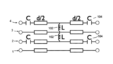
12. By loading the CPW and CSL modes with shunt inductors 102 and series
capacitors 104,
as shown in Fig. 2, these modes are forced to support only a negative-
refractive-index (NRI)
mode (also referred to as backward, or left-handed). The PPW and CPW modes can
be made
to couple strongly, and their contradirectional nature causes a substantial
bandgap to form.
Fig. 2 shows a unit cell 110 except that the capacitors 104 are shown twice
(at the top and
bottom); multiple unit cells can be arranged in series (and in parallel with
the addition of
more conductors).
[00127] In another embodiment the host TL selected is the shielded
conductor-backed
coplanar waveguide (S-CBCPW), which is shown in cross section in Fig. 4. Fig.
5 shows a
top view of the center layer of the S-CBCPW 106 or top layer of the CPCPW.
Since both the
series and shunt loading components can be inserted into the three coplanar-
waveguide
(CPW) conductors on the same plane (conductors 2, 3, and 4 in Fig. 4), this
host TL enables
a fully uniplanar design without the need for vias. Furthermore, the presence
of the
conductor backing (conductor 1) and shield (conductor 5) allow for the
interaction of the
19
CA 02936482 2016-07-19
CPW mode with parallel-plate waveguide (PPW) modes, supported between these
conductors and those of the CPW. The two parallel-plate modes, corresponding
to fields
above or below the CPW conductors in Fig. 4, will be referred to as the upper
and lower
PPW modes, respectively. When the upper PPW region is air-filled (cu= 1) and
its height hu
is sufficiently large (typically hu V10), it has been found that the upper PPW
mode can be
an effective low-frequency model for a loosely bound TA//0 surface-wave (SW)
mode.
[00128] As with the CPCPW embodiment, this MTL system not only supports the
PPW and CPW modes, but also a coupled slot-line (CSL) mode. Figs. 7-9 and 10-
12, which
depict the electric-field lines corresponding to these modes for the CPCPW,
also apply to the
modes for the S-CPCPW, with the addition of the upper PPW mode (not shown) for
the S-
CPCPW. These TEM modes may be classified as either even or odd, based on their
electric
field distributions. The even modes are described by an electric field tangent
to the symmetry
plane indicated by the white dashed lines in Figs. 10 through 12 (equivalent
to a perfect-
magnetic conduction (PMC) boundary), while the odd nodes can be considered to
be those
which support an electric field normal to the symmetry plane (equivalent to a
perfect-
electric-conducting (PEC) boundary). Even modes have the potential to couple
with other
even modes (and likewise for odd modes) while even and odd modes do not
couple.
According to these definitions, the PPW, CPW, and SW modes are even modes,
whereas the
CSL mode is odd.
[00129] MTL theory can be used to model this system. The host TL properties
are
determined by extracting the per-unit-length capaCitance and inductance from
finite-element-
method (FEM) simulations (assuming PMC boundaries on the transverse edges of
the S-
CBCPW TL, as indicated by the dashed lines in Fig. 4), from which propagation
constants
and characteristic impedances are derived. The TL-MTM unit cell is created by
periodically
loading the waveguide structure with series capacitors and shunt inductors, as
shown in the
MTL equivalent circuit in Fig. 6 for the S-CBCPW version or in Fig. 3 for the
CBCPW
version.
[00130] The dispersive properties of the TL-MTM can be analyzed by assuming
an
infinite cascade of unit cells. Firstly, the unit-cell equivalent circuit in
Fig. 3 or Fig. 6 is
CA 02936482 2016-07-19
generalized to an-ABCD transmission network, in which the input field
quantities (currents
and voltages) of the nth unit cell are related to those at the output as
follows:
rni 111 [B]l iFin+3.1 [[A] [B]1 VT1 e-yd
)
1161 [DM 171+ [C] [D]] in
[00131] Bloch's theorem has been invoked to relate the input and output
circuit
quantities between the ports as indicated, where d is the physical length of
the unit cell
imparted by the host TL and[A] is the sub-matrix of the unit cell's
transmission matrix
describing the transmission of voltage across the ports. The propagation
constants 7 ¨ a +j3
represent the complex coupled Bloch-mode solutions supported by this system.
Using (1)
and the commutative property of the sub-matrix components of the symmetric,
reciprocal
transmission network, the Bloch modes can be simply expressed as the solution
to the
characteristic equation,
detaA] ¨ [I] cosh(yd)) = 0 (2)
from which the frequency dispersion of each of the modes (y as a function of
w) may be
obtained. An example one-dimensional dispersion diagram, based on the
equivalent circuit in
Fig. 6, is shown in Figs. 13A and I3B, which respectively present the
dispersions of the
coupled and corresponding isolated modes. These diagrams will be used to
explain several
notable features. Since the odd (CSL) mode does not couple with the other
modes, its
dispersion curves have been omitted for clarity.
[00132] Referring to Figs. 13A and 13B, the dashed-dotted black line
represents the
vacuum light line, while the dotted line represents propagation in the
substrate dielectric, or
equivalently, the dispersion of the isolated PPW mode. The solid grey lines
correspond to I3d
= Im()d), while the dashed grey lines correspond to ad = Re(yd). Generally,
the sign of the
slope at any point of the 3d curves on this diagram indicates the direction of
the mode's
group velocity (hence, direction of power flow) relative to its phase
velocity. Since here we
excite the coupled system using a PPW mode, we establish the reference that
power flows
into the system in the forward direction. Therefore, for the purposes of the
present
discussion, a positive slope corresponds to a power flow in the positive
direction, and
likewise a negative slope indicates power flow in the negative direction.
21
CA 02936482 2016-07-19
[00133] It is worth noting that the attenuation constants shown in Fig. 13A
and 13B do
not correspond to resistive losses, which were not considered in the
analytical derivation of
these modes, but rather represent reactive attenuation due to two distinct
mechanisms. The
first mechanism arises from a mode being cul-off, which is to say that the
propagation
constant exhibits 13 a. This describes an evanescent mode, in which power is
reflected due
to an inability of the system to support propagation. The second mechanism
arises from
contradirectional forward-backward coupling. In this case, attenuation results
from the
coupling of power from one mode travelling in one direction into another mode
travelling in
the opposite direction, such that there is no net transmission of power for
the infinite periodic
structure. Since propagation occurs simultaneously with attenuation, the
coupled mode is a
complex mode exhibiting a complex propagation constant with a ;=,13. The
presence of either
form of attenuation may be exploited to suppress modes of interest.
[00134] To begin, it is worthwhile considering the dispersions of the
isolated (even)
modes, which are determined by removing the unnecessary conductors from the
MTL
equivalent-circuit model. The TL properties, however, are computed assuming
that these
conductors exist, but serve only as parasitic elements. The origin of these
modes is evident
from the unit cell in Pig. 2 (illustrated for the CPCPW but also applicable to
the S-CPCPW;
the conductor backing, present in both versions, and shield, present in the S-
CPCPW version
only, are both omitted)and its MTL equivalent-circuit model (for the S-CPCPW
version) in
Fig. 6. In particular, it can be seen that the shunt capacitors and series
inductors serve to load
the CPW mode, such that it exhibits a backward characteristic. The forward
characteristic of
the PPW modes are largely unaffected by the loading.
[00135] Coupling between these isolated modes has two criteria: 1) mode-
matching of
the transverse fields, and 2) phase-matching in the longitudinal direction.
The CPW and
PPW modes exhibit a large degree of field overlap, and this satisfies the
first criterion. The
second criterion is satisfied where the two isolated-mode dispersion curves
intersect on the
dispersion diagram.
[00136] Recognizing these features in the coupled system of Figs. 13A and
13B,
several regions may be identified. At low frequencies, only the PPW modes
propagate. As
frequency increases towards 2.4 GHz, the lower PPW mode becomes increasingly
dispersive
22
CA 02936482 2016-07-19
as it couples more strongly with the backward CPW mode. At 2.4 GHz, the CPW
mode
starts to propagate; however, since it is strongly coupled with the lower PPW
mode, the
contradirectional power flow between the forward lower PPW mode and the
reactively
loaded backward CPW mode results in a complex mode bandgap from 2.4 to 5.0
GHz. It
should be noted that the portion of the attenuation (ad) curve above 5.0 GHz
which exists
between 60 and 90 corresponds to the cutoff CPW mode, and is not part of a
complex-
mode system with the propagating lower PPW mode above 6 GHz. From 5.0 GHz to
6.0
GHz, the lower PPW and CPW modes start to decouple, after which propagation of
the
lower PPW mode begins to be restored (identified by the slope of the asymptote
at higher
frequencies). The CPW mode's propagation is not restored until well above 10
GHz. Lastly,
there is weak coupling between the forward lower PPW mode and forward upper
PPW mode
near 6.5 GHz. Although in this document we focus exclusively on the even
modes, it is
worth noting that the odd CSL mode has a bandgap between 6.5 and 7.0 GHz and
is cut off
below 3.2 GHz. It is unaffected by the coupled system, since being odd it does
not directly
couple with any other supported mode.
[00137] The theory presented above was validated using a proof-of-concept
design,
which possesses a one-dimensional layout for ease of design, fabrication, and
characterization. The EBG is designed for fabrication on a single substrate,
and as an initial
goal of the design, suppression of the (lower) parallel-plate mode is sought
between 2.4 and
6.0 GHz. A unit cell is designed with use of the equivalent-circuit model to
be electrically
small and to employ low-valued LC loading, which enables its realization in
fully printed
fashion. Theoretically, this topology can be modelled using the conditions
previously given
for the modelling of the SW mode ¨ that is, the upper dielectric may be
assigned a relative
permittivity of 1, and the shield height (hi,) may be made sufficiently large
(100 mm is used
in this case).
[00138] The *out of the LC-loaded CPW layer of the designed unit cell 110
is
shown in Fig. 14; the dimensions of the design are the unit cell period d = 5
mm, width w =
mm, the CPW strip line width s = 0.2 mm, the CPW gap width g = 0.5 mm, loading
capacitor length g, = 0.8 mm, and loading inductor width WI,¨ 0.2 mm. A
minimum feature
size of 0.2 mm is used for the interdigitated capacitor's finger and gap
widths, for ease of
23
CA 02936482 2016-07-19
fabrication using standard etching processes. The printed loading components
are designed
(estimated using empirical formulas and then mildly tuned in simulation) to
provide loading
values of C = 0.8 pF and L = 0.8 nH. The properties of the dielectric (hi =
1.524 mm, cr
3.66, tan 6' = 0.004, and 1-oz. copper cladding on both sides with a bulk
conductivity of
5.8x10⁷ S/m) are determined by the preselected substrate (RogersTM R04350Tm).
[00139] The EBG's dispersive properties were confirmed by performing an
eigenmode simulation in HFSS. This simulation setup involves embedding the
unit cell in a
vacuum box with a perfectly matched layer, master/slave, and PMC boundaries
applied to
the top surface, longitudinal faces, and transverse faces, respectively. These
support the
necessary fields to simulate an infinite array of unit cells in the transverse
direction.
[00140] The results of this simulation for the even-mode solutions are
shown in Fig.
15, along with the curves obtained from the MTL equivalent-circuit model. The
solid curves
dispersion data for the equivalent-circuit model of Fig. 6 and the large dots
show data
simulated using HFSSTM. Generally, they demonstrate excellent agreement, but
there is a
moderate divergence between these data towards larger fld values. This is
attributed to the
fact that the printed loading components cannot strictly be regarded as
lumped, as assumed
by the equivalent-circuit model; indeed, they are frequency-dependent, and
this attribute is
most evident when they are responsible for generating large phase shifts per
unit cell.
[00141] The weak interaction between modes near 6.5 GHz validates the
previous
statement that the vacuum-filled upper PPW mode with a relatively large height
(as was
modelled as described above) can be a good approximation for the loosely-bound
T Mo SW
mode, since an open boundary condition, rather than a shield conductor, was
used above the
EBG layer in this simulation. This is a behaviour which may be exploited in
the formation of
SW bandgaps, such as in the design of SW-suppressing ground planes for antenna
applications.
[00142] The parallel-plate-mode suppression ability of the EBG structure
was
examined by simulating the scattering parameters of the PPW mode. Using HFSS,
nine EBG
unit cells were cascaded and the (lower) PPW mode was excited using waveports.
PMC
boundary conditions were again used on the transverse faces, and a radiation
boundary was
used on the remaining faces above the unit cells. A 25 mm section of unloaded
PPW was
24
CA 02936482 2016-07-19
used to interface the waveports to the EBG. The results of this simulation are
shown by the
solid and dashed curves in Fig. 16. The solid curve shows simulated data for
the S11
scattering parameter, the dashed curve shows simulated data for the S21
scattering parameter,
the dotted curve shows measured data for the Si i scattering parameter, and
the dash-dotted
curve shows measured data for the S21 scattering parameter. The 10-dB
insertion-loss points
indicate a bandgap region from approximately 2.6 to 6.4 GHz, which is very
close to the
design criteria, and also very close to the dispersion data given by the HFSS
eigenmode
simulation. These results validate the accuracy and utility of the equivalent-
circuit approach
in predicting and designing the EBG bandgap properties.
[00143] To confirm the simulation results, a PCB containing the designed,
fully
printed EBG was fabricated. Using a 60-mil (i.e. 1.524-mm-thick) RogersTM
R04350TM
substrate, a 5 x 9 grid of unit cells was connected to a PPW, in order to
sufficiently
approximate the simulation setup. This PPW was then linearly tapered to a 502
microstrip
(MS) line for ease of measurement. The fabricated structure is shown in Fig.
17, along with
the appropriate dimensions. The total length of the EBG is 45 mm, and the
total width is 50
mm. The length of the PPW region on either side of the EBG is 10 mm, and the
microstrip
sections are 20 mm long and 3.3 mm wide. The linear tapers connecting the PPW
and MS
were 50 mm long. SMA connectors were used to interface an AgilentTM
Technologies
N5244A vector network analyzer (VNA) with the PCB to perform the measurements.
[00144] The measured data are plotted in Fig. 16 along with the simulated
data, and it
is clear that they exhibit very good general agreement, despite the finite
width of the EBG
section and the large taper and microstrip sections, which were not included
in the simulation
model. Indeed, in both data the bandgap behavior of the EBG is clearly visible
between 2.6
GHz and 6.4 GHz, as indicated by the dashed vertical lines. It should be noted
that the
resonant behavior below the bandgap region is owed to Fabry-Perot resonances
of the highly
dispersive coupled PPW-CPW mode. Discrepancies in the upper pass band may be
attributed
to the frequency response of the microstrip and taper sections in the
fabricated device.
[00145] It is worth noting that the electrical size of the unit cell over
the designed
bandgap region ranges from approximately Ig/12 to Ig/5, wherelg is the
wavelength in the
dielectric. This demonstrates the strong degrees of miniaturization possible
with the TL-
CA 02936482 2016-07-19
MTM approach, which can be further appreciated by noting that the strength of
the loading
components (and hence miniaturization) is only limited by the minimum feature
size of the
manufacturing process.
[00146] TWO-DIMENSIONAL RADIAL EBG
[00147] The validation of the bandgap properties of the ID EBG prompts us
to
examine whether it may be straightforwardly extended to parallel-plate mode
suppression in
multilayer, 2D applications. For example, parallel-plate noise is detrimental
to signal
integrity in high-speed PCBs, which contain multiple ground and/or power
layers. This noise
can be created by the routing of signal paths between layers with the use of
vias, and the
resulting noise propagates away radially through parallel-plate modes. In
order to suppress
this noise, a 2D solution is required. An EBG is provided here which can be
constructed in
radial form to decrease coupling between two parallel vias, as shown in Figs.
18 (top view)
and 19 (side view). Plural electromagnetic structures as described above are
arranged
arranged in parallel to surround a central area. This EBG, generally indicated
by reference
numeral 112, is composed of trapezoidal sections 114, which are slightly
distorted sections
of cascaded one-dimensional unit cells that have been arranged side-by-side in
order to form
a complete circle. Note that in this embodiment the widths of the inductors
102 have been
dramatically increased, and the lengths greatly shortened, in comparison to
embodiments
discussed above.
[00148] This setup is similar to that used in R. Abhari and G. V.
Eleftheriades,
"Metallo-dielectric electromagnetic bandgap structures for suppression and
isolation of the
parallel-plate noise in high-speed circuits," IEEE Trans. Microw. Theory
Tech., vol. 51, no.
6, pp. 1629-1639, 2003, which compared the transmission between two vias in a
bi-layer
medium with and without a Sievenpiper mushroom EBG, in order to determine its
effects.
The Sievenpiper structure operates extremely well as an EBG, but its
construction is
complicated by the requirement for a via for each unit cell. The proposed
radial EBG enables
the suppression of signals coupled into the parallel-plate mode through 2D
cylindrical waves,
while maintaining its simplistic 1D, uniplanar design approach. To demonstrate
the
versatility of the design procedure and exploit its fully printed nature, this
EBG is designed
26
CA 02936482 2016-07-19
. ,
to present a bandgap around X-band, where discrete (surface-mount) inductors
and
capacitors cannot be used due to their typically low self-resonance
frequencies.
[00149] This embodiment of an EBG is designed to suppress the upper
parallel-plate
mode supported by a hi, = 0.254-mm (10-mil) RO3OI0TM = 10.2, tan 6 =
0.0035)
substrate. The EBG is realized on the bottom metallization layer and the unit
cell has the
following properties, in keeping with the symbols previously introduced: d =
2.5 mm, w =
1.6 mm (average), s = 0.1 mm, g = 0.1 mm, wi, = 0.7 mm, g, = 0.7 mm, with the
interdigitations each 0.1 mm wide and spaced 0.1 mm apart. The EBG is
interfaced with a hi
= 1.524-mm (60-mil) FR-4 (Ei = 4.2, tan 6 = 0.0016) layer placed below the
R03010Tm
layer, which serves as a low-cost shielded substrate.
[00150] The EBG comprises three unit cells in the radial direction, and in
its full
radial form, employs 36 unit cells around the azimuth. The vias, which are
used for both
excitation and detection, and which were designed to be connected to 50-Q,
teflon-filled
SMA connectors, are separated by 20 mm. The distance between the center of the
excitation
via and the inner radius of the EBG is 7.5 mm. It should be noted that the
theory disclosed
above allows these dimensions to be considerably reduced if necessary through
various
design choices such as using a smaller number of unit cells (at the expense of
suppression
ability), or using an etching process that could produce reduced feature
sizes, which would
allow for increased loading component values and hence a smaller period and/or
increased
bandgap width. These techniques would prove advantageous where space is
limited, e.g., in
systems with densely packed vias.
[00151] B. Simulation - Absorbing Boundaries
[00152] The case of an effectively unbounded PPW medium was investigated
first in
order to establish the 'realistic suppression ability of the EBG unobscured by
multiple
reflections that would be introduced by finiteness of the simulation domain.
This was
accomplished by placing absorbing boundaries around the edges of the finite
PPW medium
in simulation. The transmission response of this EBG, as measured through the
upper layer
RO3OIOTM dielectric, was simulated over a single radial section (as indicated
in Fig. 18) with
PMC transverse boundary conditions. The resulting scattering parameters are
shown in Fig.
20, which reveal a suppression of around 20 dB over the 7.5 mm extent of the
EBG.
27
CA 02936482 2016-07-19
[00153] The resulting scattering parameters of the complete EBG are shown
in Figs.
21 and 22. Suppression across the X-band by up to 50 dB is observed when the
EBG is
present. Resonant interactions caused by coupling between the vias and the 2D
EBG
structure are observed at some frequencies (e.g., at 7.0 and 11.3 GHz). These
resonant
frequency points were investigated and found to depend on a number of factors,
such as the
radius of the exciting vias, the inner radius of the EBG, and the number of
EBG unit cells
employed radially ¨ as such, they could likely be mitigated through a number
of design
choices which vary some or all of these parameters. Nevertheless, even with
these
resonances, the suppression maintains significant improvement over the case
without the
EBG at all frequencies.
[00154] Figures 23 and 24 examine the simulated fields respectively at 9
GHz (the
frequency exhibiting maximum parallel-plate-mode suppression) and 5 GHz
(outside the
EBG bandgap). They detail the complex current-density magnitudes (plotted on
an identical,
logarithmic scale) on'the metallization layer at the boundary between the
RO3OIOTM and FR-
4 dielectrics, which contains the EBG (the same layer shown in Fig. 9a). The
excitation via is
on the left-hand side surrounded by the EBG. At 9 GHz, the EBG effects a drop
in the field
level by approximately two orders of magnitude (40 dB), confirming the
suppression
suggested by the scattering parameters. The null between the EBG and the
excitation via is
evidence of the standing wave created by the signal being reflected by the
EBG, and is
noticeably absent at 5. GHz, where the EBG essentially completely transmits
the (upper)
PPW mode. From the corresponding cross-sectional complex magnitudes of the
electric
fields (calculated but not shown here) it can be seen that the field decay
primarily takes place
inside the EBG region as expected. There is some field leakage into the FR-4
layer, but it
appears to be confined within the EBG region and is relatively small in
magnitude
(approximately 10 dB lower than the maximum fields in the RO3O1OTM
dielectric). At 5
GHz, the fields are still constrained by the EBG (the currents must still pass
through the thin
CPW strips), but there is much less suppression as indicated by the field
strengths over the
outer-most unit cells. There is also slightly less leakage into the lower
dielectric, indicating
that the PPW mode in the upper dielectric is better guided by the EBG at this
frequency.
[00155] Simulation - Open Boundaries
28
CA 02936482 2016-07-19
[00156] To enable comparison to a fabricated prototype, which would possess
finite
dimensions, the EBG was also simulated with open boundaries, with both layers
of size 60
mm x 80 mm and embedded in vacuum. Figures 25 and 26 show the resulting
simulated
scattering parameters, for which up to approximately 40 dB of suppression and
a
corresponding improvement in return loss is observed over the frequency range
of 7.5-11.5
GHz, corresponding to up to roughly 67 dB per guided wavelength of
suppression. This is
slightly lower, but comparable with reported results for Sievenpiper EBGs,
which have had
suppression of up to roughly 75 dB per guided wavelength for a similar two-
layer setup, or
roughly 95 dB per guided wavelength for a UC-EBG. Other suppression mechanisms
such as
high-dielectric-constant rodded photonic crystals have reported up to roughly
92 dB per
guided wavelength, and circular high-impedance surfaces have been reported to
obtain up to
roughly 100 dB per guided wavelength. However, it should be recalled that our
proposed
unit cell is uniplanar, and therefore much easier to fabricate, as well as
having a bandgap that
may be accurately designed using MTL theory, both of which provide clear
advantages over
these other devices. The apparent noise in the resulting data is due to the
fact that the open
boundaries of the finite-sized PPW (which is electrically large at X-band)
create reflections
that establish a large number of 2D resonances (cavity modes).
[00157] D. Experiment
[00158] The PPW with EBG was fabricated by LPKF Laser & Electronics AGTM
using a high-resolution laser-based PCB prototyping system, and is depicted in
Fig. 27. The
vias were realized with the use of flush-mount SMA connectors attached the the
top face of
the upper conductor, for which the center pin was clipped and soldered to the
back side of
the middle conductor:
[00159] The two layers (FR-4 and RO3OIOTM) were compressed together using
two
clamps. The pressure was distributed with the use of a hard plastic spacer
with a rectangular
aperture (approximately 25 mm thick) and a layer of firm styrofoam
(approximately 14 mm
thick). A layer of masking tape was used to hold the two dielectrics together
and prevent
them from sliding laterally.
[00160] The measured results are indicated in Fig. 28 and 29. These data
exhibit a
frequency up-shift relative to the simulated case, which could be attributed
to a slightly
29
CA 02936482 2016-07-19
=
lower cu resulting from substrate tolerances and possibly from a small air gap
between layers
(since the layers were not bonded by any means, but rather manually compressed
together
during measurement). It was found that if the simulation was re-run assuming
an average
dielectric constant of c11= 9.7 and an average air gap of 50um between layers,
then the
simulated and measured data sets matched reasonably well, as shown in the
figures.
[00161] The proposed EBG could prove useful in mitigating the effects of
PPW-mode
excitation in several applications noted at the beginning of this work,
including coupling
reduction between adjacent substrate integrated waveguide (S 1W) circuits,
reduction of
parasitic PPW coupling in conductor-backed aperture-coupled patch antennas,
and even the
design of miniaturized and/or multi band patch antennas as disclosed below. SW
applications
of the EBG are suggested by the observed coupling between the T Alo surface-
wave mode
and the even modes of the S-CBCPW structure. This coupling may be exploited in
many
applications, including the mitigation of multipath interference in global
navigation satellite
system (GNSS) antennas, affording additional degrees of freedom in steering
surface waves
on surface-wave antennas and launchers, and generally in miniaturizing surface-
wave
components. Incidentally, the odd CSL mode could be used to couple with T E
surface-wave
modes, creating odd-mode bandgaps. Furthermore, the coupling between the even
modes
(odd modes) and the T (T E) surface-wave modes results in dispersion features
inside the
light line, which Could be used in combination towards the design of
miniaturized dual-
polarized or circularly polarized leaky-wave antennas.
[00162] Thus, a uniplanar EBG and MTL equivalent-circuit model have been
proposed for the suppression of parallel-plate modes. This EBG is based on the
TL-MTM
and operates on the principle of contradirectional coupling between the one of
the forward
PPW modes and the backward CPW mode of a S-CBCPW structure, providing a large,
controllable stopband. This allows for a uniplanar, printable design without
any vias or
discrete (surface-mount) elements, which makes it both low-cost and suitable
for high-
frequency applications. The dispersion of the supported modes was verified by
full-wave
simulation, and the transmission properties of the PPW mode were confirmed by
simulation
and in experiment. All of these results demonstrated very good agreement,
validating the
accuracy of the MTL equivalent-circuit model. The suppression of radially
propagating
=
CA 02936482 2016-07-19
=
PPW-mode noise in multilayer PCBs between vias was suggested as a practical
application
and also validated in simulation and experiment. The ID EBG was radially
arranged around
a via, and this was found to suppress the radially propagating PPW mode in two
dimensions
by approximately 50 dB at X-band over a length of just 7.5 mm.
[00163] A PRINTED DUAL-BAND ELECTROMAGNETIC BANDGAP
STRUCTURE GROUND PLANE FOR GNSS ANTENNAS
[00164] There is provided a novel ground plane design for GNSS antennas.
The
ground plane is a printed circuit board which contains electromagnetic bandgap
structures
which suppress the effects of multi path interference at two independent
frequencies. This is
accomplished by the suppression of surface waves which travel on such
conductive ground
planes, the end result of which is decreased left-handed circularly polarized
receiver
sensitivity above and near the horizon.
[00165] The novel structure introduced here is an EBG which operates at two
distinct
frequencies and is completely uniplanar without discrete (i.e., surface-mount)
loading
components, such that it can be fully printed using standard printed circuit
board (PCB)
manufacturing techniques. Furthermore, the design of this EBG is based on the
transmission-
line (TL) metamaterial, which can enable strong miniaturization of the EBG
unit cells.
[00166] The developed EBG is based on the popular PCB waveguide, conductor-
backed CPW (CBCPW), as shown in cross section in Fig. I, or in top view in
Fig. 5.
Referring to Fig. 5, propagation is in the x-direction. As discussed above, it
consists of four
independent conductors, and therefore supports three quasi-TEM modes, as shown
in Figs. 7
through 9, and with a three-dimensional view of the waveguide in Figs. 10
through 12. These
modes are the parallel-plate waveguide (PPW) mode, the coplanar waveguide
(CPW) mode,
and the coupled slotline (CSL) mode. This structure also supports a SW mode on
the three
upper conductors. Fig. 5 details the properties of the upper conductor layer.
The unit cell
length is d, the CPW strip width is s, and the CPW gap with is g. The
dielectric height (not
labelled) will be referred to as h.
[00167] The bandgap properties of the EBG are obtained by loading this
waveguide
(referred to as the "host"), with capacitors and inductors.
3 I
=
CA 02936482 2016-07-19
[00168] Bandgaps are formed by creating the conditions under which modes
exchange
power. Metamaterial modes have the capacity to carry power in the opposite
direction of
their propagation, suCh that all of the power entering a metamaterial region
can be guided in
any desired direction, including the direction from which it arrived
(reflection). The
proposed EBG design exploits modal coupling to reflect surface waves, as well
as couple
them into the dielectric, in order to prevent them from reaching the antenna
element. By
coupling the PPW mode with the loaded CPW mode, a new dual-band mode is formed
which in turn couples to the SW mode to form SW bandgaps. Importantly, both of
these
modes (PPW and CPW) are required to exist in order to create the dual-band
functionality of
this EBG, and therefore each of the four conductors is necessary for this dual-
band design.
[00169] In the embodiment described here, a layout is used that has the
features of the
layout shown in Fig 2, but instead of a continuous center conductor of the
upper conductor
layer, center capacitors 116 are introduced to that conductor in parallel with
the capacitors of
the side conductors of the upper conductor layer. The capacitors are inserted
into slots where
the conductor has been removed from the CPW strip line (center conductor) and
grounds
(side conductors), whereas the inductors are inserted into the CPW gaps. These
loading
components can be realized in a manner compatible with a PCB process. An
equivalent-
circuit model of this loaded structure (for propagation along the x-direction)
is shown in Fig.
31. The value L is the equivalent shunt loading inductance, the value Cs is
the equivalent
series loading capacitance in the CPW strip line, and the value C, is the
equivalent series
loading capacitance in each of the two CPW grounds.
[00170] This equivalent-circuit model can be analyzed using a periodic
analysis to
yield the EBG's dispersive properties (phase shift across the length d as a
function of
frequency), from which the bandgaps in the SW mode can be readily observed.
Fig. 32shows
such a numerically computed dispersion diagram, for which the SW mode on a
solid
conductor is represented by the solid back line. The dots represent points
solved in the
numerical simulator for the EBG structure, for which it can be seen that two
"gaps" exists in
which the black line does not overlap the dots. The gaps are the SW bandgaps
created by this
structure, and are a critical feature of the EBGs behaviour. The other regions
that were found
in the numerical simulator (indicated by the black dots) represent the
coupling of the CPW
32
CA 02936482 2016-07-19
=
and PPW modes, which as previous stated are necessary for the formation of the
SW
bandgaps.
[00171] A prototype ground plane was designed for operation at GPS LI and
L2,
using a RO3OIOTM dielectric (relative permittivity Cr = 10.2) with a thickness
of 50 mils (1.27
mm). Referencing Fig. 5, the constituent unit cells were designed to have a
length d = 29mm,
width w = 20mm, CPW strip widths = 2.5mm, and CPW gap widths g = 2mm. The
loading
components L, Cs, and Cg are realized by strip inductors and interdigitated
capacitors, both
of which can be created in a standard PCB etching process, as shown in Fig.
33.The bandgap
frequencies can be adjusted at this stage by tuning Cs and Cg. The dimensions
of features of
the interdigitated capacitors are labelled in Figs. 34 and 35. The CPW strip
line capacitor has
Ns = 7 fingers, length Ise = 4.7mm, finger spacing gfs = 0.2mm, and finger
width Wfs =
0.2mm. The CPW ground capacitors have properties Ng = 9 fingers, length lg, =
0.6mm,
finger spacing gfg = 0.2mm, and finger width wfg = 0.2mm. The strip inductors
have a width
of wi =1.0 mm.
[00172] Once this design is complete, three of these unit cells are
cascaded, and
distorted into a trapezoidal arrangement 118 by removing sections of the
dielectric around
the outer edges of the CPW grounds, as shown in Fig. 36. The trapezoid has an
arc length of
12 , and an average width wa = 20mm.
[00173] These trapezoidal sections can then be cascaded side-by-side into a
closed
circle 120, as shown in Fig. 37 (The four holes have been drilled through this
dielectric to
host coaxial feed lines for the antenna element (not shown)). The arc length
of the
trapezoidal sections determine how many unit cells can be arranged azimuthally
to form a
circle, and should therefore be an even factor of 360 (e.g., 12 degrees). The
width of the
first unit cell will then determine how large the diameter of the resulting
circle will be - in
this design, the inner diameter c = 100mm and the outer diameter e = 274mm.
The inside of
the ground plane is a solid conductive layer. This final ground plane can be
manufactured in
its entirety using a standard PCB process on a single layer dielectric. The
back side of the
dielectric is simply a solid conductor.
[00174] This design was simulated along with a stacked patch antenna at
these
frequencies. It was compared with the original antenna element without an
extended ground
33
=
CA 02936482 2016-07-19
plane, and an extended solid conductive ("bare") ground plane with the same
radius as the
EBG ground plane. The simulation results indicated that the LHCP is
significantly
suppressed on and above the horizon at both Li and L2. The axial ratio (AR) is
low and the
multipath ratio (MPR- the ratio of RHCP at a point to the LHCP on the opposite
side of the
horizon) is increased near the horizon, as desired.
[00175] Dual-band Microstrip Patch Antenna Using Integrated Uniplanar
Metamaterial-Based EBGs
[00176] There is provided a novel dual-band microstrip patch antenna that
employs a
metamaterial-based EBG (MTM-EBG) integrated into its radiating edges to create
two
distinct operating frequencies. The resulting antenna is compact, uniplanar,
completely
printable, and via-free. Dispersion engineering of the MTM-EBG unit cell
through a rigorous
MTL analysis allows easy design for two or more arbitrary frequencies.
Additionally, a
novel approach is taken to employ the same MTM-EBG to impedance-match the
antenna to
an inset microstrip feed at both operating frequencies. A dual-band MTM-EBG
antenna
designed to radiate at 2.4 GHz and 5.0 GHz is simulated and tested, and
experimental results
demonstrate radiation performance comparable to the corresponding conventional
patch
antennas in excellent agreement with simulations, while also affording some
degree of
miniaturization at lower frequencies.
[00177] Many approaches have been taken to yield dual- or multi-frequency
operation
of microstrip patch antennas, which may be expensive and/or difficult to
implement. Early
efforts introduced "stacked" patches, in which patches of different sizes are
layered
vertically with each underlying layer serving as the effective ground plane of
the above
patch, which may be directly or parasitically excited. A more simple
arrangement involved
parasitically exciting patches on the same layer allowing for a single-layer
design; however,
the parasitic coupling was found to be much less effective in this
orientation. Exciting
various cavity modes on asymmetric patches has been used; however, this
technique
inherently requires that the excited modes have different field profiles,
polarizations, and
possibly different feeding mechanisms, which may not always be desired. A
popular current
method of exciting various modes in a fully planar structure employs slots
etched into the
patch or ground plane, but such approaches tend to be empirical and are,
therefore, ill-
34
CA 02936482 2016-07-19
equipped for systematic design. Some designs may employ loading with non-
planar
components such as vias, but these add to manufacturing complexity. Other
antennas,
particularly those employing frequency-dependent dispersive properties,
achieve multi-band
operation through the excitation of a number of different resonance
mechanisms; however,
these behaviours tend to come at the expense of gain and polarization purity.
Moreover, the
radiation patterns of these antennas do not typically resemble those of the
fundamental patch
mode for all radiating frequencies.
[00178] More recently, metamaterial (MTM) structures have been integrated
into the
design to produce multiple resonances. MTMs are artificial structures
possessing properties
that may transcend those typically found in nature.
[00179] A class of these materials known as transmission-line (TL) MTMs are
particularly useful in engineering dispersion properties in TL environments
such as
microstrip or parallel-plate waveguide (PPW), created by appropriately loading
a TL with
discrete inductors and capacitors at deeply subwavelength intervals. Moreover,
the
dispersive properties of these structures can typically be accurately modelled
with an
equivalent circuit employing TL theory.
[00180] While.the MTMs used in many of these works pose fabrication
difficulties,
such as the use of large numbers of vias, embodiments of TL MTMs disclosed in
this
document avoid these complications. For example, the ID uniplanar
electromagnetic
bandgap (EBG) structure illustrated in Fig. 2, and with equivalent circuits
CBCPW and S-
CBCPW versions shown in Figs. 3 and 6 respectively, introduced and
characterized for the
suppression of PPW modes is ideal for PCB integration. This MTM-inspired EBG
(or MTM-
EBG for short) consists of electrically small unit cells and employs the
contra-directional
coupling between a PPW-like mode and a left-handed co-planar waveguide (CPW)
mode to
create a large bandgap that can be accurately described with multiconductor TL
(MTL)
theory. Therefore, the dispersive and bandgap properties of this material can
be controlled
and altered in a predictable manner, making it a suitable candidate for a wide
range of
microstrip and patch-antenna applications.
[00181] Here, the MTM-EBG is integrated directly into the metallization
layer of a
microstrip patch antenna 122, as shown in Fig. 38. It is demonstrated that the
MTM-EBG
CA 02936482 2016-07-19
may be dispersion-engineered to present either bandgap or passband
characteristics, which
effectively modifies the electrical length of the patch as a function of
frequency. This enables
the patch's fundamental cavity mode to be excited at multiple different
frequencies, such that
all resonances possess the same polarization and radiation profiles. We
present a MTM-EBG
that enables dual-band operation of the patch by creating two different
resonant patch
lengths: one at a higher frequency, where the EBG operates in its bandgap so
the fields are
confined to the patch region, and another at a lower frequency where the EBG
allows PPW
propagation, and thus the patch operates as if it were electrically much
longer. In addition,
the antenna achieves miniaturization at the lower frequency due to the highly
dispersive
nature of the EBG's PPW mode. By implementing printable inductive strips and
capacitive
gaps into the MTM-EBG instead of using discrete (e.g., surface-mount)
components, the full
dual-band antenna can be printed in the patch metallization layer over a
uniform ground
plane, without the need for vias. Finally, owing to its accurate equivalent-
circuit MTL
model, the MTM-EBG can be carefully integrated to serve a second novel
purpose: to
provide a high degree of impedance matching at both of the antenna's
resonances.
Specifically, by adding a section of the MTM-EBG to the feed side of the
antenna, the
electrical length of the inset also changes with frequency. This approach
ensures that both
operating frequencies are well matched and produce gains comparable to those
of a
conventional patch antenna.
[00182] The proposed patch antenna makes use of the standard cavity model
by
replacing the perfect-magnetic-conductor (PMC) boundary conditions on the
radiating edges
with a frequency-dependent boundary condition realized by the MTM-EBG.
Specifically, the
MTM-EBG allows the TMio mode to be supported both at what will be referred to
as the
lower frequency (located in its dispersive, low-frequency propagating band)
and higher
frequency (located in its higher-frequency bandgap), with the lower frequency
being deter-
mined by a combination of the length of the cavity and the dispersive nature
of the MTM-
EBG, and the higher frequency being determined by the size of the cavity
without the EBG.
This method allows for the antenna to operate at two bands, which both
maintain a simple
excitation using a microstrip feed and the familiar radiative properties of
the TMIO mode.
36
CA 02936482 2016-07-19
[00183] In order to effect the frequency-dependent behaviour described
previously, a
specific type of EBG is required. Firstly, it must be capable of interacting
with the PPW
mode, which shares the transverse field profile of the TMio patch mode.
[00184] Secondly, its properties must be well known, since its response
must be finely
tuned in order to achieve the correct operating frequencies. Thirdly, the EBG
should be
uniplanar and via-less, as a simple antenna fabrication method is desired.
[00185] An EBG as disclosed above is such an EBG, and an MTL analysis was
developed and shown to accurately describe its dispersion features. The host
TL of the
MTM-EBG is a conductor-backed co-planar waveguide (CB-CPW), which supports the
interaction of a PPW-like mode and a CPW mode, of which the latter is made to
be left-
handed (i.e., it supports backward-wave propagation) using left-handed MTM
loading (series
capacitors and shunt inductors, as shown in Fig. 39). The contra-directional
coupling of these
two modes results in a bandgap consisting of both complex-mode and evanescent
frequency
regions. Geometric features and loading values of the unit cell determine the
position and
size of the bandgap. A typical dispersion diagram is shown in Fig. 40, in
which only the
coupled system of even-polarized modes (PPW, CPW, and TM0 surface-wave) is
presented
for clarity. Although other odd-polarized modes exist (e.g. coupled slotline),
these shall be
suppressed through the selection of a symmetrically placed feed. The bandgap
region
(shaded) describes complex and evanescent modes resulting from backward
coupling, where
propagation is strongly reactively attenuated.
[00186] The higher-frequency patch resonance is created by employing the
EBG's
PPW bandgap (from approximately 3.0 GILlz to 5.5 G1-1z in Fig. 40), for which
the PPW
mode is prevented from propagating and the fields are strongly and reactively
attenuated
inside the EBG. For the lower-frequency resonance, the EBG's highly dispersive
PPW mode
is employed (below 3.0 GI-lz in Fig. 40). At these frequencies, the PPW mode
still
propagates, but incurs large phase shifts with distance travelled. Since the
phase constant as
a function of frequency is known, the resonant frequency is determined by
noting that the
dispersion angle of the EBG plus the phase incurred through the unloaded
cavity must equal
180 degrees.
37
=
CA 02936482 2016-07-19
[00187] A unit cell was designed to realize the dispersion profile shown in
Fig. 40, in
which it can be seen that there is excellent agreement between the MTL theory
and full-wave
eigenmode simulations using Ansys HFSS. The substrate chosen for the unit cell
was Rogers
RO3003TM (c,- = 3.00, tan 6 = 0.0010, 1.524 mm thick and clad with 17 gm
copper on both
sides) as it exhibits low-loss properties and is a common inexpensive
substrate material used
in microstrip and patch-antenna applications. The effective loading values of
the unit cell are
L = 1.00 nH and C = 1.08 pF as defined in Fig. 39, with dimensions listed in
Table I. Note
that L and C are defined differently in Fig. 39 in relation to this discussion
of a patch antenna
as compared to Fig. 2. Whereas the dispersion diagram assumes an infinite
array of MTM-
EBG unit cells, the MTM-EBG employed in the patch antenna will necessarily be
limited to
a small, finite number of unit cells. Fig. 42 compares the return and
insertion losses through
both a single cell and'a cascade of three cells and confirms that even a
single cell is capable
of producing a bandgap, although it may be widened by using a larger number of
cells. In
fact, the bandgap edge frequencies are observed to approach the analytical
prediction as the
number of cells is further increased. To maximize compactness, the example
antenna
disclosed here employs a one-cell-long MTM-EBG, though in other embodiments
more cells
could be used. The bandgap region is more well-defined for the three-cell case
but strong
passband and bandgap regions are maintained for a single cell. Note that the
band edges
approach those predicted in the dispersion diagram (Fig. 40, shaded region in
both figures)
as the number of cells increases.
[00188] Lumped components are expensive, they complicate the fabrication
procedure, and their maximum operating frequencies are constrained by their
self-resonance
frequencies (typically several GHz). To mitigate these drawbacks, the MTM-EBG
cells can
be designed for minimal reactive loading to enable the use of fully printed
lumped elements,
which allows for a unit cell that is completely printable as shown in Fig. 41,
with dimensions
provided in Table II. Propagation is in the x-direction. The inductance of the
strip inductors
can be estimated using empirical formulas found in J. K. A. Everard and K. K.
M. Cheng,
"High performance direct coupled bandpass filters on coplanar waveguide," IEEE
Trans.
Microw. Theory Tech., vol. 41, no. 9, pp. 1568-1573, 1993, and the design of
interdigitated
capacitors can be guided by G. D. Alley, -Interdigital capacitors and their
application to
38
CA 02936482 2016-07-19
=
lumped-element microwave integrated circuits," IEEE Trans. Microw. Theory
Tech., vol. 18,
no. 12, pp. 1028-1033, 1970. Thereafter parametric tuning is used to achieve
the desired
values. Additionally, the resonant frequency of the resulting antenna provides
enough
information to determine the effective values of the inductive and capacitive
loading.
[00189] With an understanding of the properties of the MTM-EBG, the
operation of a
dual-band antenna can be considered. By applying a MTM-EBG to its radiating
edges, a
patch antenna is designed to operate at frequencies of 2.4 GHz (the "lower
frequency") and
5.0 GHz (the "higher frequency"). As a basis for comparison, corresponding
conventional
higher-frequency and lower-frequency patch antennas were designed with
identical
parameters lp, wp, and ip (Fig. 38) chosen to achieve resonance at the above
frequencies. The
inset length ip is important for impedance matching, as determined by the
design equations in
C. A. Balanis, Antenna Theory: Analysis and Design. Hoboken, New Jersey, USA:
John
Wiley & Sons, Inc., 2005. Note that, while the patch width was chosen to be
the optimal
width of the high-frequency antenna, the wider low-frequency patch width could
have been
chosen as well. Whereas this is an equally valid approach, it results in a
high-frequency
antenna that is much wider than it is long, and as a result, higher-order
transverse modes may
be excited. This leads to high levels of cross-polarization. Other patch
widths may also be
used. Fig. 46 shows an example antenna with a wider patch width than shown in
Fig. 38,
optimized for the lower frequency. Either width works sufficiently well, and
other widths
could also be used.
[00190]
Cony. Low-Freq. Cony. High-Freq. MTM-EBG
lp 35.15 16.67 16.80
wp 43.32 21.21 21.00
ip 10.40 4.80 4.50
wi 2.00 2.00 1.62
Wf 3.76 3.76 3.76
39
=
CA 02936482 2016-07-19
[00191] TABLE 1: Antenna design values in mm for the conventional patch
antennas
and the MTM-EBG antenna. Refer to Fig. 38 for parameter descriptions.
[00192]
MTM-EBG, Front side MTM-EBG, Feed side
lc = 5.90 5.50
wc 7.00 7.00
0.20 0.20
gL 0.80 0.80
gc 1.70 1.60
[00193] TABLE II: Design values for the MTM-EBG antenna's two MTM-EBG
regions in mm. Refer to Fig. 41 for parameter descriptions.
[00194] In general, inset length decreases when matching antennas at higher
frequencies, and this observation suggests a novel application for the MTM-
EBG: to
integrate it into the feed side of the antenna for a high degree of impedance
matching at both
operating frequencies. The difference in inset length can be expressed as an
electrical length,
and then a MTM-EBG cell can be designed from its dispersion diagram to have
this
electrical length at the lower frequency, while still reflecting at the higher
frequency. The
effect of this is that the inset length is frequency-dependent, and is
optimized for each
resonance.
[00195] The remaining electrical length needed for a resonance at the lower
frequency
can be easily calculated, and another EBG cell with appropriate dispersion
characteristics is
affixed on the front end of the patch. The MTM-EBG antenna should now resemble
each
individual patch at its respective operating frequency, and after simulation
only minimal
tuning (generally in patch length or MTM-EBG unit-cell length) should be
needed to ensure
the operating bands are at the desired frequencies.
[00196] The result of this process, as described below, is a well-matched
antenna that
operates in a standard patch TMio mode for both frequencies. Additionally, due
to the highly
dispersive nature of the MTM-EBG, the patch is moderately miniaturized at the
lower
CA 02936482 2016-07-19
frequency, with respect to the conventional low-frequency patch. The uniplanar
MTM-EBG
is shown to be ideal for this application, and the result is a practical,
fully printed, and
analytically designable dual-band microstrip patch antenna.
[00197] Following the design procedure given above, the dual-band MTM-EBG
antenna as well as conventional lower- and higher-frequency patch antennas
were simulated
and fabricated on a Rogers RO3003TM substrate. Dimensions of the antennas are
given in
Tables 1 and II.
[00198] Looking first at return loss shown in Figs. 43A-43D, it is evident
that the
MTM-EBG antenna is well matched, exhibiting a return loss better than 10 dB in
all cases.
The operating frequency is shifted up for the higher-frequency resonance by
about 3%,
though a 1% shift was also seen in the corresponding conventional antenna.
This may be
attributed to fabrication tolerances in the construction of the antenna
features, which are
particularly sensitive at higher frequencies. A final note on the return loss
is that the low-
frequency resonance of the MTM-EBG antenna is slightly more narrowband than
that of the
corresponding conventional patch; this is to be expected since, due to the
dispersive
properties of the MTM in its low-frequency transmitting region, a small change
in frequency
results in a correspondingly large change in electrical length.
[00199] Simulation provides further validation of the design concept by
producing
plots of the complex magnitude of the electric fields in the patch at the
operating frequencies
of the antennas. The simulated fields were plotted through the center of the
dielectric, and it
was found that the MTM-EBG regions behave precisely as desired, since for the
low-
frequency resonance they are clearly transmitting, yet for the high-frequency
case the fields
are confined to the patch region. In addition, each resonance strongly excites
the
fundamental TMio patch mode which implies that the radiation patterns of
corresponding
frequencies should resemble each other fairly closely.
[00200] The gains of the simulated antennas are compared in Fig. 44A-D.
Viewing the
MTM-EBG antenna in direct comparison with conventional patch antennas at the
same
frequency, it is apparent that the radiation patterns are very similar in
terms of both co- and
cross-polarizations. While the gain of the MTM-EBG patch antenna is almost
identical to
that of the conventional patch at the higher frequency, it is approximately
2.5 dB lower than
41
CA 02936482 2016-07-19
conventional patch at the lower frequency. While the MTM-EBG patch antenna
still remains
an effective radiator at this frequency, the degradation in performance is
likely due to small
scattering losses in the fine features of the MTM-EBG and to the decrease in
electrical size
of the antenna.
[00201] The directivities of both the conventional and MTM-EBG patch
antennas
were measured in an anechoic chamber for comparison to the simulation results.
Antenna
measurements initially showed high cross-polarization and a combination of
simulations and
rigorous measurements suggested that this was due to radiation from unbalanced
currents
along the coaxial feedline. A solution to this for the lower-frequency
resonances was to
attach ferrite beads to the feedline; this directly contributed to a reduction
in cross-
polarization. The ferrite beads were not rated for 5 GHz but when attached
very close to the
antenna still contributed to the reduction of cross-polarization, if to a
lesser extent than at the
lower frequency. Therefore they were included in all measurements of the
antennas.
[00202] Overall, simulation and measurement of antenna directivities
exhibit excellent
agreement, as shown in Fig. 45A-H, and many of the finer details such as small
lobes and
nulls are present in both cases. There are only two notable disagreements; the
first is a null in
the back-fire direction of every antenna which is attributed to blockage due
to the metallic
mounting apparatus. The other major disagreement is seen in the back lobes of
the H-planes
for the higher frequency resonances, where measurement shows significantly
higher gain
than simulation. Since both the conventional and MTM-EBG antennas exhibit this
behaviour, it could be a result of the continued existence of unbalanced
currents on the feed
line, which maintain a presence due to the less-than-optimal performance of
ferrite beads at
this frequency. Overall however, the measurements both successfully verify the
simulation
results and confirm that the MTM-EBG antenna produces patterns that are very
similar to
those of the corresponding conventional patch antennas; in other words, the
presence of an
MTM-EBG that is either transmitting or in its bandgap region does not
significantly affect
the radiation pattern of the antenna.
[00203] In a further embodiment, multi-band antennas could be created by
appending
multiple unique MTM-EBG rows onto the radiating edge of the patch.
Furthermore, if the
MTM-EBG cells can be miniaturized further broadband behaviour may be achieved
by
42
CA 02936482 2016-07-19
pushing the multiple resonances close together. In fact, even moderate
improvements in the
bandwidths of the dual-band MTM-EBG antenna described in this work would suit
it ideally
to WLAN applications. Additionally, dual- or multi-band circularly polarized
antennas may
be produced through inclusion of MTM-EBGs along both axes of the patch and
with
different phase responses, with the additional advantage of impedance matching
at all
frequencies. Multiple adjacent structures with individually selected
parameters may be used
to effect multiple operating frequencies.Fig. 47 shows a rectangular patch
antenna employing
different uniplanar MTM-EBGs perpendicular to both patch axes, thereby
allowing
independent phase and amplitude control of orthogonal modes. As shown in Fig.
47, and
embodiment of a patch antenna 122 has a first set of MTM-EBGs 124 at a first
pair of
opposing edges and a second set of MTM-EBGs at a second pair of opposing
edges. In the
embodiment shown, the capacitors 104 in first set of MTM-EBGs 124 have smaller
gaps
than capacitors 104 in second set of MTM-EBGs 126, and inductors 102 in the
first set of
MTM-EBGs 124 have smaller widths than the inductors 102 in second set of MTM-
EBGs
126, in order to cause different electromagnetic properties between the sets
of MTM-EBGs.
Any other relevant parameters could also be changed. It is not necessary for
opposing sides
to have the same design of EBG as shown in Fig. 47. Different designs could be
used on
opposing sides, or in an embodiment only one side of a pair of opposing sides
may have an
EBG. More specifically, rectangular antennas could be made with EBGs arranged
at 1, 2, 3
or 4 sides of the rectangle, and in the case of 2 sides the sides could be
adjacent or opposing.
Dual band circularly polarized antennas such as the embodiment shown in Fig.
47 would be
useful in applications such as satellite-assisted positioning. Overall, the
versatility of the
MTM-EBG cell and accurate design procedure allow for a wide variety of
inexpensive,
multi-band antennas to be easily designed and realized.
[00204] Fig. 48
shows a circular patch antenna 128 employing a uniplanar MTM-EBG
130 on its radiating edge. This figure extends the concept of MTM-EBG loading
of the
rectangular patch antenna to a circular patch antenna, which is particularly
useful for
applications requiring dual-band circular polarization, e.g. GPS antennas, and
has the
advantage that it is uniplanar.
43
CA 02936482 2016-07-19
[00205] The large PPW-mode bandgap presented by the MTM-EBG allows the
embodiment of an antenna tested to possess one operating frequency in each of
the bandgap
and passband regions, with the further advantage of impedance matching at both
frequencies.
The embodiment of an antenna is uniplanar, compact, printable, well-matched,
and easy to
design. Simulated and experimental results confirm this theory and exhibit
excellent
agreement, suggesting that the MTM-EBG antenna performs very comparably to
conventional patch antennas at both of its resonances. Further embodiments may
provide
low-cost, low-profile, multi-band, circularly polarized, and/or multi-/wide-
band MTM-EBG-
based antennas, that could be tuned to any desired frequencies, and which are
easy to
manufacture.
[00206] Immaterial modifications may be made to the embodiments described
here
without departing from what is covered by the claims.
[00207] In the claims, the word "comprising" is used in its inclusive sense
and does
not exclude other elements being present. The indefinite articles "a" and "an"
before a claim
feature do not exclude more than one of the feature being present. Each one of
the individual
features described here may be used in one or more embodiments and is not, by
virtue only
of being described here, to be construed as essential to all embodiments as
defined by the
claims.
44