Note: Descriptions are shown in the official language in which they were submitted.
CA 02936736 2016-07-13
DESCRIPTION
TITLE OF INVENTION
Drive Circuit and Optical Network Unit
TECHNICAL FIELD
The present invention relates to a drive circuit and an optical network unit,
and
particularly to a drive circuit which drives a light-emitting element for
transmitting an
optical signal, and an optical network unit including the same.
BACKGROUND ART
The Internet has widely been used in recent years and users can access various
types of information on sites operated all over the world and can obtain such
information. Use of devices adapted to broadband access such as asymmetric
digital
subscriber line (ADSL) and fiber to the home (FTTH) has also rapidly spread
accordingly.
IEEE Std 802.3ahTm-2004 (NPD 1) discloses one scheme for a passive optical
network (PON), which is medium-sharing-type communication in which a plurality
of
optical network units (ONUs) share an optical communication line and transmit
data
with an optical line terminal (OLT). Namely, NPD 1 defines Ethernet PON
(EPON),
under which all information including user information passing through a PON
and
control information for administering and operating a PON is communicated in a
form
of an Ethernet frame as well as an access control protocol (multi-point
control
protocol (MPCP)) and an operations, administration and maintenance (OAM)
protocol
for EPON. By exchanging MPCP frames between an optical line terminal and an
optical network unit, joining, leaving, upstream multiple access control, or
the like of
an optical network unit is carried out. NPD 1 describes a method of
registering a new
optical network unit, a report showing a request for allocation of a band, and
a gate
indicating a transmission instruction based on an MPCP message.
In 10G-EPON standardized as IEEE802.3avTm-2009 as well, that is, EPON in
which a communication rate is adapted to 10 gigabits/second, which represents
a next-
- 1 -
CA 02936736 2016-07-13
generation technique for gigabit Ethernet passive optical network (GE-PON)
realizing a communication rate of 1 gigabit/second, an access control protocol
is
premised on the MPCP.
Japanese Patent Laying-Open No. 2010-267924 (PTD 1) discloses a laser drive
circuit included in a transmitter in optical communication. The laser drive
circuit
includes a modulation circuit which supplies a modulated current to a laser
diode in
accordance with input burst data and a bias circuit which provides a bias
current to the
laser diode. The modulation circuit includes a differential drive circuit, and
the
differential drive circuit and the laser diode are AC coupled to each other by
a
capacitive element. In the differential drive circuit, a terminal resistance
for
impedance matching is connected between a pair of transistors and a power
supply line.
CITATION LIST
PATENT DOCUMENT
PTD 1: Japanese Patent Laying-Open No. 2010-267924
NON PATENT DOCUMENT
NPD 1: IEEE Std 802.3ahTm-2004
SUMMARY OF INVENTION
TECHNICAL PROBLEM
In a PON system, time division multiple access is adopted as a communication
scheme in an uplink direction from an optical network unit to an optical line
terminal.
In this time division multiple access, the optical network unit transmits a
burst optical
signal to the optical line terminal. Therefore, in the optical network unit, a
current
should be supplied to a light-emitting element such as a laser diode during a
period in
which a burst optical signal is to be transmitted, and supply of the current
should be
stopped during a period other than that period.
Therefore, in the optical network unit, burst response characteristics, that
is,
characteristics of a speed of turning on/off of a current to be supplied to
the light-
emitting element, are important.
In particular in 10G-EPON, as compared with GE-PON, a time period for
- 2 -
CA 02936736 2016-07-13
transmission of a burst optical signal from each optical network unit is
shorter owing to
a higher speed of a line, and the number of optical network units which can be
connected to an optical line terminal increases. Therefore, by improving burst
response characteristics, an interval between burst optical signals from the
optical
network units should be made smaller to thereby improve throughput of the PON
system.
Here, in the configuration described in PTD I in which a capacitive element
such as a laser drive circuit is interposed in a line for a burst signal, the
capacitive
element is normally temperature-dependent, and the burst response
characteristics have
temperature dependency. This temperature dependency may lead to deterioration
in
characteristics in transmission of an optical signal and may adversely affect
communication.
This invention was made to solve the problems described above, and an object
thereof is to provide a drive circuit and an optical network unit capable of
suppressing
temperature dependency in a circuit transmitting an optical signal and
realizing
satisfactory communication.
SOLUTION TO PROBLEM
In order to solve the problems above, a drive circuit according to one aspect
of
this invention includes: a bias current supply circuit for supplying a bias
current to a
light-emitting element for transmitting an optical signal; a modulated current
supply
circuit for supplying to the light-emitting element, a modulated current
having
magnitude in accordance with a logical value of data to be transmitted; a
first path
through which the bias current flows; a second path which includes a path for
supplying the modulated current to the light-emitting element from the
modulated
current supply circuit, through which a current returns to the bias current
supply circuit
through the modulated current supply circuit from the bias current supply
circuit
without going through the light-emitting element when the bias current flows;
and a
third path which is joined to the second path in the modulated current supply
circuit and
has an adjusting resistance before a junction, through which a current flows
through the
- 3 -
CA 02936736 2016-07-13
adjusting resistance to the bias current supply circuit when the bias current
flows.
In order to solve the problems above, an optical network unit according to one
aspect of this invention is an optical network unit in a communication system
in which
optical signals from a plurality of optical network units to an optical line
terminal are
time division multiplexed, and includes a light-emitting element for
transmitting the
optical signal and a drive circuit for driving the light-emitting element, and
the drive
circuit includes a bias current supply circuit for supplying a bias current to
the light-
emitting element, a modulated current supply circuit for supplying to the
light-emitting
element, a modulated current having magnitude in accordance with a logical
value of
data to be transmitted, a first path through which the bias current flows, a
second path
which includes a path for supplying the modulated current to the light-
emitting element
from the modulated current supply circuit, through which a current returns to
the bias
current supply circuit through the modulated current supply circuit from the
bias
current supply circuit without going through the light-emitting element when
the bias
current flows, and a third path which is joined to the second path in the
modulated
current supply circuit and has an adjusting resistance before a junction,
through which a
current flows through the adjusting resistance to the bias current supply
circuit when
the bias current flows.
The present invention can not only realize a drive circuit including such a
characteristic circuit element but also realize a semiconductor integrated
circuit
implementing a part or the entirety of the drive circuit.
The present invention can not only realize an optical network unit including
such a characteristic circuit element but also realize a semiconductor
integrated circuit
implementing a part or the entirety of the optical network unit or a system
including the
optical network unit.
ADVANTAGEOUS EFFECTS OF INVENTION
According to the present invention, temperature dependency in a circuit
transmitting an optical signal can be suppressed and satisfactory
communication can be
realized.
- 4 -
CA 02936736 2016-07-13
BRIEF DESCRIPTION OF DRAWINGS
Fig. 1 is a diagram showing a configuration of a PON system according to an
embodiment of the present invention.
Fig. 2 is a diagram showing a configuration of an optical network unit in the
PON system according to the embodiment of the present invention.
Fig. 3 is a diagram showing in detail a configuration of a transmission side
of an
optical transceiver in the optical network unit according to the embodiment of
the
present invention.
Fig. 4 is a diagram showing an optical output and a transmission enable signal
in the optical transceiver of the optical network unit according to the
embodiment of
the present invention.
Fig. 5 is a diagram showing a configuration when it is assumed that no
measures against a non-effective current are taken in a drive circuit in the
optical
transceiver according to the embodiment of the present invention.
Fig. 6 is a diagram showing a non-effective current which flows in the drive
circuit shown in Fig. 5.
Fig. 7 is a diagram showing a configuration of a drive circuit in which one
example of measures for lowering a non-effective current is adopted in the
optical
transceiver according to the embodiment of the present invention.
Fig. 8 is a diagram showing a configuration of a drive circuit in which one
example of measures for lessening ringing is adopted in the optical
transceiver
according to the embodiment of the present invention.
Fig. 9 is a diagram showing a configuration of a drive circuit in the optical
transceiver according to the embodiment of the present invention.
Fig. 10 is a diagram showing an equivalent circuit in a path 82 and a path 83
of
the drive circuit according to the embodiment of the present invention.
Fig. 11 is a diagram showing relation among a resistance value Rct, an
impedance of a parallel circuit A, and a non-effective current in the
equivalent circuit
shown in Fig. 10.
- 5 -
CA 02936736 2016-07-13
Fig. 12 is a diagram showing a result of measurement of temperature
characteristics of an optical signal output from a drive circuit 53.
Fig. 13 is a diagram showing a result of measurement of temperature
characteristics of an optical signal output from drive circuit 53.
Fig. 14 is a diagram showing a result of measurement of temperature
characteristics of an optical signal output from a drive circuit 51.
Fig. 15 is a diagram showing a result of measurement of temperature
characteristics of an optical signal output from drive circuit 51.
Fig. 16 is a diagram showing a summary of results of measurement shown in
Figs. 12 to 15.
Fig. 17 is a diagram showing a result of measurement of waveforms of an
optical signal when a capacitance value of a capacitor 19 is varied in drive
circuit 53.
Fig. 18 is a diagram showing a result of measurement of temperature
characteristics of an optical signal output from a drive circuit 54.
Fig. 19 is a diagram showing a summary of results of measurement shown in
Figs. 12 to 14 and 18.
DESCRIPTION OF EMBODIMENTS
Contents of an embodiment of the present invention will initially be listed
and
described.
(1) A drive circuit according to the embodiment of the present invention
includes: a bias current supply circuit for supplying a bias current to a
light-emitting
element for transmitting an optical signal; a modulated current supply circuit
for
supplying to the light-emitting element, a modulated current having magnitude
in
accordance with a logical value of data to be transmitted; a first path
through which the
bias current flows; a second path which includes a path for supplying the
modulated
current to the light-emitting element from the modulated current supply
circuit, through
which a current returns to the bias current supply circuit through the
modulated current
supply circuit from the bias current supply circuit without going through the
light-
emitting element when the bias current flows; and a third path which is joined
to the
- 6 -
CA 02936736 2016-07-13
second path in the modulated current supply circuit and has an adjusting
resistance
before a junction, through which a current flows through the adjusting
resistance to the
bias current supply circuit when the bias current flows.
According to such a configuration, as compared with a configuration in which
only a capacitor is provided in a portion of the third path before the
junction with the
second path, temperature dependency of burst response characteristics can be
lessened
and deterioration in characteristics in transmission of an optical signal can
be
suppressed. Therefore, temperature dependency in a circuit transmitting an
optical
signal can be suppressed and satisfactory communication can be realized.
(2) Preferably, the adjusting resistance has such a resistance value that
magnitude of the current which flows through the third path is not lower than
2% and
not higher than 70% of magnitude of the current which flows through the second
path.
According to such a configuration, even when the third path is not DC isolated
from the bias current supply circuit, a non-effective current which does not
contribute
to drive of the light-emitting element, that is, a current which flows between
the third
path and the bias current supply circuit, can be lowered.
(3) Preferably, the modulated current supply circuit includes a differential
drive
circuit switched to allow or not to allow supply of the current to the light-
emitting
element in accordance with the logical value of the data and a first terminal
resistance
and a second terminal resistance connected in series between differential
outputs of the
differential drive circuit, and the third path is joined to the second path
between the first
terminal resistance and the second terminal resistance.
Thus, with the configuration including the first terminal resistance and the
second terminal resistance which are terminal resistances, deterioration in
transmission
characteristics in the differential drive circuit can be suppressed in
particular in
transmission of a high-frequency optical signal. In addition, occurrence of
ringing
due to an unstable potential at a connection node between the first terminal
resistance
and the second terminal resistance can be suppressed.
(4) Preferably, the bias current supply circuit starts supply of the bias
current
- 7 -
CA 02936736 2016-07-13
when a transmission enable signal for transmitting a burst optical signal is
activated.
According to such a configuration, in particular in a circuit which transmits
a
burst optical signal, to which supply of the bias current is started in
response to
activation of a transmission enable signal, a behavior of the circuit at the
time of start of
supply of the bias current can be stabilized.
(5) Preferably, the optical signal has a bit rate higher than 2.5
gigabits/second.
According to such a configuration, in particular in an optical communication
system in which an optical signal at a high bit rate higher than 2.5
gigabits/second is
transmitted, temperature dependency in a circuit transmitting an optical
signal can be
suppressed and satisfactory communication can be realized.
(6) An optical network unit according to the embodiment of the present
invention is an optical network unit in a communication system in which
optical signals
from a plurality of optical network units to an optical line terminal are time
division
multiplexed, and includes a light-emitting element for transmitting the
optical signal
and a drive circuit for driving the light-emitting element, and the drive
circuit includes
a bias current supply circuit for supplying a bias current to the light-
emitting element, a
modulated current supply circuit for supplying to the light-emitting element,
a
modulated current having magnitude in accordance with a logical value of data
to be
transmitted, a first path through which the bias current flows, a second path
which
includes a path for supplying the modulated current to the light-emitting
element from
the modulated current supply circuit, through which a current returns to the
bias current
supply circuit through the modulated current supply circuit from the bias
current supply
circuit without going through the light-emitting element when the bias current
flows,
and a third path which is joined to the second path in the modulated current
supply
circuit and has an adjusting resistance before a junction, through which a
current flows
through the adjusting resistance to the bias current supply circuit when the
bias current
flows.
According to such a configuration, as compared with a configuration in which
only a capacitor is provided in a portion of the third path before the
junction with the
- 8 -
CA 02936736 2016-07-13
second path, temperature dependency of burst response characteristics can be
lessened
and deterioration in characteristics in transmission of an optical signal can
be
suppressed. Therefore, temperature dependency in a circuit transmitting an
optical
signal can be suppressed and satisfactory communication can be realized.
The embodiment of the present invention will be described hereinafter with
reference to the drawings. The same or corresponding elements in the drawings
have
the same reference characters allotted and description thereof will not be
repeated. At
least a part of the embodiment described below may arbitrarily be combined.
Fig. 1 is a diagram showing a configuration of a PON system according to the
embodiment of the present invention.
Referring to Fig. 1, a PON system 301 includes optical network units 202A,
202B, 202C, and 202D, an optical line terminal 201, and splitters SP1 and SP2.
Each
of optical network units 202A, 202B, and 202C and optical line terminal 201
are
connected to each other through splitters SP1 and SP2 and an optical fiber
OPTF, and
transmit and receive an optical signal to and from each other. Optical network
unit
202D and optical line terminal 201 are connected to each other through
splitter SP2 and
optical fiber OPTF, and transmit and receive an optical signal to and from
each other.
In PON system 301, optical signals from optical network units 202A, 202B,
202C, and
202D to optical line terminal 201 are time division multiplexed. In PON system
301,
for example, a bit rate of an optical signal is higher than 2.5
gigabits/second.
Description below will be given, assuming that PON system 301 is adapted to
10G-
EPON.
Fig. 2 is a diagram showing a configuration of the optical network unit in the
PON system according to the embodiment of the present invention.
Referring to Fig. 2, an optical network unit 202 includes an optical
transceiver
21, a PON reception processing unit 22, a buffer memory 23, a UN transmission
processing unit 24, a user network interface (UNI) port 25, a UN reception
processing
unit 26, a buffer memory 27, a PON transmission processing unit 28, and a
control unit
29.
- 9 -
CA 02936736 2016-07-13
Optical transceiver 21 is attachable to and removable from optical network
unit
202. Optical transceiver 21 receives a downlink optical signal transmitted
from
optical line terminal 201, and converts the downlink optical signal to an
electric signal
and outputs the electric signal.
PON reception processing unit 22 reconfigures a frame from the electric signal
received from optical transceiver 21 and distributes the frame to control unit
29 or UN
transmission processing unit 24 in accordance with a type of the frame.
Specifically,
PON reception processing unit 22 outputs a data frame to UN transmission
processing
unit 24 through buffer memory 23 and outputs a control frame to control unit
29.
Control unit 29 generates a control frame including various types of control
information and outputs the control frame to UN transmission processing unit
24.
UN transmission processing unit 24 transmits a data frame received from PON
reception processing unit 22 and a control frame received from control unit 29
to a user
terminal such as a not-shown personal computer through UNI port 25.
UN reception processing unit 26 outputs a data frame received from the user
terminal through UNI port 25 to PON transmission processing unit 28 through
buffer
memory 27 and outputs a control frame received from the user terminal through
UNI
port 25 to control unit 29.
Control unit 29 performs optical-network-unit-side processing relating to
control and administration of a PON line between optical line terminal 201 and
optical
network unit 202, such as MPCP and OAM. Namely, control unit 29 carries out
various types of control such as access control, by exchanging an MPCP message
and
an OAM message with optical line terminal 201 connected to the PON line.
Control
unit 29 generates a control frame including various types of control
information and
outputs the control frame to PON transmission processing unit 28. Control unit
29
performs various types of processing for setting each unit in optical network
unit 202.
PON transmission processing unit 28 outputs a data frame received from UN
reception processing unit 26 and a control frame received from control unit 29
to
optical transceiver 21.
- 10 -
CA 02936736 2016-07-13
Optical transceiver 21 converts the data frame and the control frame received
from PON transmission processing unit 28 to an optical signal and transmits
the optical
signal to optical line terminal 201.
Fig. 3 is a diagram showing in detail a configuration of a transmission side
of
the optical transceiver in the optical network unit according to the
embodiment of the
present invention.
Referring to Fig. 3, optical transceiver 21 includes a pre-buffer circuit 61,
an
equalizer circuit 62, a drive circuit 51, power supplies 64 to 66, a timing
circuit 67, a
light-emitting circuit 75, a master interface (I/F) 69, a central processing
unit (CPU) 70,
a slave I/F 71, a control register 72, and capacitors Cl and C2. Drive circuit
51
includes an output buffer circuit (a modulated current supply circuit) 63 and
a bias
current supply circuit 68. Pre-buffer circuit 61 includes a terminal
resistance RI I.
Light-emitting circuit 75 includes a light-emitting element LD and inductors
31 and 32.
CPU 70 includes a storage unit 73 which is implemented, for example, by an
electrically erasable programmable read only memory (EEPROM).
Pre-buffer circuit 61 receives transmission data which is a data frame from UN
reception processing unit 26 and a control frame from control unit 29 at
terminal
resistance Rll through capacitors Cl and C2, and amplifies the transmission
data and
outputs the amplified transmission data. For example, pre-buffer circuit 61
receives
the transmission data as a balance signal from signal lines INP and INN.
Equalizer circuit 62 subjects the transmission data received from pre-buffer
circuit 61 to waveform shaping, for example, correction of phase distortion,
and outputs
the resultant transmission data.
Drive circuit 51 drives light-emitting element LD in light-emitting circuit
75.
More specifically, output buffer circuit 63 includes a differential drive
circuit having,
for example, two transistors. Output buffer circuit 63 supplies a differential
modulated current to light-emitting circuit 75 based on the transmission data
received
from equalizer circuit 62. This modulated current is a current having
magnitude in
accordance with a logical value of data to be transmitted to optical line
terminal 201.
- 11 -
CA 02936736 2016-07-13
With a configuration including the differential drive circuit, a speed of
response of a
modulated current to change in logical value of the transmission data can be
improved.
Light-emitting circuit 75 transmits an uplink optical signal to optical line
terminal 201. In light-emitting circuit 75, light-emitting element LD is
connected to a
power supply node supplied with a power supply voltage Vcc2 with inductor 31
being
interposed and connected to bias current supply circuit 68 with inductor 32
being
interposed. Light-emitting element LD emits light and changes intensity of
light
emission based on a bias current supplied from bias current supply circuit 68
and a
modulated current supplied from output buffer circuit 63.
Power supplies 64 to 66 can supply, for example, currents as electric power to
pre-buffer circuit, 61, equalizer circuit 62, and output buffer circuit 63,
respectively,
and can control start and stop of supply of electric power. More specifically,
power
supplies 64 to 66 switch whether or not to supply electric power to pre-buffer
circuit 61,
equalizer circuit 62, and output buffer circuit 63 based on a transmission
enable signal
received from control unit 29.
Specifically, power supplies 64 to 66 supply electric power to pre-buffer
circuit
61, equalizer circuit 62, and output buffer circuit 63 when a transmission
enable signal
is activated and stop supply of electric power when the transmission enable
signal is
inactivated.
Timing circuit 67 carries out control for forcibly stopping supply of a
modulated current from output buffer circuit 63 to light-emitting element LD.
Bias current supply circuit 68 supplies a bias current as electric power to
light-
emitting circuit 75. Bias current supply circuit 68 starts supply of a bias
current Ibias
when a transmission enable signal for transmitting a burst optical signal is
activated.
Namely, bias current supply circuit 68 switches whether or not to supply a
bias current
to light-emitting circuit 75 based on a transmission enable signal received
from control
unit 29. Here, in optical transceiver 21, a value for a bias current is set
such that light-
emitting element LD emits light when a bias current is supplied to light-
emitting
element LD while magnitude of a modulated current to light-emitting element LD
is
- 12 -
CA 02936736 2016-07-13
zero.
In light-emitting circuit 75, inductor 31 has a first end connected to the
power
supply node supplied with power supply voltage Vcc2 and a second end. Light-
emitting element LD is implemented, for example, by a laser diode, and has an
anode
connected to the second end of inductor 31 and a cathode connected to a first
end of
inductor 32. A modulated current output from output buffer circuit 63 flows
from the
anode to the cathode of light-emitting element LD.
Power supply voltage Vcc2 is higher in level than a power supply voltage Vccl.
Power supply voltage Vccl is supplied, for example, to pre-buffer circuit 61
and
equalizer circuit 62. Power supply voltage Vcc2 is supplied, for example, to
output
buffer circuit 63. Power supply voltage Vccl and power supply voltage Vcc2 are
DC
voltages.
CPU 70 exchanges various types of data with control unit 29, for example,
through an I2C bus constituted of a signal line SCL and a signal line SDA.
Master I/F 69 provides a function as an interface between CPU 70 and the I2C
bus.
Slave I/F 71 provides a function as an interface between CPU 70 and control
register 72.
CPU 70 writes various types of control data into control register 72 through
slave I/F 71.
Power supply 66 changes an amount of supply current to output buffer circuit
63 based on control data APC1 written in control register 72.
Bias current supply circuit 68 changes an amount of supply current to light-
emitting circuit 75 based on control data APC2 written in control register 72.
Fig. 4 is a diagram showing an optical output and a transmission enable signal
in the optical transceiver of the optical network unit according to the
embodiment of
the present invention. A portion shown with "data" in a waveform of the
optical
output actually has a waveform varying between a level only having a "bias"
portion
and a level having a "bias" portion and a "data" portion as combined, in
accordance
- 13 -
CA 02936736 2016-07-13
with a logical value of transmission data.
Referring to Fig. 4, initially, during a period in which optical line terminal
201
does not permit transmission of an uplink optical signal, a transmission
enable signal is
inactivated. In this case, bias current supply circuit 68 does not operate and
no bias
current is generated.
When optical line terminal 201 permits transmission of an uplink optical
signal,
the transmission enable signal is activated in order to transmit an uplink
optical signal
from optical network unit 202. Then, bias current supply circuit 68 starts to
operate,
generates a bias current, and supplies the bias current to light-emitting
element LD.
When the transmission enable signal is activated, power supplies 64 to 66
start
to operate and supply a current to pre-buffer circuit 61, equalizer circuit
62, and output
buffer circuit 63. A modulated current from output buffer circuit 63, however,
is not
supplied to light-emitting element LD under the control by timing circuit 67
(timing ti).
Namely, timing circuit 67 forcibly stops supply of a modulated current from
output buffer circuit 63 to light-emitting element LD during a period from
timing ti
until timing t2 after lapse of a time period TDL. Thus, since occurrence of
overshoot
resulting from a flow of a modulated current while a level of a bias current
is unstable
can be prevented, an operation of a circuit can be stabilized.
Then, when time period TDL elapses and supply of a modulated current to
light-emitting element LD is started (timing t2), a preamble which is invalid
data starts
to be transmitted. Thereafter, transmission of valid data is started.
Then, when a transmission enable signal is inactivated in order to stop
transmission of an uplink optical signal from optical network unit 202 (timing
t3),
output buffer circuit 63 and bias current supply circuit 68 stop the operation
and
generation of the bias current and the modulated current is stopped.
Here, when it is assumed that the laser drive circuit described in PTD 1 is
employed in the optical network unit in the PON system, the differential drive
circuit
and the light-emitting element such as a laser diode are AC coupled to each
other by
the capacitive element and hence burst response characteristics deteriorate
due to time
- 14 -
CA 02936736 2016-07-13
constants of the terminal resistance and the capacitive element.
In order to prevent such deterioration in burst response characteristics, for
example, DC coupling with the use of a resistance instead of AC coupling is
possible.
In such a configuration, however, a non-effective current which does not
contribute to
drive of the light-emitting element may flow from the differential drive
circuit to the
bias circuit through DC coupling.
Fig. 5 is a diagram showing a configuration when it is assumed that no
measures against a non-effective current are taken in the drive circuit in the
optical
transceiver according to the embodiment of the present invention.
Referring to Fig. 5, drive circuit 51 further includes resistances 13 and 14
and a
filter circuit 17. Output buffer circuit 63 includes resistances 11 and 12 and
a
differential drive circuit 41. Differential drive circuit 41 includes N-type
transistors
and 16. Bias current supply circuit 68 includes a current source 33.
Differential drive circuit 41 switches whether or not to allow supply of a
current
15 to light-emitting element LD, in accordance with a logical value of
transmission data.
Resistances 11 and 12 are connected between differential outputs of
differential
drive circuit 41. Resistance 11 and resistance 12 are connected in series
between a
first electrode of N-type transistor 15 and a first electrode of N-type
transistor 16.
More specifically, resistance 11 has a first end connected to a power supply
node supplied with power supply voltage Vcc2 and a second end. Resistance 12
has a
first end connected to the power supply node supplied with power supply
voltage Vcc2
and a second end. N-type transistor 15 has the first electrode connected to
the second
end of resistance 11, a second electrode connected to the first end of power
supply 66,
and a control electrode connected to a data node NO. N-type transistor 16 has
the first
electrode connected to the second end of resistance 12, a second electrode
connected to
the first end of power supply 66, and a control electrode connected to a data
node NI.
The second end of power supply 66 is connected to a ground node supplied with
a
ground voltage. Current source 33 in bias current supply circuit 68 is
connected
between the second end of inductor 32 and a ground node.
- 15 -
CA 02936736 2016-07-13
Data node NO is activated when transmission data has a logical value "0" and
data node NI is activated when transmission data has a logical value "I".
Differential drive circuit 41 and light-emitting circuit 75 are DC coupled
(direct-current coupled) to each other. Namely, a connection node between N-
type
transistor 15 and resistance 11 is DC-coupled to a connection node between the
anode
of light-emitting element LD and a power supply node supplied with power
supply
voltage Vcc2 which is a DC power supply voltage. A connection node between N-
type transistor 16 and resistance 12 is DC-coupled to a connection node
between the
cathode of light-emitting element LD and bias current supply circuit 68.
More specifically, the connection node between the second end of resistance 11
and the first electrode of N-type transistor 15 and the connection node
between the
second end of inductor 31 and the anode of light-emitting element LD are
connected to
each other with resistance 13 being interposed. The connection node between
the
second end of resistance 12 and the first electrode of N-type transistor 16
and the
connection node between the first end of inductor 32 and the cathode of light-
emitting
element LD are connected to each other with resistance 14 being interposed.
In output buffer circuit 63, resistances 11 and 12 are terminal resistances
for
impedance matching, which is useful for preventing ringing of a burst optical
signal in
particular in 10G-EPON.
For example, light-emitting element LD is contained in an assembled light-
emitting module. Output buffer circuit 63, filter circuit 17, resistances 13
and 14,
light-emitting circuit 75, and bias current supply circuit 68 are mounted on a
print
circuit board (PCB). Light-emitting circuit 75 and the light-emitting module
are
connected to each other with a flexible print circuit board (FPC) being
interposed.
A differential output of differential drive circuit 41 in output buffer
circuit 63
and light-emitting element LD are connected to each other through a
transmission path.
More specifically, the connection node between the first electrode of N-type
transistor
15 and resistance 11 and the anode of light-emitting element LD are connected
to each
other through a transmission path such as a microstrip line. The connection
node
- 16-
CA 02936736 2016-07-13
between the first electrode of N-type transistor 16 and resistance 12 and the
cathode of
light-emitting element LD are connected to each other through a transmission
path such
as a microstrip line. This transmission path has a length, for example, from
25 mm to
30 mm and a characteristic impedance, for example, of 25 O.
An impedance of light-emitting circuit 75 and bias current supply circuit 68
does not particularly have to be taken into account, and preferably, light-
emitting
circuit 75 and bias current supply circuit 68 are low impedance in DC manner
and high
impedance in AC manner.
Resistances 13 and 14 are damping resistances provided in order to correct
frequency characteristics of a burst optical signal and compensate for
lowering in
impedance due to a parasitic capacitance on the side of output buffer circuit
63. With
resistances 13 and 14, deterioration in burst response characteristics can be
prevented
as described previously.
Filter circuit 17 is provided between resistance 13 and resistance 14 in order
to
remove a high-frequency component such as a modulated current which flows
between
differential drive circuit 41 and light-emitting circuit 75.
An operation of drive circuit 51 is as follows. Namely, when transmission
data has a logical value "1", N-type transistor 15 is turned off and N-type
transistor 16
is turned on. Thus, a current IM1 flows from the power supply node of light-
emitting
circuit 75 through light-emitting element LD and N-type transistor 16 of
differential
drive circuit 41 to the ground node of output buffer circuit 63. Namely, a
modulated
current of magnitude to some extent is supplied to light-emitting element LD.
When transmission data has a logical value "0", N-type transistor 15 is turned
on and N-type transistor 16 is turned off. Thus, a current IMO flows from the
power
supply node of light-emitting circuit 75 without going through light-emitting
element
LD but through N-type transistor 15 of differential drive circuit 41 to the
ground node
of output buffer circuit 63. Namely, magnitude of a modulated current to light-
emitting element LD is zero.
Regardless of a logical value of transmission data, owing to current source
33,
- 17-
CA 02936736 2016-07-13
bias current Ibias flows from the power supply node of light-emitting circuit
75 through
light-emitting element LD to the ground node of bias current supply circuit
68.
N-type transistors 15 and 16 can each be implemented, for example, by an NPN
transistor or an N-channel MOS transistor. When each of N-type transistors 15
and 16
is implemented by an NPN transistor, the "first electrode", the "second
electrode", and
the "control electrode" correspond to the collector, the emitter, and the
base,
respectively. When each of N-type transistors 15 and 16 is implemented by an N-
channel MOS transistor, the "first electrode", the "second electrode", and the
"control
electrode" correspond to the drain, the source, and the gate, respectively.
Fig. 6 is a diagram showing a non-effective current which flows in the drive
circuit shown in Fig. 5.
Referring to Fig. 6, in drive circuit 51, when transmission data has a logical
value "1", a non-effective current INE flows from the power supply node of
output
buffer circuit 63 through resistance 12 and resistance 14 to the ground node
of current
source 33.
Non-effective current INE is expressed in an equation below, where Rout
represents a resistance value of each of resistance 11 and resistance 12,
Rdamp
represents a resistance value of each of resistance 13 and resistance 14, Vf
and Rd
represent a forward voltage and a differential resistance of light-emitting
element LD,
respectively, and Ibias and Imod represent a bias current and a modulated
current
which flow through light-emitting element LD, respectively.
ENE = Vf/(Rout+Rdamp)
An output current y from power supply 66 is expressed in an equation below.
y = Imod+[ {Vf+(Rd+Rdamp)x Imod I /Rout]
Here, since an input to power supply 66 is high in impedance, non-effective
current INE entirely flows to current source 33. Namely, an output current x
from
current source 33 is expressed in an equation below.
x = Ibias+Vf/(Rout+Rdamp)
Specifically, for example, with Vf = 1.4 [V], Rout = 25 [a], and Rdamp = 6
[0],
- 18-
CA 02936736 2016-07-13
output current x from current source 33 is expressed in an equation below.
x = Ibias+45.2
Then, non-effective current INE can be lowered by adopting a configuration as
below in the drive circuit in optical transceiver 21.
Fig. 7 is a diagram showing a configuration of a drive circuit in which one
example of measures for lowering a non-effective current is adopted in the
optical
transceiver according to the embodiment of the present invention.
Referring to Fig. 7, a drive circuit 52 does not have the first end of
resistance 11
and the first end of resistance 12 connected to the power supply node as
compared with
drive circuit 51 shown in Fig. 5. A power supply for a current supplied by
differential
drive circuit 41 to light-emitting element LD is thus provided from light-
emitting
circuit 75. Namely, differential drive circuit 41 supplies a current to light-
emitting
element LD, with electric power supplied from light-emitting circuit 75. A
connection node between resistance 11 and resistance 12 is lower in potential
than the
power supply node of light-emitting circuit 75 by magnitude comparable to
lowering in
voltage at resistance 13 and resistance 11. Namely, a potential of the
connection node
between resistance 11 and resistance 12 is determined by power supply voltage
Vcc2
supplied from the power supply node of light-emitting circuit 75.
For example, in a configuration in which output buffer circuit 63 and light-
emitting circuit 75 are not DC coupled but AC coupled to each other, a path
for supply
of DC electric power to differential drive circuit 41 is no longer present.
Therefore,
the connection node between resistance 11 and resistance 12 in output buffer
circuit 63
should be connected to the power supply node.
In drive circuit 52, however, output buffer circuit 63 and light-emitting
circuit
75 are DC coupled to each other. Therefore, since DC electric power can be
supplied
from light-emitting circuit 75 through DC coupling, the connection node
between
resistance 11 and resistance 12 does not have to be connected to the power
supply node.
Namely, with a configuration in which the connection node between resistance
11 and resistance 12 and the power supply node are not connected to each other
as
- 19 -
CA 02936736 2016-07-13
shown in Fig. 7, a path for non-effective current INE which flows between
output
buffer circuit 63 and bias current supply circuit 68 via light-emitting
circuit 75 includes
a path between the power supply node of light-emitting circuit 75 and output
buffer
circuit 63.
Specifically, non-effective current INE flows from the power supply node of
light-emitting circuit 75 successively through inductor 31, resistance 13,
resistance 11,
resistance 12, resistance 14, inductor 32, and bias current supply circuit 68
to the
ground node. Since an impedance of the path for non-effective current INE thus
increases as compared with that in drive circuit 51 shown in Fig. 5, non-
effective
current INE can be lowered.
In drive circuit 52, non-effective current NE is expressed in an equation
below.
INE = Vf/f2x(Rout+Rdamp)
Output current y from power supply 66 is expressed in an equation below.
y = Imod+[ { Vf+(Rd+Rdamp) x 'mod} /Rout]
Here, since an input to power supply 66 is high in impedance, non-effective
current INE entirely flows to current source 33. Namely, output current x from
current source 33 is expressed in an equation below.
x = Ibias+Vf/{2x(Rout+Rdamp)}
Specifically, for example, with Vf = 1.4 [V], Rout = 25 [o], and Rdamp = 6
[0],
output current x from current source 33 is expressed in an equation below.
x = Ibias+22.6
Namely, in drive circuit 52, as compared with drive circuit 51 shown in Fig.
5,
current consumption can be reduced by 22.6 mA.
In drive circuit 52, since a potential at the connection node between
resistance
11 and resistance 12 does not fluctuate so long as a duty ratio of
transmission data is
constant, an AC ground potential is stable at the connection node. Namely,
when
optical transceiver 21 transmits a continuous optical signal, stable
transmission
characteristics can be obtained.
When optical transceiver 21 transmits a burst optical signal, a duty ratio of
- 20 -
CA 02936736 2016-07-13
transmission data during a period in which no optical signal is transmitted is
zero, and
the duty ratio fluctuates at the timing of start of transmission of an optical
signal.
Therefore, a potential at the connection node between resistance 11 and
resistance 12
becomes unstable and ringing may occur in the burst optical signal.
In the embodiment of the present invention, the problem above can be solved by
further adopting a configuration as below in a drive circuit in optical
transceiver 21.
Fig. 8 is a diagram showing a configuration of a drive circuit in which one
example of measures for lessening ringing is adopted in the optical
transceiver
according to the embodiment of the present invention.
Referring to Fig. 8, in a drive circuit 53, output buffer circuit 63 further
includes
a capacitor 19 as compared with drive circuit 52 shown in Fig. 7.
Capacitor 19 is connected between the power supply node supplied with power
supply voltage Vcc2 which is a fixed voltage and the connection node between
resistance 11 and resistance 12. Namely, the first end of resistance 11 and
the first
end of resistance 12 are connected to the power supply node with capacitor 19
being
interposed. Capacitor 19 has a capacitance value, for example, of 100 pF.
Resistances 11 and 12 are thus AC coupled to the node supplied with the fixed
voltage, without light-emitting circuit 75 being interposed. This fixed
voltage is not
limited to power supply voltage Vcc2 and it may be, for example, a ground
voltage.
Thus, in drive circuit 53, a capacitive element is connected between the
connection node between the terminal resistances of which potential may become
unstable in drive circuit 52 shown in Fig. 7 and the power supply node.
Thus, the potential at the connection node can be stabilized at power supply
voltage Vcc2. Since the power supply node and each terminal resistance are AC
coupled to each other, non-effective current INE from the power supply node as
shown
in Fig. 6 can be prevented from flowing. In drive circuit 53, non-effective
current
INE flows as in drive circuit 52 shown in Fig. 7.
In drive circuit 53, non-effective current INE is expressed in an equation
below.
INE = Vf/{2x(Rout+Rdamp)
-21-
CA 02936736 2016-07-13
Output current y from power supply 66 is expressed in an equation below.
y = Im od+[ { Vf+(Rd+Rdamp)x Imod} /Rout]
Here, since an input to power supply 66 is high in impedance, non-effective
current INE entirely flows to current source 33. Namely, output current x from
current source 33 is expressed in an equation below.
x = Ibias+Vf/{2x(Rout+Rdamp)}
Specifically, for example, with Vf = 1.4 [V], Rout = 25 [0], and Rdamp = 6
[Q],
output current x from current source 33 is expressed in an equation below.
x = Ibias+22.6
Namely, in drive circuit 53, as in drive circuit 52 shown in Fig. 7, current
consumption can be reduced by 22.6 mA as compared with drive circuit 51 shown
in
Fig. 5.
In drive circuit 53, time constants of capacitor 19 and resistances 11 and 12
affect burst response characteristics. When capacitor 19 has temperature
dependency
of 5% within a range, for example, from ¨5 C to +70 C, the time constant is
varied
due to this temperature dependency, and consequently burst response
characteristics
have temperature dependency.
Here, for an ONU adapted to 10G-EPON, for example, a direct modulation
scheme in which a bias current and a modulated current supplied to a light-
emitting
element are directly controlled has been adopted.
In this direct modulation scheme, for a bias current, for example, such a
method
that a light-receiving element for monitoring receives backward light in
proportion to
forward light from a light-emitting element and feedback of a quantity of
received light
is given to a bias current supply circuit has been adopted.
Bias current Ibias can be measured by measuring an optical output PO from
light-emitting element LD at the time when transmission data has a logical
value "0" in
optical transceiver 21, that is, in such a state that bias current Ibias is
supplied to light-
emitting element LD and magnitude of modulated current 'mod to light-emitting
element LD is zero.
- 22 -
CA 02936736 2016-07-13
When burst response characteristics have temperature dependency as described
above, however, a result of measurement of the bias current varies in
accordance with a
temperature, and it becomes difficult to appropriately control the bias
current.
A ratio between an optical output Pt and optical output PO from light-emitting
element LD at the time when transmission data has a logical value "1", that
is, in such a
state that bias current Ibias and modulated current Imod having magnitude to
some
extent are supplied to light-emitting element LD, represents an extinction
ratio.
Therefore, an extinction ratio of light-emitting element LD can be adjusted by
adjusting
magnitude of modulated current Imod. By keeping the extinction ratio of light-
emitting element LD constant by adjusting modulated current Imod, influence by
fluctuation in characteristics of light-emitting element LD due to change in
environmental temperature and deterioration with time can be suppressed.
When burst response characteristics have temperature dependency as described
above, however, a result of measurement of a bias current varies in accordance
with a
temperature, and it becomes difficult to appropriately control a modulated
current.
In the embodiment of the present invention, the problem above is solved by
adopting a configuration as below in a drive circuit in optical transceiver
21.
Fig. 9 is a diagram showing a configuration of a drive circuit in the optical
transceiver according to the embodiment of the present invention.
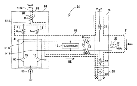
Referring to Fig. 9, a drive circuit 54 includes a resistance (adjusting
resistance)
20 instead of capacitor 19 as compared with drive circuit 53 shown in Fig. 8.
Resistance 20 is connected between the power supply node supplied with power
supply voltage Vcc2 which is a fixed voltage and the connection node between
resistance 11 and resistance 12. Namely, the first end of resistance 11 and
the first
end of resistance 12 are connected to the power supply node with resistance 20
being
interposed. For example, resistance 20 is higher in resistance value than
resistance 11
and resistance 12.
Drive circuit 54 has a path 81 through which bias current Ibias flows. Drive
circuit 54 has a path 82 including a path for supplying modulated current [mod
from
- 23 -
CA 02936736 2016-07-13
output buffer circuit 63 to light-emitting element LD, through which a current
returns
to bias current supply circuit 68 through output buffer circuit 63 from bias
current
supply circuit 68 without going through light-emitting element LD when bias
current
Ibias flows. Drive circuit 54 has a path 83 which is joined to path 82 in
output buffer
circuit 63 and has resistance 20 before a junction, through which a current
flows
through resistance 20 to bias current supply circuit 68 when the bias current
flows.
For example, path 83 is joined to path 82 between resistance 11 and resistance
12.
In other words, with the power supply node supplied with power supply voltage
Vcc2 being defined as one end portion, path 81 and path 82 are separate from
each
other in a stage subsequent to inductor 31 from a state as being joined, and
they run
toward light-emitting element LD and output buffer circuit 63, respectively.
Then,
path 83 is joined to path 82 in output buffer circuit 63, the joined paths are
joined to
path 81 in a stage subsequent to resistance 14 and light-emitting element LD,
and paths
81 to 83 as being joined reach the ground node which is the other end portion,
through
inductor 32 and current source 33.
More specifically, path 81 extends from the power supply node supplied with
power supply voltage Vcc2 successively through inductor 31, light-emitting
element
LD, inductor 32, and current source 33 to the ground node. Path 82 extends
from the
power supply node supplied with power supply voltage Vcc2 successively through
inductor 31, resistance 13, resistance 11, resistance 12, resistance 14,
inductor 32, and
current source 33 to the ground node. Path 83 extends from the power supply
node
supplied with power supply voltage Vcc2 successively through resistance 20,
resistance
12, resistance 14, inductor 32, and current source 33 to the ground node.
Thus, resistances 11 and 12 are DC coupled to the node supplied with the fixed
voltage without light-emitting circuit 75 being interposed. This fixed voltage
is not
limited to power supply voltage Vcc2 and it may be, for example, a ground
voltage.
Namely, a direction of flow of each current is not limited to the above in
optical
transceiver 21, positional relation between the power supply node and the
ground node
can also be reversed such that a direction of flow of each current is reverse
to the above,
- 24 -
CA 02936736 2016-07-13
and a component such as a transistor can also be changed.
Thus, in drive circuit 54, a resistance is connected between the connection
node
between the terminal resistance, of which potential may become unstable in
drive
circuit 52 shown in Fig. 7, and the power supply node.
Thus, the potential at the connection node can be stabilized at a voltage not
higher than power supply voltage Vcc2.
Specifically, a DC impedance Z of a circuit configured with resistance 14,
resistance 12, and resistance 20 is expressed in an equation below, where Rct
represents
a resistance value of resistance 20.
Z = (Rdamp+Rout)xRct/(Rdamp+Rout+Rct)
When Rct is sufficiently greater than (Rdamp+Rout), impedance Z is expressed
in an equation below.
Z = (Rdamp+Rout)
Namely, when resistance 20 is employed instead of capacitor 19 as well, as in
drive circuit 53 shown in Fig. 8, non-effective current INE can be lowered
while
occurrence of ringing due to an unstable potential at the connection node
between
resistance 11 and resistance 12 is suppressed.
Then, temperature dependency of burst response characteristics can be lessened
by not including capacitor 19. Burst response can be faster by not including
capacitor
19.
Drive circuit 54 is not limited to the configuration including only resistance
20
instead of capacitor 19, as compared with drive circuit 53 shown in Fig. 8.
The
configuration should only be such that a resistance is included in a portion
of path 83
before junction with path 82. For example, a series circuit of a resistance
and a
capacitor or a parallel circuit of a resistance and a capacitor may be
provided in that
portion.
Fig. 10 is a diagram showing an equivalent circuit in path 82 and path 83 of
the
drive circuit according to the embodiment of the present invention.
Assuming Rdamp = 0 Pi, Rout = 25 [a], forward voltage Vf of light-emitting
- 25 -
CA 02936736 2016-07-13
element LD = 1.5 [V], and inductor 31 having no resistance component, a
circuit
configured with resistances 11 to 14 and 20 is represented as a parallel
circuit A as
shown in Fig. 10.
Namely, resistance 11 having resistance value Rout and resistance 20 having
resistance value Rct are connected in parallel, and this parallel circuit A
has one end
connected to a node supplied with voltage Vf and the other end connected to
the first
end of resistance 12 having resistance value Rout. The second end of
resistance 12 is
connected to the ground node.
A connection node Nlla between the power supply node supplied with power
supply voltage Vcc2 and resistance 20 and a connection node N11 b between
resistance
11 and resistance 13 in Fig. 9 correspond to a connection node N11 between the
node
supplied with voltage Vf and resistances 11 and 20 in Fig. 10. A connection
node
N12 among resistance 20, resistance 11, and resistance 12 in Fig. 9
corresponds to a
connection node N12 among resistance 20, resistance 11, and resistance 12 in
Fig. 10.
A connection node N13 between resistance 12 and resistance 14 in Fig. 9
corresponds
to a connection node N13 between the ground node and resistance 12 in Fig. 10.
Fig. 11 is a diagram showing relation among resistance value Rct, an impedance
of parallel circuit A, and a non-effective current in the equivalent circuit
shown in Fig.
10.
Referring to Fig. 11, when resistance value Rct is 1000 [pF], that is, a
connection node between the terminal resistances is open in DC manner by
including
capacitor 19 as in the configuration shown in Fig. 8, parallel circuit A has
an
impedance of 25 [0] and non-effective current [NE has magnitude of Vf/combined
resistance of equivalent circuit = 1.5/50=30 [mA]. When resistance value Rct
is 100
[a], parallel circuit A has an impedance of 20 [S2] and non-effective current
INE has
magnitude of Vf/combined resistance of equivalent circuit = 1.5/45 = 33 [mA].
When
resistance value Rct is 37.5 [a], parallel circuit A has an impedance of 15
[a] and non-
effective current INE has magnitude of Vf/combined resistance of equivalent
circuit =
1.5/40 = 37.5 [mA]. When resistance value Rct is 16.7 [0], parallel circuit A
has an
- 26 -
CA 02936736 2016-07-13
impedance of 10 [S2] and non-effective current INE has magnitude of
Vf/combined
resistance of equivalent circuit = 1.5/35 = 42.9 [mA]. When resistance value
Rct is
6.25 [a], parallel circuit A has an impedance of 5 [Q] and non-effective
current INE
has magnitude of Vf/combined resistance of equivalent circuit = 1.5/30 = 50
[mA].
When resistance value Rct is 0 [Q], that is, when resistances 11 and 12 and
the power
supply node supplied with power supply voltage Vcc2 are short-circuited as in
the
configuration shown in Fig. 6, parallel circuit A has an impedance of 0 [Q]
and non-
effective current INE has magnitude of Vf/combined resistance of equivalent
circuit =
1.5/25 = 60 [mA].
With resistance value Rct of 1000 [pF] being defined as the reference, that
is,
0%, a rate of change in non-effective current INE is +10% when resistance
value Rct
is 100 [12], it is +25% when resistance value Rct is 37.5 [Q], it is +43% when
resistance value Rct is 16.7 [0], it is +67% when resistance value Rct is 6.25
[Q], and
it is +100% when resistance value Rct is 0 [0].
With attention being paid to a rate of change in non-effective current, the
drive
circuit according to the embodiment of the present invention can be
implemented so
long as the rate of change is higher than 0% and lower than 100%, with a rate
of change
not lower than 2% and not higher than 70% being preferred, and a rate of
change not
lower than 7% and not higher than 30% being further preferred.
Namely, resistance value Rct of resistance 20 is such a value that a current
which flows through path 83 has magnitude not lower than 2% and not higher
than
70% of magnitude of a current which flows through path 82, that is, a non-
effective
current which flows at the time when no resistance 20 is provided and the
connection
node between resistance 11 and resistance 12 is open in DC manner.
More preferably, resistance value Rct of resistance 20 is such a value that
magnitude of a current which flows through path 83 is not lower than 7% and
not
higher than 30% of magnitude of a current which flows through path 82.
Fig. 12 is a diagram showing a result of measurement of temperature
characteristics of an optical signal output from drive circuit 53.
-27-
CA 02936736 2016-07-13
In Fig. 12, the abscissa represents time and the ordinate represents power. A
column of "burst (pre-bias)" shows an enlarged waveform in a pre-bias section
of a
burst optical signal, that is, after the timing of start of supply of bias
current Ibias and
within a prescribed period of time before the timing of start of supply of
modulated
current Imod. A column of "burst (high level)" shows a waveform with attention
being paid to timing after the timing of start of supply of modulated current
Imod, with
the abscissa being shown as being narrowed as compared with "burst (pre-
bias)". In
"burst (pre-bias)" and "burst (high level)," B represents a portion where an
optical
signal repeats a logic high level and a logic low level. A column of "eye
pattern"
represents an eye pattern of an optical signal.
Scales on the abscissa and the ordinate are the same at each of ¨5 C, 25 C,
and
70 C, and magnitude indicated by each of markers MK1 and MK2 on the ordinate
is
the same.
Fig. 12 shows that a terminal C, that is, capacitor 19, has a capacitance
value of
1000 pF and a bit rate of an optical signal is set to 10.3125 Gbps
(gigabits/second).
Referring to Fig. 12, based on the waveform of "burst (pre-bias)" at each
temperature, a level of a burst optical signal in the pre-bias section lowers
with increase
in temperature. Based on the waveform in "eye pattern" at each temperature, an
extinction ratio at ¨5 C is 6.59 dB, an extinction ratio at 25 C is 6.96 dB,
and an
extinction ratio at 70 C is 7.53 dB. Namely, it can be seen that burst
response
characteristics have temperature dependency.
Fig. 13 is a diagram showing a result of measurement of temperature
characteristics of an optical signal output from drive circuit 53. The figure
is
interpreted similarly to Fig. 12.
Fig. 13 shows that terminal C, that is, capacitor 19, has a capacitance value
of
1000 pF and a bit rate of an optical signal is set to 1.25 Gbps
(gigabits/second).
Referring to Fig. 13, based on the waveform of "burst (pre-bias)" at each
temperature, a level of a burst optical signal in the pre-bias section lowers
with increase
in temperature. Based on the waveform in "eye pattern" at each temperature, an
- 28 -
CA 02936736 2016-07-13
extinction ratio at ¨5 C is 7.68 dB, an extinction ratio at 25 C is 8.16 dB,
and an
extinction ratio at 70 C is 9.62 dB. Namely, it can be seen that burst
response
characteristics have temperature dependency.
Temperature dependency of the extinction ratio shown in Fig. 13 is higher than
temperature dependency of the extinction ratio shown in Fig. 12. This may be
because frequency characteristics of light-emitting element LD appear in a
direction
cancelling temperature dependency of the extinction ratio when the bit rate of
the
optical signal is as high as 10.3125 Gbps. Namely, variation in extinction
ratio from
¨5 C to 70 C is expected to actually be less than approximately 2 dB.
Fig. 14 is a diagram showing a result of measurement of temperature
characteristics of an optical signal output from drive circuit 51. The figure
is
interpreted similarly to Fig. 12.
Fig. 14 shows that a terminal R has 0 0, that is, resistances 11 and 12 and
the
power supply node supplied with power supply voltage Vcc2 are short-circuited
and a
bit rate of an optical signal is set to 10.3125 Gbps.
Referring to Fig. 14, based on the waveform of "burst (pre-bias)" at each
temperature, a level of a burst optical signal in the pre-bias section is
substantially
constant regardless of the temperature. Based on the waveform in "eye pattern"
at
each temperature, an extinction ratio at ¨5 C is 7.14 dB, an extinction ratio
at 25 C is
6.75 dB, and an extinction ratio at 70 C is 6.62 dB. Namely, it can be seen
that
temperature dependency of burst response characteristics is less than in the
case of
burst response characteristics shown in Fig. 12.
In Fig. 14, the extinction ratio is lower with increase in temperature. This
may
be because of influence by frequency characteristics of light-emitting element
LD as
described previously.
Fig. 15 is a diagram showing a result of measurement of temperature
characteristics of an optical signal output from drive circuit 51. The figure
is
interpreted similarly to Fig. 12.
Fig. 15 shows that terminal R has 0 0, that is, resistances 11 and 12 and the
- 29 -
CA 02936736 2016-07-13
power supply node supplied with power supply voltage Vcc2 are short-circuited
and a
bit rate of an optical signal is set to 1.25 Gbps.
Referring to Fig. 15, based on the waveform of "burst (pre-bias)" at each
temperature, a level of a burst optical signal in the pre-bias section is
substantially
constant regardless of the temperature. Based on the waveform in "eye pattern"
at
each temperature, an extinction ratio at ¨5 C is 8.54 dB, an extinction ratio
at 25 C is
8.42 dB, and an extinction ratio at 70 C is 8.50 dB. Namely, it can be seen
that the
extinction ratio is substantially constant regardless of the temperature.
It can thus be demonstrated that the extinction ratio is affected by the
frequency
characteristics of light-emitting element LD in the case shown in Figs. 12 and
14 where
a bit rate of an optical signal is set to 10.3125 Gbps.
In the configuration shown in Figs. 14 and 15, that is, in drive circuit 51,
disadvantageously, non-effective current INE is high and power consumption is
high as
described previously.
Fig. 16 is a diagram showing a summary of results of measurement shown in
Figs. 12 to 15.
Referring to Fig. 16, when terminal C has 1000 pF and a bit rate of an optical
signal is set to 10.3125 Gbps, variation in extinction ratio from ¨5 C to 70 C
is +0.94
dB. When terminal C has 1000 pF and a bit rate of an optical signal is
set to 1.25
Gbps, variation in extinction ratio from ¨5 C to 70 C is +1.94 dB. When
terminal R
has 0 SI and a bit rate of an optical signal is set to 10.3125 Gbps, variation
in extinction
ratio from ¨5 C to 70 C is ¨0.52 dB. When terminal R has 0 and a bit rate of
an
optical signal is set to 1.25 Gbps, variation in extinction ratio from ¨5 C to
70 C is
¨0.04 dB.
In the configuration having terminal R = 0f2, with a bit rate of an optical
signal
= 1.25 Gbps, the extinction ratio does not have temperature dependency,
whereas with
a bit rate of an optical signal = 10.3125 Gbps, the extinction ratio tends to
be lower at a
high temperature.
- 30 -
CA 02936736 2016-07-13
This may be because a time period for rising and falling of an optical signal
is
short at a high temperature.
In the configuration having terminal C = 1000 pF, in any case of bit rates of
an
optical signal = 10.3125 Gbps and 1.25 Gbps, the extinction ratio tends to
increase at a
high temperature and such a tendency is noticeable in particular when the bit
rate is set
to 1.25 Gbps.
With the configuration having terminal R = 0, a level of an optical signal in
the pre-bias section is substantially constant at each temperature, and the
tendency of
increase in extinction ratio at a high temperature is not observed. Therefore,
temperature dependency of the extinction ratio in the configuration having
terminal C =
1000 pF may be because of temperature characteristics of a time constant owing
to
terminal C = 1000 pF.
Fig. 17 is a diagram showing a result of measurement of waveforms of an
optical signal when a capacitance value of capacitor 19 is varied in drive
circuit 53.
The figure is interpreted similarly to Fig. 12. Fig. 17 shows a result of
measurement
at 25 C.
Referring to Fig. 17, in drive circuit 53 including capacitor 19 having a
capacitance value of 1000 pF, no ringing occurs in a rising portion E of a
burst optical
signal.
In contrast, in a configuration of drive circuit 53 from which capacitor 19
has
been removed, that is, in drive circuit 52 shown in Fig. 7, ringing is great
in a rising
portion D1 of a burst optical signal. In a configuration of drive circuit 53
in which
capacitor 19 has a lower capacitance value of 47 pF, similarly, ringing is
great in a
rising portion D2 of a burst optical signal.
Thus, it can be seen that simple removal of capacitor 19 to thereby open the
connection node between the terminal resistances or lowering in capacitance
value of
capacitor 19 is inappropriate, because ringing becomes greater, although burst
response
is faster.
Fig. 18 is a diagram showing a result of measurement of temperature
-31 -
CA 02936736 2016-07-13
characteristics of an optical signal output from drive circuit 54. The figure
is
interpreted similarly to Fig. 12.
Fig. 18 shows that terminal R, that is resistance 20, has a resistance value
of 100
and a bit rate of an optical signal is set to 10.3125 Gbps.
Fig. 19 is a diagram showing a summary of results of measurement shown in
Figs. 12 to 14 and 18.
Referring to Figs. 18 and 19, based on the waveform of "burst (pre-bias)" at
each temperature, an amount of lowering in level of a burst optical signal in
the pre-
bias section due to temperature increase is small. Based on the waveform in
"eye
pattern" at each temperature, an extinction ratio at ¨5 C is 7.00 dB, an
extinction ratio
at 25 C is 6.95 dB, and an extinction ratio at 70 C is 6.81 dB. Namely,
variation in
extinction ratio from ¨5 C to 70 C is as small as ¨0.19 dB, and improvement as
compared to the case shown in Figs. 12 and 14 can be seen.
As shown in Fig. 18, in drive circuit 54, an eye pattern as in Figs. 12 and 14
is
obtained without a waveform of the eye pattern being lost. Namely, it can be
seen
that characteristics in transmission of an optical signal comparable to those
in drive
circuits 51 to 53 shown in Figs. 6 to 8 are obtained in the drive circuit
shown in Fig. 9.
In the burst optical signals shown on an upper side and a lower side of Fig.
17,
ringing is greater in rising portions D1 an D2 of the burst optical signals
than in the
burst optical signal shown in the center in Fig. 17.
In contrast, ringing is less in a rising portion F of the burst optical signal
at each
of ¨5 C, 25 C, and 70 C than in the burst optical signals shown on the upper
side and
the lower side in Fig. 17, and it can be seen that characteristics in
transmission of a
burst optical signal has been improved.
In this measurement, at 70 C shown in Fig. 12 and at 70 C shown in Fig. 18,
currents of 96 mA and 98 mA were consumed in the drive circuits, respectively.
Namely, it can be seen that drive circuit 54 shown in Fig. 9 is lower in rate
of increase
in non-effective current INE and better in terms of power consumption than
drive
circuit 53 shown in Fig. 8.
- 32 -
CA 02936736 2016-07-13
In a configuration with a capacitive element being interposed in a line for a
burst signal such as a laser drive circuit described in PTD 1, the capacitive
element
normally has temperature dependency, and hence burst response characteristics
have
temperature dependency. This temperature dependency may lead to deterioration
in
characteristics in transmission of an optical signal and may adversely affect
communication.
In contrast, in the drive circuit according to the embodiment of the present
invention, bias current supply circuit 68 supplies bias current Ibias to light-
emitting
element LD for transmitting an optical signal. Output buffer circuit 63
supplies to
light-emitting element LD, modulated current Imod having magnitude in
accordance
with a logical value of data to be transmitted. Drive circuit 54 has path 81
through
which bias current Ibias flows. Drive circuit 54 has path 82 which includes a
path for
supplying modulated current Imod to light-emitting element LD from output
buffer
circuit 63, through which a current returns to bias current supply circuit 68
through
output buffer circuit 63 from bias current supply circuit 68 without going
through light-
emitting element LD when bias current Ibias flows. Drive circuit 54 has path
83
which is joined to path 82 in output buffer circuit 63 and has resistance 20
before a
junction, through which a current flows through adjusting resistance 20 to
bias current
supply circuit 68 when bias current Ibias flows.
According to such a configuration, as compared with a configuration in which
only a capacitor is provided in a portion of path 83 before the junction with
path 82,
temperature dependency of burst response characteristics can be lessened and
deterioration in characteristics in transmission of an optical signal can be
suppressed.
Therefore, with the drive circuit according to the embodiment of the present
invention,
temperature dependency in a circuit transmitting an optical signal can be
suppressed
and satisfactory communication can be realized.
In the drive circuit according to the embodiment of the present invention,
resistance 20 has such a resistance value that magnitude of the current which
flows
through path 83 is not lower than 2% and not higher than 70% of magnitude of
the
- 33 -
CA 02936736 2016-07-13
current which flows through path 82.
According to such a configuration, even when path 83 is not DC isolated from
bias current supply circuit 68, a non-effective current which does not
contribute to
drive of the light-emitting element, that is, a current which flows between
path 83 and
bias current supply circuit 68, can be lowered.
In the drive circuit according to the embodiment of the present invention,
output
buffer circuit 63 includes differential drive circuit 41 switched to allow or
not to allow
supply of the current to light-emitting element LD in accordance with the
logical value
of the data and resistance 11 and resistance 12 connected in series between
differential
outputs of differential drive circuit 41. Path 83 is joined to path 82 between
resistance
11 and resistance 12.
Thus, with the configuration including resistance 11 and resistance 12 which
are
terminal resistances, deterioration in characteristics in transmission in
differential drive
circuit 41 can be suppressed in particular in transmission of a high-frequency
optical
signal. In addition, occurrence of ringing due to an unstable potential at a
connection
node between resistance 11 and resistance 12 can be suppressed.
In the drive circuit according to the embodiment of the present invention,
bias
current supply circuit 68 starts supply of bias current Ibias when a
transmission enable
signal for transmitting a burst optical signal is activated.
According to such a configuration, in particular in a circuit which transmits
a
burst optical signal, to which supply of the bias current is started in
response to
activation of a transmission enable signal, a behavior of the circuit at the
time of start of
supply of the bias current can be stabilized.
In the drive circuit according to the embodiment of the present invention, the
optical signal has a bit rate higher than 2.5 gigabits/second.
According to such a configuration, in particular in an optical communication
system in which an optical signal at a high bit rate higher than 2.5
gigabits/second is
transmitted, temperature dependency in a circuit transmitting an optical
signal can be
suppressed and satisfactory communication can be realized.
- 34 -
CA 02936736 2016-07-13
Though the drive circuit according to the embodiment of the present invention
is configured such that differential drive circuit 41 includes a single
transistor circuit,
limitation thereto is not intended. Differential drive circuit 41 may include
a plurality
of stages of transistor circuits. In this case, a DC power supply current
should only be
supplied from light-emitting circuit 75 to the circuit in the last stage.
It should be understood that the embodiment above is illustrative and non-
restrictive in every respect. The scope of the present invention is defined by
the terms
of the claims, rather than the description above, and is intended to include
any
modifications within the scope and meaning equivalent to the terms of the
claims.
The description above includes features additionally described below.
[Additional Aspect 1]
A drive circuit included in an optical network unit adapted to 10G-EPON,
comprising:
a bias current supply circuit for supplying a bias current to a light-emitting
element for transmitting an optical signal; and
a modulated current supply circuit for supplying to the light-emitting
element, a
modulated current having magnitude in accordance with a logical value of data
to be
transmitted, and having
a first path through which the bias current flows,
a second path which includes a path for supplying the modulated current to the
light-emitting element from the modulated current supply circuit, through
which a
current returns to the bias current supply circuit through the modulated
current supply
circuit from the bias current supply circuit without going through the light-
emitting
element when the bias current flows, and
a third path which is joined to the second path in the modulated current
supply
circuit and has an adjusting resistance before a junction, through which a
current flows
through the adjusting resistance to the bias current supply circuit when the
bias current
flows, and
the modulated current supply circuit and the light-emitting element being DC
- 35 -
CA 02936736 2016-07-13
coupled to each other.
[Additional Aspect 2]
An optical network unit used in 10G-EPON in a communication system in
which optical signals from a plurality of optical network units to an optical
line
terminal are time division multiplexed, comprising:
a light-emitting element for transmitting the optical signal; and
a drive circuit for driving the light-emitting element,
the drive circuit including
a bias current supply circuit for supplying a bias current to the light-
emitting element, and
a modulated current supply circuit for supplying to the light-emitting
element, a modulated current having magnitude in accordance with a logical
value of
data to be transmitted, and having
a first path through which the bias current flows,
a second path which includes a path for supplying the modulated current
to the light-emitting element from the modulated current supply circuit,
through which
a current returns to the bias current supply circuit through the modulated
current supply
circuit from the bias current supply circuit without going through the light-
emitting
element when the bias current flows, and
a third path which is joined to the second path in the modulated current
supply circuit and has an adjusting resistance before a junction, through
which a current
flows through the adjusting resistance to the bias current supply circuit when
the bias
current flows, and
the modulated current supply circuit and the light-emitting element being DC
coupled to each other.
REFERENCE SIGNS LIST
11 to 14 resistance; 15, 16 N-type transistor; 17 filter circuit; 19
capacitor; 20
resistance (adjusting resistance); 21 optical transceiver; 22 PON reception
processing
unit; 23 buffer memory; 24 UN transmission processing unit; 25 UN! port; 26 UN
- 36 -
CA 02936736 2016-07-13
reception processing unit; 27 buffer memory; 28 PON transmission processing
unit; 29
control unit; 31, 32 inductor; 33 current source; 41 differential drive
circuit; 51 to 53
drive circuit; 61 pre-buffer circuit; 62 equalizer circuit; 63 output buffer
circuit
(modulated current supply circuit); 64 to 66 power supply; 67 timing circuit;
68 bias
current supply circuit; 69 master I/F (interface); 70 CPU; 71 slave I/F; 72
control
register; 73 storage unit; 75 light-emitting circuit; 81 to 83 path; 201
optical line
terminal; 202A, 202B, 202C, 202D optical network unit; 301 PON system; Cl, C2
capacitor; LD light-emitting element; SP I, SP2 splitter; and OPTF optical
fiber.
-37-