Note: Descriptions are shown in the official language in which they were submitted.
A REMOTELY POWERED, MULTISITE SENSING SYSTEM WITH A SHARED,
TWO-WIRE BUS FOR POWER AND COMMUNICATION
BACKGROUND
[0001] Field of Invention
[0002] The present invention relates generally to a multisite sensing
system with a shared
bus.
[0003] Specifically, the present invention may relate to a remotely
powered, multisite
sensing system with a shared, two-wire bus for power and communication.
[00041 Discussion of the Background
[0005] A conventional implantable analyte sensor may include a single
analyte sensing site
and an antenna that is inductively coupled to an external transceiver and used
solely with the
single analyte sensing site. Such a sensor, when implanted, may provide good
telemetry
coupling with an external transceiver that is worn on the outside of the skin
directly over the
implanted sensor. However, the sensor only has one analyte sensing site and is
dependent upon
having an antenna that can receive power and commands from the external
transceiver at the
same location as the sensing site. These requirements (Le., only one sensing
site and one antenna
per sensing site) may limit the range of applications to which the sensor may
be applied. There
is presently a need in the art for a multisite sensing system.
Date Recue/Date Received 2021-07-30
CA 02936800 2016-07-13
WO 2015/106198 PCT/US2015/011016
SUMMARY
[0006] The present invention overcomes the disadvantages of prior systems
by providing a
multisite sensing system. The multisite sensing system may provide, among
other advantages,
multiple analyte sensing sites and a single interface device (e.g., antenna)
that is shared between
the multiple sensing sites. The multiple sensing sites may include two or more
sensing sites that
detect the same analyte (e.g., for secondary, tertiary, or more detection of
the analyte) and/or one
or more sensing sites that each detect an analyte different than the
analyte(s) detected by the
other sensing site(s) (e.g., for detection of multiple analytes). In addition,
in some embodiments,
the multisite sensing system may include a shared bus (e.g., a two wire
interface), which may
simplify the overall assembly and form factor.
[0007] One aspect of the invention may provide a multisite sensing system
including two or
more analyte sensors, an interface device, and a shared bus. The interface
device may be
configured to receive a power signal and generate power for powering the two
or more analyte
sensors and to convey data signals generated by the two or more analyte
sensors. The shared bus
connected to the interface device and each of the two or more sensors and
configured to provide
the power generated by the interface device to the two or more analyte sensors
and to provide the
data signals generated by the two or more analyte sensors to the interface
device.
[0008] Further variations encompassed within the systems and methods are
described in the
detailed description of the invention below.
BRIEF DESCRIPTION OF THE DRAWINGS
[0009] The accompanying drawings, which are incorporated herein and form
part of the
specification, illustrate various, non-limiting embodiments of the present
invention. In the
drawings, like reference numbers indicate identical or functionally similar
elements.
2
CA 02936800 2016-07-13
WO 2015/106198 PCT/US2015/011016
[0010] FIG. 1 is a schematic view illustrating a multisite sensing system
embodying aspects
of the present invention.
DETAILED DESCRIPTION OF PREFERRED EMBODIMENTS
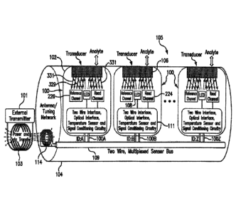
[0011] FIG. 1 is a schematic view of a multisite sensing system 105
embodying aspects of
the present invention. As illustrated in FIG. 1, the multisite sensing system
105 may include a
plurality of analyte sensors 100, a system housing 104, and shared bus 109. In
some non-
limiting embodiments, the multisite sensing system 105 may be a fully
implantable multisite
analyte sensing system. The multisite sensing system 105 may be implanted in a
living animal
(e.g., a living human). The multisite sensing system 105 may be implanted, for
example, in a
living animal's arm, wrist, leg, abdomen, peritoneum, intravenously, or other
region of the living
animal suitable for sensor implantation. For example, in one non-limiting
embodiment, the
multisite sensing system 105 may be implanted beneath the skin (i.e., in the
subcutaneous or
peritoneal tissues). In some embodiments, the multisite sensing system 105 may
be implanted
subcutaneously (e.g., in a location of the body that is appropriate for
subcutaneous measurement
of interstitial fluid glucose), and no portion of the sensor 100 protrudes
from the skin. In some
non-limiting embodiments, the multisite sensing system 105 may be capable of
being
continuously implanted for at least 90 days or longer and may be replaced
thereafter.
[0012] In some embodiments, the multisite sensing system 105 may include
two or more
analyte sensors 100. For example, in the embodiment illustrated in FIG. 1, the
system 105
includes sensors 100A, 100B, and 100Z, but the system 105 may include any
number of sensors
100 greater than or equal to two (e.g., two, three, four, five, ten, etc.).
The analyte sensors 100
may detect the presence, amount, and/or concentration of an analyte (e.g.,
glucose, oxygen,
cardiac markers, low-density lipoprotein (LDL), high-density lipoprotein
(HDL), or
3
CA 02936800 2016-07-13
WO 2015/106198 PCT/US2015/011016
triglycerides). In some embodiments, two or more of the sensors 100 may detect
the same
analyte. In some non-limiting embodiments where two or more of the sensors 100
detect the
same analyte, a voting scheme (e.g., taking an integrated average of the
measurements from the
sensors detecting the same analyte and/or discounting a measurement that is
significantly
different than other measurements of the same analyte) may be used (e.g., by
the transceiver
101). In some embodiments, one or more of the sensors 100 may detect a first
analyte, and
another one or more sensors 100 may detect a second, different analyte. In
some embodiments,
sensors 100 may additionally detect third, fourth, and/or more different
analytes. In some
embodiments, the sensors 100 are spatially separated for analyte detection at
multiple locations.
In some non-limiting embodiments, the analyte sensors 100 may be optical
sensors (e.g.,
fluorometers). In some embodiments, the sensors 100 may be chemical or
biochemical sensors.
[0013] The multisite sensing system 105 may communicate with an external
transceiver 101.
The transceiver 101 may be an electronic device that communicates with the
multisite sensing
system 105 to power the sensors 100 and/or receive measurement information
(e.g.,
photodetector and/or temperature sensor readings) from the sensors 100. The
measurement
information may include one or more readings from one or more photodetectors
of the sensors
100 and/or one or more readings from one or more temperature sensors of the
sensors 100. In
some embodiments, the transceiver 101 may calculate analyte concentrations
from the
measurement information received from the sensor 100. However, it is not
required that the
transceiver 101 perform the analyte concentration calculations itself, and, in
some alternative
embodiments, the transceiver 101 may instead convey/relay the measurement
information
received from the sensor 100 to another device for calculation of analyte
concentrations.
4
CA 02936800 2016-07-13
WO 2015/106198 PCT/US2015/011016
[0014] In some embodiments (e.g., embodiments in which the multisite
sensing system 105
is a fully implantable multisite sensing system), the transceiver 101 may
implement a passive
telemetry for communicating with the implantable sensor 100 via an inductive
magnetic link for
both power and data transfer. The multisite sensing system 105 may include an
inductive
element 114, which may be, for example, a ferrite based micro-antenna. In some
embodiments,
the inductive element 114 may be connected to analyte detection circuitry. For
example, in some
embodiments, where the sensors 100 are optical sensors, the inductive element
114 may be
connected to micro-fluorimeter circuitry (e.g., an application specification
integrated circuit
(ASIC)) and a related optical detection system of the sensor 100. In some
embodiments, the
sensor 100 may not include a battery, and, as a result, the multisite sensing
system 105 may rely
on the transceiver 101 to provide power for the sensors 100 and a data link to
convey analyte-
related data from the sensors 100 to transceiver 101.
[0015] In some non-limiting embodiments, the multisite sensing system 105
may be a
passive, fully implantable multisite sensing system having a small size. For a
multisite sensing
system 105 that is a fully implantable multisite sensing system having no
battery power source,
the transceiver 101 may provide energy to run the sensors 100 of the multisite
sensing system
105 via a magnetic field. In some embodiments, the magnetic transceiver-
sensing system link
can be considered as "weakly coupled transformer" type. The magnetic
transceiver-sensing
system link may provide energy and a link for data transfer using amplitude
modulation (AM).
Although in some embodiments, data transfer is carried out using AM, in
alternative
embodiments, other types of modulation may be used. The magnetic transceiver-
sensor link may
have a low efficiency of power transfer and, therefore, may require relatively
high power
amplifier to energize the sensors 100 of the multisite sensing system 105 at
longer distances. In
CA 02936800 2016-07-13
WO 2015/106198 PCT/US2015/011016
some non-limiting embodiments, the transceiver 101 and multisite sensing
system 105 may
communicate using near field communication (e.g., at a frequency of 13.56MFLz,
which can
achieve high penetration through the skin and is a medically approved
frequency band) for power
transfer. However, this is not required, and, in other embodiments, different
frequencies may be
used for powering and communicating with the sensor 100.
[0016] In some embodiments, as illustrated in FIG. 1, the transceiver 101
may include an
inductive element 103, such as, for example, a coil. The transceiver 101 may
generate an
electromagnetic wave or electrodynamic field (e.g., by using a coil) to induce
a current in an
inductive element 114 of the multisite sensing system 105, which powers the
sensors 100. The
transceiver 101 may also convey data (e.g., commands) to the sensors 100 of
the multisite
sensing system 105. For example, in a non-limiting embodiment, the transceiver
101 may
convey data by modulating the electromagnetic wave used to power the sensors
100 (e.g., by
modulating the current flowing through a coil 103 of the transceiver 101). The
modulation in the
electromagnetic wave generated by the transceiver 101 may be
detected/extracted by the sensors
100. Moreover, the transceiver 101 may receive data (e.g., measurement
information) from the
sensors 100 of the multisite sensing system 105. For example, in a non-
limiting embodiment, the
transceiver 101 may receive data by detecting modulations in the
electromagnetic wave
generated by one or more of the sensors 100, e.g., by detecting modulations in
the current
flowing through the coil 103 of the transceiver 101.
[0017] The inductive element 103 of the transceiver 101 and the inductive
element 114 of the
multisite sensing system 105 may be in any configuration that permits adequate
field strength to
be achieved when the two inductive elements are brought within adequate
physical proximity.
6
CA 02936800 2016-07-13
WO 2015/106198 PCT/US2015/011016
[0018] In some embodiments, the multisite sensing system 105 includes a
shared bus 109
connected to the inductive element 114 and to each of the sensors 100. In some
non-limiting
embodiments, the bus 109 may be a multiplexed bus. In some non-limiting
embodiments, the
bus 109 may be a two wire, multiplexed bus. For example, in one non-limiting
embodiment, the
shared bus 109 may consist of two wires connected to the inductive element
114. A first wire of
the shared bus 109 may be connected to a first end of the inductive element
114 and to a first
input/output port (e.g., a pin) of each of the sensors 100, and a second wire
of the shared bus 109
may be connected to a second end of the inductive element 114 and to a second
input/output port
(e.g., a pin) of each of the sensors 100. In some non-limiting embodiments,
the first and second
input/output ports may be resonant nodes of an LC tank circuit. In some
embodiments, the
shared bus 109 delivers the power generated by the inductive element 114 to
each of the sensors
100. In some embodiments, the connection of the shared bus 109 to the
inductive element 114
facilitates data communication between the sensors 100 and the transceiver
101.
[0019] In some non-limiting embodiments, multiplexing may be performed
using address
mode communication features of the sensors 100 (e.g., address mode
communication features of
bus interface circuitry included in the circuit components 111 of the sensors
100). In some
embodiments, measurement commands conveyed by the inductive element 103 of the
transceiver
101 (e.g., by modulating the electromagnetic wave) may include an address
(e.g., a unique sensor
ID) identifying a particular one of the sensors 100, and the address mode
communication
features of the sensors 100 may extract the address in the conveyed
measurement commands. In
some embodiments, only the sensor 100 to which the measurement command is
addressed (e.g.,
only the sensor 100 whose unique ID matches the unique ID included in the
measurement
command) performs a measurement and provides a response through the passive
interface (e.g.,
7
CA 02936800 2016-07-13
WO 2015/106198 PCT/US2015/011016
by modulating in the electromagnetic wave). In this way, sensors 100 connected
to the shared
bus 109 may operate in a multiplexed fashion. Although one example for
multiplexed operation
of the sensors 100 is provided above, alternative embodiments may achieve
multiplexed sensor
operation in one or more different fashions. For example, in some alternative
embodiments, the
sensors 100 may be configured to use an anti-collision algorithm for
multiplexing the response
on the shared antenna 114. In some non-limiting embodiments, the two wires of
the shared bus
109 may enable the single inductive element 114 (e.g., a single antenna) to
interface with
multiple sensors 100, which may be spatially separated for analyte
detection/transduction at
multiple locations.
[0020] In some non-limiting embodiments, as illustrated in FIG. 1, the
sensors 100, shared
bus 109, and inductive element 114 may be encased in a system housing 104
(i.e., body, shell,
capsule, or encasement), which may be rigid and biocompatible. In one non-
limiting
embodiment, the system housing 104 may be a silicon tube. However, this is not
required, and,
in other embodiments, different materials and/or shapes may be used for the
system housing 104.
[0021] The sensors 100 may include a transmissive optical cavity 102. In
some non-limiting
embodiments, the transmissive optical cavity 102 may be formed from a
suitable, optically
transmissive polymer material, such as, for example, acrylic polymers (e.g.,
polymethylmethacrylate (PMMA)). However, this is not required, and, in other
embodiments,
different materials may be used for the transmissive optical cavity 102.
[0022] In some embodiments, the sensors 100 may include an analyte
indicator element 106,
such as, for example, a polymer graft coated, diffused, adhered, or embedded
on or in at least a
portion of the exterior surface of the system housing 104. The analyte
indicator element 106
(e.g., polymer graft) of the sensor 100 may include indicator molecules (e.g.,
fluorescent
8
CA 02936800 2016-07-13
WO 2015/106198 PCT/US2015/011016
indicator molecules) exhibiting one or more detectable properties (e.g.,
optical properties) based
on the amount or concentration of the analyte in proximity to the analyte
indicator element. In
some embodiments, the sensors 100 may include a light source 108 that emits
excitation light
329 over a range of wavelengths that interact with the indicator molecules in
the analyte
indicator element 106. The sensors 100 may also include one or more
photodetectors 224,226
(e.g., photodiodes, phototransistors, photoresistors, or other photosensitive
elements). The one
or more photodetectors (e.g., photodetector 224) may be sensitive to emission
light 331 (e.g.,
fluorescent light) emitted by the indicator molecules of the analyte indicator
element 106 such
that a signal generated by a photodetector (e.g., photodetector 224) in
response thereto that is
indicative of the level of emission light 331 of the indicator molecules and,
thus, the amount of
analyte of interest (e.g., glucose). In some non-limiting embodiments, one or
more of the
photodetectors (e.g., photodetector 226) may be sensitive to excitation light
329 that is reflected
from the analyte indicator element 106. In some non-limiting embodiments, one
or more of the
photodetectors may be covered by one or more filters that allow only a certain
subset of
wavelengths of light to pass through (e.g., a subset of wavelengths
corresponding to emission
light 331 or a subset of wavelengths corresponding to reflected excitation
light) and reflect the
remaining wavelengths. In some non-limiting embodiments, the sensors 100 may
include a
temperature transducer. In some non-limiting embodiments, the multisite
sensing system 105
may include a drug-eluting polymer matrix that disperses one or more
therapeutic agents (e.g., an
anti-inflammatory drug).
[0023] In some embodiments, the sensors 100 may include circuit components
111. In some
non-limiting embodiments, the circuit components 111 may include a bus
interface, optical
interface, temperature sensor, analog-to-digital converter, and/or signal
conditioning circuitry. In
9
CA 02936800 2016-07-13
WO 2015/106198 PCT/US2015/011016
some non-limiting embodiments, the bus interface may perform the address mode
communication described above. In some of these address mode communication
embodiments,
all of the sensors 100 may receive a measurement command, and only the sensor
100 to which
the measurement command is addressed responds to the measurement command via
the bus 109
and shared inductive element 114.
10024] In some embodiments, the sensors 100 may include a substrate. In
some
embodiments, the substrate may be a circuit board (e.g., a printed circuit
board (PCB) or flexible
PCB) on which one or more of circuit components 111 (e.g., analog and/or
digital circuit
components) may be mounted or otherwise attached. However, in some alternative
embodiments, the substrate may be a semiconductor substrate having one or more
of the circuit
components 111 fabricated therein. For instance, the fabricated circuit
components may include
analog and/or digital circuitry. Also, in some semiconductor substrate
embodiments, in addition
to the circuit components fabricated in the semiconductor substrate, circuit
components may be
mounted or otherwise attached to the semiconductor substrate. In other words,
in some
semiconductor substrate embodiments, a portion or all of the circuit
components 111, which may
include discrete circuit elements, an integrated circuit (e.g., an application
specific integrated
circuit (ASIC)) and/or other electronic components (e.g., a non-volatile
memory), may be
fabricated in the semiconductor substrate with the remainder of the circuit
components 111 is
secured to the semiconductor substrate, which may provide communication paths
between the
various secured components.
[0025] In some embodiments, the one or more of the analyte indicator
element 106, light
source 108, photodetectors 224, 226, circuit components 111, and substrate of
the sensors 100
may include some or all of the features described in one or more of U.S.
Application Serial No.
13/761,839, filed on February 7, 2013, U.S. Application Serial No. 13/937,871,
filed on July 9,
2013, U.S. Application Serial No. 13/650,016, filed on October 11,2012, and
U.S. Application
Serial No. 14/142,017, filed on December 27, 2013. Similarly, the structure,
function, and/or
features of the system housing 104, sensors 100, and/or transceiver 101 may be
as described in
one or more of U.S. Application Serial Nos. 13/761,839, 13/937,871,
13/650,016, and
14/142,017. For instance, the system housing 104 may have one or more
hydrophobic,
hydrophilic, opaque, and/or immune response blocking membranes or layers on
the exterior
thereof.
[0026] Although
in some embodiments, as illustrated in Fig. 1, the sensors 100 may be an
optical sensors, this is not required, and, in one or more alternative
embodiments, sensors 100
may be a different types of analyte sensors, such as, for example, diffusion
sensors or pressure
sensors. Also, although in some embodiments, as illustrated in Fig. 1, the
multisite sensing
system 105 may be a fully implantable sensing system, this is not required,
and, in some
alternative embodiments, the multisite sensing system 105 may be a
transcutaneous sensing
system having a wired connection to the transceiver 101. For example, in some
alternative
embodiments, the sensing system 105 may be located in or on a transcutaneous
needle (e.g., at
the tip thereof). In these embodiments, instead of wirelessly communicating
using inductive
elements 103 and 114, the multisite sensing system 105 and transceiver 101 may
communicate
using one or more wires connected between the transceiver 101 and the
transceiver
transcutaneous needle that includes the multisite sensing system 105. For
another example, in
some alternative embodiments, the multisite sensing system 105 may be located
in a catheter
(e.g., for intravenous blood glucose monitoring) and may communicate
(wirelessly or using
wires) with the transceiver 101.
II
Date Recue/Date Received 2021-07-30
CA 02936800 2016-07-13
WO 2015/106198 PCT/US2015/011016
[0027] In some embodiments, the multisite sensing system 105 may include a
transceiver
interface device. In some embodiments where the multisite sensing system 105
includes an
antenna (e.g., inductive element 114), the transceiver interface device may
include the antenna
(e.g., inductive element 114) of multisite sensing system 105. In some of the
transcutaneous
embodiments where there exists a wired connection between the multisite
sensing system 105
and the transceiver 101, the transceiver interface device may include the
wired connection.
[0028] Embodiments of the present invention have been fully described above
with reference
to the drawing figures. Although the invention has been described based upon
these preferred
embodiments, it would be apparent to those of skill in the art that certain
modifications,
variations, and alternative constructions could be made to the described
embodiments within the
spirit and scope of the invention.
12