Note: Descriptions are shown in the official language in which they were submitted.
CA 2,936,925
Blakes Ref: 13592/00001
1 ELECTRONIC DEVICE AND POWER ADAPTER
2
3 TECHNICAL FIELD
4 [0001] The present disclosure generally relates to the charging
technical field, and more
particularly, to an electronic device and a power adapter.
6
7 BACKGROUND
8 [0002] Currently, most electronic devices charge a battery by
acquiring direct current
9 from a power adapter through a communication interface thereof. However,
in the related art, in
order to reduce charging time during charging the battery, the charging
current may be enhanced
11 by the power adapter to realize an aim of performing a quick charging on
the battery. However,
12 when charging the battery either in a conventional constant voltage mode
or with increased
13 charging current, if a charging current and/or charging voltage of the
battery is too high during
14 the charging, the battery will be damaged due to overvoltage and/or
overcurrent charging.
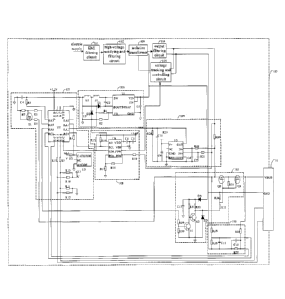
Therefore, in the related art, an overcurrent protection and/or an overvoltage
protection cannot be
16 realized for the battery when the power adapter performs a conventional
charging or quick
17 charging on the battery in the electronic device.
18
19 SUMMARY
[0003] An embodiment of the present disclosure provide a power adapter, so
as to solve a
21 problem in the related art that an overcurrent protection and/or an
overvoltage protection cannot
22 be realized for a battery when the power adapter performs a conventional
charging or quick
23 charging on the battery in the electronic device.
24 [0004] An embodiment of the present disclosure is realized as
follows. There is provided
a power adapter, including a communication interface through which the power
adapter charges a
26 battery in an electronic device and performs a data communication with
the electronic device.
27 The power adapter includes an EMI (Electro-Magnetic Interference) filter
circuit, a high-voltage
28 rectifying and filtering circuit, an isolation transformer, an output
filtering circuit, and a voltage
29 tracking and controlling circuit;
1
23182206.2
CA 2936925 2018-07-23
CA 2,936,925
Blakes Ref: 13592/00001
1 [0095] The power adapter further includes a power circuit, a main
control circuit, a
2 potential adjusting circuit, a current detection circuit, a voltage
detection circuit and an output
3 switch circuit.
4 [0006] An input end of the power circuit is connected with a
secondary end of the
isolation transformer; a power end of the main control circuit, a power end of
the potential
6 .. adjusting circuit and a power end of the current detection circuit are
collectively connected with
7 an output end of the power circuit; both a high-level end of the main
control circuit and a
8 high-level end of the potential adjusting circuit are connected with a
positive output end of the
9 output filtering circuit; a potential adjusting end of the potential
adjusting circuit is connected
with the voltage tracking and controlling circuit; a direct current input end
of the current
11 detection circuit is connected with the positive output end of the
output filtering circuit; a current
12 feedback end of the current detection circuit is connected with a
current detecting end of the
13 .. main control circuit; a clock output end of the main control circuit is
connected with a clock
14 output end of the potential adjusting circuit; a data output end of the
main control circuit is
connected with a data input end of the potential adjusting circuit; a first
detecting end and a
16 second detecting end of the voltage detection circuit are connected with
a direct current output
17 end of the current detection circuit and a negative output end of the
output filtering circuit
18 .. respectively; a first output end and a second output end of the voltage
detection circuit are
19 connected with a first voltage detecting end and a second voltage
detecting end of the main
control circuit respectively; an input end of the output switch circuit is
connected with the direct
21 current output end of the current detection circuit; an output end of
the output switch circuit and
22 the negative output end of the output filtering circuit are connected
with the communication
23 interface; and the output end of the output switch circuit is connected
with a third detecting end
24 of the voltage detection circuit; a ground end of the output switch
circuit is connected with the
negative output end of the output filtering circuit; a controlled end of the
output switch circuit is
26 connected with a switching control end of the main control circuit; a
power end of the output
27 .. switch circuit is connected with the secondary end of the isolation
transformer; each of the
28 negative output end of the output filtering circuit, the output end of
the output switch circuit and
29 a first communication end and a second communication end of the main
control circuit is
2
23182206.2
CA 2936925 2018-07-23
CA 2,936,925
Blakes Ref: 13592/00001
1 connected with the communication interface.
2 [0007] The power circuit obtains power supply from the isolation
transformer and
3 provides the power supply for the main control circuit, the potential
adjusting circuit and the
4 current detection circuit; the potential adjusting circuit drives the
voltage tracking and controlling
circuit to adjust an output voltage of the isolation transformer according to
a control signal sent
6 .. by the main control circuit; the current detection circuit detects an
output current of the power
7 adapter and feeds back a current detecting signal to the main control
circuit, and the voltage
8 detection circuit detects an output voltage of the power adapter and
feeds back a voltage
9 detecting signal to the main control circuit; the output switch circuit
turns on or off a direct
current output of the power adapter according to a switching control signal
sent by the main
11 control circuit.
12 [0008] When a conventional charging or a quick charging is
performed on the battery in
13 the electronic device, the main control circuit determines whether the
output current of the power
14 adapter is greater than a current threshold according to the current
detecting signal and
determines whether the output voltage of the power adapter is greater than a
voltage threshold
16 according to the voltage detecting signal; if the output current of the
power adapter is greater
17 than the current threshold and/or the output voltage of the power
adapter is greater than the
18 voltage threshold, the main control circuit controls the output switch
circuit to turn off the direct
19 current output of the power adapter.
[0009] During the data communication between the main control circuit and
the
21 electronic device, if the electronic device determines that the output
current of the power adapter
22 is greater than the current threshold and/or the output voltage of the
power adapter is greater than
23 the voltage threshold, and feeds back a charging stop instruction to the
main control circuit, the
24 main control circuit controls the output switch circuit to turn off the
direct current output of the
power adapter according to the charging stop instruction.
26 [0010] An embodiment of the present disclosure is to provide an
electronic device,
27 including a battery and further provided with the power adapter
described above.
28 [0011] In at least one embodiment of the present disclosure, the
power adapter including
29 the power circuit, the main control circuit, the potential adjusting
circuit, the current detection
3
23182206.2
CA 2936925 2018-07-23
CA 2,936,925
Blakes Ref: 13592/00001
1 circuit, the voltage detection circuit and the output switch circuit is
provided for the electronic
2 device. The main control circuit determines whether the output current of
the power adapter is
3 greater than the current threshold, and determines whether the output
voltage of the power
4 adapter is greater than the voltage threshold. If the output current is
greater than the current
threshold and/or the output voltage is greater than the voltage threshold, the
main control circuit
6 controls the output switch circuit to turn off the direct current output
of the power adapter. In
7 addition, if the electronic device determines that an overcurrent and/or
overvoltage occurs in the
8 output of the power adapter, and feeds back the charging stop instruction
to the main control
9 circuit, the main control circuit controls the output switch circuit to
turn off the direct current
output of the power adapter according to the charging stop instruction, such
that the overcurrent
11 and/or overvoltage protection is realized for the battery.
12
13 BRIEF DESCRIPTION OF THE DRAWINGS
14 [0012] Fig. 1 is a block diagram of a power adapter provided by
an embodiment of the
present disclosure.
16 [0013] Fig. 2 is a schematic circuit diagram of a power adapter
provided by an
17 embodiment of the present disclosure.
18
19 DETAILED DESCRIPTION
[0014] To make objectives, technical solutions, and advantages of
embodiments of the
21 present invention clearer, the technical solutions in embodiments of the
present invention are
22 hereinafter described clearly and completely with reference to the
accompanying drawings in
23 embodiments of the present invention. It should be understood that, the
specific embodiments
24 described herein are merely used for explanation, but not used to limit
the present disclosure.
[0015] Fig. 1 is a block diagram of a power adapter provided by an
embodiment of the
26 present disclosure. For illustration purposes, only parts related to
embodiments of the present
27 disclosure are shown, which will be described in detail in the
following.
28 [0016] The power adapter 100 provided by an embodiment of the
present disclosure
29 includes a communication interface 10, the power adapter 100 charges a
battery 201 in an
4
23182206.2
CA 2936925 2018-07-23
CA 2,936,925
Biakes Ref: 13592/00001
1 electronic device 200 and performs a data communication with the
electronic device 200 through
2 the communication interface 10.
3 [0017] The power adapter 100 includes an EMI filtering circuit
101, a high-voltage
4 rectifying and filtering circuit 102, an isolation transformer 103, an
output filtering circuit 104
and a voltage tracking and controlling circuit 105. After an electromagnetic
interference filtering
6 is performed on the electric supply by the EMI filtering circuit 101, the
high-voltage rectifying
7 and filtering circuit 102 performs a rectifying and filtering process and
outputs a high-voltage
8 direct current, which is outputted to the output filtering circuit 104
after the electrical isolation in
9 the isolation transformer 103, for being filtered and used to charge the
battery 201. The voltage
tracking and controlling circuit 105 adjusts an output voltage of the
isolation transformer 103
11 according to an output voltage of the output filtering circuit 104.
12 [0018] The power adapter 100 further includes: a power circuit
106, a main control
13 circuit 107, a potential adjusting circuit 108, a current detection
circuit 109, a voltage detection
14 circuit 110 and an output switch circuit 111.
[0019] Please refer to Fig. 1 and Fig. 2, an input end of the power circuit
106 is
16 connected with a secondary end of the isolation transformer 103. A power
end of the main
17 control circuit 107, a power end of the potential adjusting circuit 108
and a power end of the
18 current detection circuit 109 are collectively connected with an output
end of the power circuit
19 106. Both a high-level end of the main control circuit 107 and a high-
level end of the potential
adjusting circuit 108 are connected with a positive output end of the output
filtering circuit 104.
21 The high-level end of the main control circuit 107 is connected with the
positive output end of
22 the output filtering circuit 104 via a second end of the twentieth
resistor R20 (i.e., a direct current
23 output end of the current detection circuit 109). A potential adjusting
end of the potential
24 adjusting circuit 108 is connected with the voltage tracking and
controlling circuit 105. A direct
current input end of the current detection circuit 109 is connected with the
positive output end of
26 the output filtering circuit 104. A current feedback end of the current
detection circuit 109 is
27 connected with a current detecting end of the main control circuit 107.
A clock output end of the
28 main control circuit 107 is connected with a clock input end of the
potential adjusting circuit 108.
29 A data output end of the main control circuit 107 is connected with a
data input end of the
5
23182206.2
CA 2936925 2018-07-23
CA 2,936,925
Blakes Ref: 13592/00001
1 potential adjusting circuit 108. A first detecting end and a second
detecting end of the voltage
2 detection circuit 110 are connected with the direct current output end of
the current detection
3 circuit 109 and a negative output end of the output filtering circuit 104
respectively. A first
4 output end and a second output end of the voltage detection circuit 110
are connected with a first
voltage detecting end and a second voltage detecting end of the main control
circuit 107
6 respectively. An input end of the output switch circuit 111 is connected
with the direct current
7 output end of the current detection circuit 109; and an output end of the
output switch circuit 111
8 is connected with a third detecting end of the voltage detection circuit
110. A ground end of the
9 output switch circuit 111 is connected with the negative output end of
the output filtering circuit
104. A controlled end of the output switch circuit 111 is connected with a
switching control end
11 of the main control circuit 107. A power end of the output switch
circuit 111 is connected with
12 the secondary end of the isolation transformer 103. Each of the negative
output end of the output
13 filtering circuit 104, the output end of the output switch circuit 111
and a first communication
14 end and a second communication end of the main control circuit 107 is
connected with the
communication interface 10 of the power adapter 100.
16 [0020] The power circuit 106 obtains power supply from the
isolation transformer 103
17 and provides the power supply for the main control circuit 107, the
potential adjusting circuit 108
18 and the current detection circuit 109; when a quick charging is
performed on the battery 201 in
19 the electronic device 200, the potential adjusting circuit 108 drives
the voltage tracking and
controlling circuit 105 to adjust an output voltage of the isolation
transformer 103 according to a
21 control signal sent by the main control circuit 107; the current
detection circuit 109 detects an
22 output current of the power adapter 100 and feeds back a current
detecting signal to the main
23 control circuit 107, and the voltage detection circuit 110 detects an
output voltage of the power
24 adapter 100 and feeds back a voltage detecting signal to the main
control circuit 107; the output
switch circuit 111 turns on or off a direct current output of the power
adapter 100 according to a
26 switching control signal sent by the main control circuit 107.
27 [0021] When a conventional charging or a quick charging is
performed on the battery
28 201 in the electronic device 200, the main control circuit 107
determines whether the output
29 current of the power adapter 100 is greater than a current threshold
according to the current
6
23182206.2
CA 2936925 2018-07-23
CA 2,936,925
Blakes Ref: 13592/00001
1 detecting signal, and determines whether the output voltage of the power
adapter 100 is greater
2 than a voltage threshold according to the voltage detecting signal; if
the output current of the
3 power adapter 100 is greater than the current threshold and/or the output
voltage of the power
4 adapter 100 is greater than the voltage threshold, the main control
circuit 107 controls the output
switch circuit 111 to turn off the direct current output of the power adapter
100.
6 [0022] During the data communication between the main control
circuit 107 and the
7 electronic device 200, if the electronic device 200 determines that the
output current of the power
8 adapter 100 is greater than the current threshold and/or the output
voltage of the power adapter
9 100 is greater than the voltage threshold, and feeds back a charging stop
instruction to the main
control circuit 107, the main control circuit 107 controls the output switch
circuit 111 to turn off
11 the direct current output of the power adapter 100 according to the
charging stop instruction.
12 [0023] In at least one embodiment, the data communication between
the main control
13 circuit 107 and the electronic device 200 is performed during the
charging. During this process,
14 either in the conventional charging mode or in the quick charging mode,
the main control circuit
107 would send the output current and output voltage of the power adapter 100
to the electronic
16 device 200. The electronic device 200 determines according to the output
current and output
17 voltage of the power adapter 100 whether an overcurrent and/or
overvoltage occur during the
18 charging. The determine process is the same as the process in which the
main control circuit 107
19 determines the output current and output voltage of the power adapter
100, such that the
electronic device 200 may feedback a charging stop instruction for informing
the main control
21 circuit 107 of turning off the direct current output of the power
adapter 100 when the electronic
22 device 200 determines that an overcurrent and/or overvoltage occurs in
the output of the power
23 adapter 100. Moreover, the electronic device 200 may close its
communication interface actively
24 when determining that an overcurrent and/or overvoltage occurs in the
output of the power
adapter 100, so as to disconnect from the power adapter 100, such that the
overcurrent and/or
26 overvoltage protection may be realized actively.
27 [0024] Fig. 2 is a schematic circuit diagram of a power adapter
provided by an
28 embodiment of the present disclosure. For illustration purposes, only
parts related to
29 embodiments of the present disclosure are shown, which will be described
in detail in the
7
23182206.2
CA 2936925 2018-07-23
CA 2,936,925
Blakes Ref: 13592/00001
1 following.
2 [0025] The power circuit 106 includes: a first capacitor Cl, a
voltage stabilizing chip Ul,
3 a second capacitor C2, a first inductor Li, a second inductor L2, a fist
diode D1, a second diode
4 D2, a third capacitor C3, a first resistor R1 and a second resistor R2.
[0026] A collective node of a first end of the first capacitor Cl, an input
power pin Vin
6 and an enable pin EN of the voltage stabilizing chip U1 is configured as
the input end of the
7 power circuit 106. A second end of the first capacitor Cl and a ground
pin GND of the voltage
8 stabilizing chip Ul are collectively grounded. A switch pin SW of the
voltage stabilizing chip Ul
9 and a first end of the second capacitor C2 are collectively connected
with a first end of the first
inductor LL An inside switch pin BOOST of the voltage stabilizing chip U1 and
a second end of
11 the second capacitor C2 are collectively connected with a cathode of the
first diode Dl. A
12 feedback voltage pin FB of the voltage stabilizing chip U1 is connected
with a first end of the
13 first resistor R1 and a first end of the second resistor R2
respectively. A second end of the first
14 inductor Ll and a cathode of the second diode D2 are collectively
connected with a first end of
the second inductor. A collective node formed by collectively connecting a
second end of the
16 second inductor L2, an anode of the first diode D1, a second end of the
first resistor R1 and a
17 first end of the third capacitor C3 is configured as the output end of
the power circuit 106. An
18 anode of the second diode D2, a second end of the second resistor R2 and
a second end of the
19 third capacitor C3 are collectively grounded. After using the voltage
stabilizing chip Ul as a core
to perform a voltage converting process on a voltage at the secondary end of
the isolation
21 transformer 103, the power circuit 106 outputs the voltage of +3.3V for
providing power supply
22 for the main control circuit 107, the potential adjusting circuit 108
and the current detection
23 circuit 109. In an embodiment, the voltage stabilizing chip U1 is a buck
DC/DC converter with a
24 Model No. MCP16301.
[0027] The main control circuit 107 includes: a main control chip U2, a
third resistor R3,
26 a reference voltage chip U3, a fourth resistor R4, a fifth resistor R5,
a fourth capacitor C4, a sixth
27 resistor R6, a seventh resistor R7, a first NMOS (Negative channel-Metal-
Oxide-Semiconductor)
28 transistor Q1, an eighth resistor R8, a ninth resistor R9, a tenth
resistor R10, an eleventh resistor
29 R11, a twelfth resistor R12, a thirteenth resistor R13 and a fourteenth
resistor R14.
8
23182206.2
CA 2936925 2018-07-23
CA 2,936,925
Blakes Ref: 13592/00001
1 [0028] A power pin VDD of the main control chip U2 is configured
as the power end of
2 the main control circuit 107. A ground pin VSS of the main control chip
U2 is grounded. A first
3 input/output pin RAO of the main control chip U2 is suspended. A first
end of the third resistor
4 R3 is connected with the power pin VDD of the main control chip U2. A
second end of the third
resistor R3 and a first end of the fourth resistor R4 are collectively
connected with a cathode
6 CATHODE of the reference voltage chip U3. An anode ANODE of the reference
voltage chip
7 U3 is grounded. A vacant pin NC of the reference voltage chip U3 is
suspended. A second end of
8 the fourth resistor R4 is connected with a second input/output pin RA1 of
the main control chip
9 U2. A third input/output pin RA2 of the main control chip U2 is
configured as the current
detecting end of the main control circuit 107. A fourth input/output pin RA3
of the main control
11 chip U2 is connected with a first end of the fifth resistor R5. A second
end of the fifth resistor R5
12 and a first end of the fourth capacitor C4 are collectively connected
with the power pin VDD of
13 the main control chip U2. A second end of the fourth capacitor C4 is
grounded. A fifth
14 input/output pin RA4 of the main control chip U2 is configured as the
switching control end of
the main control circuit 107. A sixth input/output pin RA5 of the main control
chip U2 is
16 connected with a first end of the sixth resistor R6. A second end of the
sixth resistor R6 and a
17 grid electrode of the first NMOS transistor Q1 are collectively
connected with a first end of the
18 seventh resistor R7. A second end of the seventh resistor R7 and a
source electrode of the first
19 NMOS transistor 01 are collectively grounded. A drain electrode of the
first NMOS transistor
Q1 is connected with a first end of the eighth resistor R8. A second end of
the eighth resistor R8
21 is configured as the high-level end of the main control circuit 107. A
seventh input/output pin
22 RCO and an eighth input/output pin RC1 of the main control chip U2 are
configured as the clock
23 output end and the data output end of the main control circuit 107
respectively. A ninth
24 input/output pin RC2 and a tenth input/output pin RC3 of the main
control chip U2 are
configured as the first voltage detecting end and the second voltage detecting
end of the main
26 control circuit 107 respectively. An eleventh input/output pin RC4 and a
twelfth input/output pin
27 RC5 of the main control chip U2 are connected with a first end of the
ninth resistor R9 and a first
28 end of the tenth resistor R10 respectively. A first end of the eleventh
resistor R11 and a first end
29 of the twelfth resistor R12 are connected with a second end of the ninth
resistor R9 and a second
9
23182206.2
CA 2936925 2018-07-23
CA 2,936,925
Blakes Ref: 13592/00001
1 end of the tenth resistor R10 respectively. A second end of the eleventh
resistor R11 and a
2 second end of the twelfth resistor R12 are collectively grounded. A first
end of the thirteenth
3 resistor R13 and a first end of the fourteenth resistor R14 are connected
with the second end of
4 the ninth resistor R9 and the second end of the tenth resistor R10
respectively. A second end of
the thirteenth resistor R13 and a second end of the fourteenth resistor R14
are collectively
6 connected with the power pin VDD of the main control chip U2. The second
end of the ninth
7 resistor R9 and the second end of the tenth resistor R10 are configured
as the first
8 communication end and the second communication end of the main control
circuit 107
9 respectively. In an embodiment, the main control chip U2 is a single chip
microcomputer with a
Model No. PIC12LF1822, PIC12F1822, PIC16LF1823 or PIC16F1823, and the
reference
11 voltage chip U3 is a voltage reference device with a Model No. LM4040.
12 [0029] The potential adjusting circuit 108 includes: a fifteenth
resistor R15, a sixteenth
13 resistor R16, a digital potentiometer U4, a seventeenth resistor R17, an
eighteenth resistor R18, a
14 fifth capacitor C5, a sixth capacitor C6 and a nineteenth resistor R19.
[0030] A collective node of a first end of the fifteenth resistor R15, a
first end of the
16 sixteenth resistor R16, a power pin VDD of the digital potentiometer U4
and a first end of the
17 fifth capacitor C5 is configured as the power end of the potential
adjusting circuit 108. A second
18 end of the fifth capacitor C5, a first end of the sixth capacitor C6, a
ground pin VSS of the digital
19 potentiometer U4 and a first end of the seventeenth resistor R17 are
collectively grounded. A
second end of the sixth capacitor C6 is connected with the power pin VDD of
the digital
21 potentiometer U4. A collective node between a second end of the
fifteenth resistor R15 and a
22 serial data pin SDA of the digital potentiometer U4 is configured as the
data input end of the
23 potential adjusting circuit 108. A collective node between a second end
of the sixteenth resistor
24 R16 and a clock input pin SCL of the digital potentiometer U4 is
configured as the clock input
end of the potential adjusting circuit 108. An address zero pin AO of the
digital potentiometer U4
26 is grounded. A first potential wiring pin POA of the digital
potentiometer U4 and a first end of
27 the eighteenth resistor R18 are collectively connected with a second end
of the seventeenth
28 resistor R17. A second end of the eighteenth resistor R18 and a second
potential wiring pin POB
29 of the digital potentiometer U4 are collectively connected with a first
end of the nineteenth
23182206.2
CA 2936925 2018-07-23
CA 2,936,925
Blakes Ref: 13592/00001
1 resistor R19. A second end of the nineteenth resistor R19 is configured
as the high-level end of
2 potential adjusting circuit 108. A potential tap pin POW of the digital
potentiometer U4 is
3 configured as the potential adjusting end of the potential adjusting
circuit 108. The digital
4 potentiometer U4 adjusts an internal sliding variable resistor according
to the clock signal and
the data signal outputted by the main control chip U2, such that the potential
at the tap end of the
6 internal sliding variable resistor (i.e., the potential tap pin POW of
the digital potentiometer U4)
7 is changed, and then the voltage tracking and controlling circuit 105
adjusts the output voltage of
8 the isolation transformer 103 by following the potential changes. The
digital potentiometer U4
9 may be a digital potentiometer with a Model No. MCP45X1.
[0031] The current detection circuit 109 includes : a twentieth resistor
R20, a twenty-first
11 resistor R21, a twenty-second resistor R22, a seventh capacitor C7, an
eighth capacitor C8, a
12 current detection chip U5, a twenty-third resistor R23, a ninth
capacitor C9, a tenth capacitor
13 C10 and a twenty-fourth resistor R24.
14 [0032] A first end and a second end of the twentieth resistor R20
are configured as the
direct current input end and the direct current output end of the current
detection circuit 109
16 respectively. A first end of the twenty-first resistor R21 and a first
end of the twenty-second
17 resistor R22 are connected with a first end and a second end of the
twentieth resistor R20
18 respectively. A second end of the twenty-first resistor R21 and a first
end of the seventh
19 capacitor C7 are collectively connected with a positive input pin IN+ of
the current detection
chip U5. A second end of the twenty-second resistor R22 and a first end of the
eighth capacitor
21 C8 are collectively connected with a negative input pin IN- of the
current detection chip U5. A
22 collective node between a power pin V+ of the current detection chip U5
and a first end of the
23 ninth capacitor C9 is configured as the power end of the current
detection circuit 109. A vacant
24 pin NC of the current detection chip U5 is suspended. An output pin OUT
of the current
detection chip U5 is connected with a first end of the twenty-third resistor
R23. A second end of
26 the twenty-third resistor R23 is configured as the current feedback end
of the current detection
27 circuit 109. A first end of the tenth capacitor C10 and a first end of
the twenty-fourth resistor
28 R24 are collectively connected with the second end of the twenty-third
resistor R23. A second
29 end of the seventh capacitor C7, a second end of the eighth capacitor
C8, a second end of the
11
23182206.2
CA 2936925 2018-07-23
CA 2,936,925
Blakes Ref: 13592/00001
1 ninth capacitor C9, a second end of the tenth capacitor C10, a second end
of the twenty-fourth
2 resistor R24, a ground pin GND, a first reference voltage pin REF1 and a
second reference
3 voltage pin REF2 of the current detection chip U5 are collectively
grounded. The twentieth
4 resistor 20 used as a current detecting resistor samples the output
current of the output filtering
circuit 104 (i.e., the output current of the power adapter 100), and then the
current detecting
6 .. signal is outputted to the main control chip U2 by the current detection
chip U5 according to the
7 voltage between two ends of the twentieth resistor 20. In an embodiment,
the current detection
8 chip U5 is a current shunt monitor with a Model No. INA286.
9 [00331 The voltage detection circuit 110 includes: a twenty-fifth
resistor R25, a
twenty-sixth resistor R26, an eleventh capacitor C11, a twelfth capacitor C12,
a twenty-seventh
11 resistor R27 and a twenty-eighth resistor R28.
12 [0034] A first end of the twenty-fifth resistor R25 is configured
as the first detecting end
13 of the voltage detection circuit 110. A collective node of a second end
of the twenty-fifth resistor
14 R25, a first end of the twenty-sixth resistor R26 and a first end of the
eleventh capacitor C11 is
configured as a second output end of the voltage detection circuit 110. A
second end of the
16 twenty-sixth resistor R26 is configured as a second detecting end of the
voltage detection circuit
17 110. A second end of the eleventh capacitor C11, a first end of the
twelfth capacitor C12 and a
18 first end of the twenty-seventh resistor R27 are collectively connected
with the second end of the
19 twenty-sixth resistor R26. A collective node of a second end of the
twelfth capacitor C12, a
second end of the twenty-seventh resistor R27 and a first end of the twenty-
eighth resistor R28 is
21 .. configured as the first output end of the voltage detection circuit 110.
The second end of the
22 twenty-eighth resistor R28 is configured as the third detecting end of
the voltage detection circuit
23 110.
24 [0035] The output switch circuit 111 includes: a twenty-ninth
resistor R29, a thirtieth
resistor R30, a thirteen capacitor C13, a thirty-first resistor R31, a first
NPN
26 (Negative-Positive-Negative) type transistor Ni, a thirty-second
resistor R32, a second NPN type
27 transistor N2, a third diode D3, a voltage stabilizing diode ZD, a
thirty-third resistor R33, a
28 .. thirty-fourth resistor R34, a thirty-fifth resistor R35, a second NMOS
transistor Q2 and a third
29 NMOS transistor 03.
12
23182206.2
CA 2936925 2018-07-23
CA 2,936,925
Blakes Ref: 13592/00001
1 [00361 A first end of the twenty-ninth resistor R29 is configured
as the controlled end of
2 the output switch circuit 111. A second end of the twenty-ninth resistor
R29 and a first end of the
3 thirtieth resistor R30 are collectively connected with a base of the
first NPN type transistor Ni.
4 A first end of the thirteenth capacitor C13, a first end of the thirty-
first resistor R31 and a first
end of the thirty-second resistor R32 are collectively connected with a
cathode of the third diode
6 D3. An anode of the third diode D3 is configured as the power supply end
of the output switch
7 circuit 111. A second end of the thirty-first resistor R31 and a base of
the second NPN type
8 transistor N2 are collectively connected with a collector of the first
NPN type transistor Ni. The
9 second end of the thirty-second resistor R32, a cathode of the voltage
stabilizing diode ZD and a
first end of the thirty-third resistor R33 are collectively connected with a
collector of the second
11 NPN type transistor N2. A second end of the thirtieth resistor R30, a
second end of the thirteenth
12 capacitor C13, an emitter of the first NPN type transistor Ni, an
emitter of the second NPN type
13 transistor N2 and an anode of the voltage stabilizing diode ZD are
collectively grounded. A
14 second end of the thirty-third resistor R33, a first end of the thirty-
fourth resistor R34, a first end
of the thirty-fifth resistor R35, a grid electrode of the second NMOS
transistor 02 and a grid
16 electrode of the third NMOS transistor Q3 are collectively connected. A
second end of the
17 thirty-fourth resistor R34 is configured as the ground end of the output
switch circuit 111. A
18 drain electrode of the second NMOS transistor Q2 is configured as the
input end of the output
19 .. switch circuit 111. A source electrode of the second NMOS transistor Q2
and a second end of the
thirty-fifth resistor R35 are collectively connected with a source electrode
of the third NMOS
21 transistor 03. A drain electrode of the third NMOS transistor 03 is
configured as the output end
22 of the output switch circuit 111. The second NMOS transistor 02 and the
third NMOS transistor
23 Q3 are switched on or off simultaneously so as to turn on or off the
direct current output of the
24 power adapter 100.
[0037] Based on the above-mentioned power adapter 100, embodiments of the
present
26 disclosure further provide an electronic device. The electronic device
includes a battery 201 and
27 is further provided with the above-mentioned power adapter 100.
28 [0038] In the present disclosure, the power adapter 100 including
the power circuit 106,
29 .. the main control circuit 107, the potential adjusting circuit 108, the
current detection circuit 109,
13
23182206.2
CA 2936925 2018-07-23
CA 2,936,925
Blakes Ref: 13592/00001
1 the voltage detection circuit 110 and the output switch circuit 111 is
provided for the electronic
2 device 200. The main control circuit 107 determines whether the output
current of the power
3 adapter 100 is greater than the current threshold, and determines whether
the output voltage of
4 the power adapter 100 is greater than the voltage threshold. If the
output current of the power
adapter 100 is greater than the current threshold and/or the output voltage of
the power adapter
6 100 is greater than the voltage threshold, the main control circuit 107
controls the output switch
7 .. circuit 111 to turn off the direct current output of the power adapter
100. In addition, if the
8 electronic device 200 determines that an overcurrent and/or overvoltage
occurs in the output of
9 the power adapter 100, and feeds back the charging stop instruction to
the main control circuit
107, the main control circuit 107 controls the output switch circuit 111 to
turn off the direct
11 current output of the power adapter 100 according to the charging stop
instruction, such that the
12 overcurrent and/or overvoltage protection is realized for the battery
201.
13 [0039] The forgoing description is only directed to preferred
embodiments of the present
14 disclosure, but not used to limit the present disclosure. All
modifications, equivalents, variants
and improvements made within the spirit and principle of the present
disclosure shall fall within
16 the protection scope of the present disclosure.
17
18
14
23182206.2
CA 2936925 2018-07-23