Note: Descriptions are shown in the official language in which they were submitted.
CA 02937939 2016-07-26
LED LIGHTING DEVICE
BACKGROUND OF THE PRESENT INVENTION
Field of Invention
The invention relates to an LED, and particularly to a new LED lighting
device.
Description of Related Arts
Application of LED (light-emitting diode) technology in the lighting system
has
gradually become a main trend, however, the heat dissipation of LED lighting
devices has
always been a problem more difficult to solve, and therefore the manufacture
of high-
power LED devices is limited, to result in that the brightness of single LED
light source
is insufficient and the size of a display-type LED lighting device is too
large. A
traditional LED light-emitting unit generally comprises a package part, a
light-emitting
chip, a light source support (also known as a substrate), a circuit board, and
a radiator. It
can be seen that, in the traditional LED light-emitting unit, heat generated
by the light-
emitting chip can be dissipated finally only through a path of "a chip¨a light
source
support¨an electrical layer on a surface of a circuit board¨a circuit board¨a
thermally-
conductive silicone grease¨a radiator" in turn, but a huge heat resistance may
be
generated in this process. Package materials of traditional techniques
commonly employ
resin materials, which are poor in thermal conductivity, to cause that the
heat generated
by the chip cannot be transferred outwards in a direction of the package part
and can be
conducted only in the direction of the radiator. In addition, in the
manufacture of a bulb
lamp, the chip usually has a separate package component and then is covered by
a hollow
outer cover to form a shape of the bulb lamp, so that the heat generated by
the chip needs
to be transferred into air through the separate package component, then is
transferred to
the outer cover, and finally is transferred to the surrounding air, to cause
that the heat is
almost impossible to be transferred outwards. In addition, most of bases of
the traditional
CA 02937939 2016-07-26
LED lighting devices commonly employ increased scale to increase the cooling
area.
However, the cooling results are not very satisfactory. Some newer LED lamps
use a
hollow base and heat is taken away through air circulation to increase the
cooling
efficiency and play a good role. However, the LED light-emitting chip
generates more
heat, so the cooling effect of this method cannot manufacture LED lighting
lamps with
larger power in a certain volume range.
SUMMARY OF THE PRESENT INVENTION
For shortcomings in the prior art, a new LED lighting device is provided. The
LED lighting device has a better heat dissipation function, thereby realizing
a higher
power in a smaller size, to achieve the higher lighting brightness without
increasing the
size of the device.
An LED (light-emitting diode) lighting device according to the invention,
comprises: a base, a circuit coating, a plurality of light-emitting chips and
a lamp shade,
wherein the base has a hollow structure; the circuit coating is directly
coated on an upper
surface of the base; the light-emitting chips are directly adhered to the
base, and
connected with each other through the circuit coating; the lamp shade is
arranged on the
base and covers the LED light-emitting chips and the circuit coating; the lamp
shade is a
solid component made of a thermally-conductive material; the lamp shade has an
outer
surface and an inner surface; the outer surface is a light exit surface; the
inner surface
comprises a light distribution surface and a thermally-conductive surface,
wherein, the
light distribution surface is arranged on an inner surface region
corresponding to the LED
light-emitting chips; a gap is formed between the light distribution surface
and the LED
light-emitting chips, to form a light distribution chamber together with the
upper surface
of the base; the thermally-conductive surface is arranged on an inner surface
part other
than a part where the LED light-emitting chips are installed on the base, or
an inner
surface region corresponding to the entire upper surface, and closely fits
with the base;
2
CA 02937939 2016-07-26
and the thermally-conductive surface is at least distributed in a central
region and an edge
region of the inner surface.
Preferably, the inner surface of the lamp shade consists of the light
distribution
surface and the thermally-conductive surface.
Preferably, the lamp shade is made of transparent ceramic or glass.
Preferably, the transparent ceramic is selected from PLZT (Plomb Lanthanum
Zirconate Titanate), CaF2, Y203, YAG (Yttrium Aluminum Garnet),
polycrystalline
AION and MgA1204.
Through repeated experiments, the inventors manufacture the lamp shade by
Pp using PC, glass and transparent ceramic respectively. The experimental
results show that
the junction temperature rise of PC is maximum; the junction temperature rise
of the
glass lens is 4 C lower than that of PC, and the junction temperature rise of
transparent
ceramic lens is 8 C lower than that PC. Therefore, the invention adopts the
ceramic and
glass with better thermal conductivity and lower junction temperature rise in
use.
Preferably, the circuit coating is a liquid or powder coating containing metal
material; a thickness of the circuit coating line layer is 20 pm or above.
Preferably, the metal material of the circuit coating is selected from
molybdenum, manganese, tungsten, silver, gold, platinum, silver-palladium
alloy, copper,
aluminum and tin.
Preferably, the upper surface of the base provided with light-emitting chips
is
curved or in a shape of multi-planar combination.
Preferably, the outer surface of the lamp shade is made into specific curved
shape in accordance with requirements of light distribution; the inner surface
in contact
3
CA 02937939 2016-07-26
with the base is a curved shape or corresponding to the upper surface of the
base, in a
shape of multi-planar combination.
Preferably, the base has a first cooling hole.
Preferably, the lamp shade has a second cooling hole, wherein, the second
cooling hole is correspondingly communicated with the first cooling hole.
Preferably, the base is a metal base coated with an insulating layer, or a
base
made of an insulating material.
Preferably, the device further comprises a power supply chamber, wherein the
power supply chamber may be made of plastic or ceramic materials, and is not
communicated with the base, that is a cavity of the power supply chamber is
isolated
from the base. An outer housing of the power supply chamber and the base can
be
integrally formed and can also be an independent structure; the outer housing
of the
power supply chamber and the base are connected in inserting, clamping and
screwing
modes, to realize independent cooling, so as to reduce the influence of heat
generated by
chips, and enhance the overall thermal capacity of the entire LED lighting
device.
According to the structure of LED lighting device of this invention, because
the
lamp shade and the base are adhered to each other, heat generated by the LED
light-
emitting chips can be transferred outwards via the lamp shade and the base.
The
thermally-conductive surface of the lamp shade is distributed in the central
region and
edge region of the inner surface, compared with the prior art only having the
edge
contact, a contact area between the lamp shade and the base is increased,
thereby the heat
dissipation function of the lamp shade is improved. Inventors of the invention
make
calculations by computer thermal-simulation software. According to the
invention,
compared with existing products having the materials, sizes and powers same as
those of
the LED lighting device of the invention and only having edge contact, the
junction
temperature rise can be reduced by at least 30 C. In addition, the circuit
board is not used
in the invention, and the line coating is directly coated on the base, to
greatly reduce the
4
CA 02937939 2016-07-26
=
thermal resistance and strengthen the cooling effect of the lamp. Meanwhile,
because the
base is a hollow structure, the base and the lamp shade respectively have a
first cooling
hole and a second cooling hole; therefore, the entire LED lighting system can
realize air
circulation in all directions, so that heat transferred to the surface via the
lens and base is
rapidly taken away by flowing air, to greatly enhance the heat dissipation
function of the
entire lighting device.
Meanwhile, the experimental results obtained by the inventors through repeated
experimental verification completely conform to the results simulated by the
computer
thermal-simulation software. Therefore, the technical solution of this
invention has the
breakthrough progress in increasing the heat radiation of the entire LED
lighting device.
Compared with the prior art, the invention has the following beneficial
effects:
The material having better thermal conductivity is employed as the lamp shade,
as a result, heat generated by the chips not only can be dissipated via the
base, but also
can be transferred outwards via the thermally-conductive surface which is
directly
adhered to the base and arranged on the inner surface of the lamp shade. In
addition,
some preferred structures of the invention, such as the cooling hole and
hollow base, can
further enhance the heat dissipation function, thus allowing the entire device
to dissipate
heat in all directions, greatly improving the heat dissipation performance of
the device,
and prolonging the service life of the device. An independently arranged power
supply
chamber allows the heat generated by the chips and a power supply to be
dissipated
outwards by different structures respectively, thereby reducing the impact on
the power
supply caused by the heat generated by the chips, and further reducing the
impact on the
power supply caused by excessive heat.
Regardless of the installation mode, the products of this invention can
achieve
360-degree air circulation in all directions, so as to effectively remove the
heat generated
by the lamp itself and greatly reduce the junction temperature rise.
5
CA 02937939 2016-07-26
Further, due to the improvement of the heat dissipation performance, the
lighting device of higher power can be manufactured without increasing the
size of the
device, and the lighting brightness of the device is improved, while the use
range and
flexibility of the LED lighting device are improved in life and industrial
use.
BRIEF DESCRIPTION OF THE DRAWINGS
Other features, objects, and advantages of the invention will become more
apparent from
reading the description of non-limiting embodiments detailed with reference to
the
following figures:
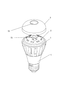
Figure 1 is an overall structure diagram of an LED lighting device according
to a first
embodiment of the invention.
Figure 2 is a cross-sectional structure diagram of the LED lighting device in
Figure 1.
Figure 3 is a schematic diagram of a thermally-conductive surface and a light
distribution
surface of the LED lighting device in Figure 1.
Figure 4 is an overall structure diagram of an LED lighting device according
to a second
embodiment of the invention.
In the drawings:
1 is abase;
2 is a light-emitting chip;
3 is a lamp shade;
31 is a light distribution surface;
6
CA 02937939 2016-07-26
32 is a thermally-conductive surface;
4 is a power supply chamber;
51 is a first cooling hole;
52 is a second cooling hole.
DETAILED DESCRIPTION OF THE PREFERRED EMBODIMENT
The invention is described in detail as follows with reference to specific
embodiments. The following embodiments will help provide further understanding
of the
invention for those skilled in the art, and not in any way limit the
invention. It shall be
noted that several variants and improvements can be made without departing
from
concept of the invention for those of ordinary skill in the art. All these
fall within the
scope of protection of the invention.
An LED lighting device according to the invention, comprises: a base, a
plurality of light-emitting chips, a circuit coating, a lamp shade and a power
supply
chamber. The lamp shade is made of a thermally-conductive solid material with
good
heat conduction. The light-emitting chips are fixed to the base.The lamp shade
is
disposed on the base, to cover the light-emitting chips; the lamp shade is in
contact with
the base by regarding an inner surface other than a corresponding area (i.e.,
a light
distribution surface 31) of the light-emitting chips as a thermally-conductive
surface, to
achieve the heat dissipation function; the inner surface of the corresponding
area of the
lamp shade and light-emitting chips forms a specific shape of space structure
according to
the design needs, to change the light intensity distribution; wherein, the
thermally-
conductive surface is regarded as a part of the inner surface of the lamp
shade, and can
participate in light distribution by using light reflection and/or refraction;
therefore,
technical solutions using the thermally-conductive surface to participate in
light
distribution also belong to the non-limiting embodiments protected by the
invention.
7
CA 02937939 2016-07-26
An upper surface of the base is curved or in a shape of multi-planar
combination. The base employs a hollow structure to increase air circulation
and enhance
heat dissipation, for example, a first cooling hole is arranged in a middle of
the base, to
increase air circulation and enhance heat dissipation; correspondingly, a
second cooling
hole is arranged in a corresponding position of the lamp shade and the base.
An amount
of the light-emitting chips is more than one.
The lamp shade has a light distribution function, and is made of ceramic,
glass
or other highly thermally-conductive materials with light transmission
performance. The
outer surface of the lamp shade is designed into a specific shape according to
the actual
needs. The base is arranged on the power supply chamber, to realize
independent heat
dissipation. The base can be a metal base coated with an insulating layer, a
ceramic base,
etc.
Embodiment 1
Next, the first embodiment is described in detail with reference to Figure 1
and
Figure 2.
The novel LED lighting device mainly comprises a base 1, twenty two LED
light-emitting chips, a circuit coating and a highly thermally-conductive lamp
shade. The
base is a ceramic base with a curved upper surface. A first cooling hole is
arranged in a
middle of the base. The upper surface of the base (except for the cooling
holes) is directly
coated with circuit coating. The circuit coating is a conductive silver paste.
The light-
emitting chips are directly attached to the base, and communicated with each
other
through the circuit coating. The lamp shade is a solid transparent ceramic,
which is made
of polycrystalline AION. A second cooling hole is arranged in a middle
position of the
lamp shade corresponding to the first cooling hole of the base, to achieve air
circulation.
The inner surface of the lamp shade in contact with the base is a curved
surface
corresponding to a shape of the base . The lamp shade contacts with the base
ldirectly,
and covers the base to package the LED light-emitting chips and circuit
coating inside.
The light distribution surface is arranged on the inner surface corresponding
to the LED
8
CA 02937939 2016-07-26
light-emitting chips, but not adhered to the LED light-emitting chips, so as
to form a light
distribution chamber together with the upper surface of the base. The
thermally-
conductive surface is at least distributed in a central region and an edge
region of the
inner surface of the lamp shade, and completely fits with the upper surface of
the base, to
achieve light transmission and heat dissipation. The base has a completely
hollow
structure to achieve cross ventilation. The power supply chamber made of
ceramic is
integrated with the base, but not communicated with the base 1, to realize
independent
heat dissipation.
Embodiment 2
Next, a second embodiment is described in detail with reference to Figure 4.
The LED lighting device mainly comprises a base, twenty seven LED light-
emitting chips, a circuit coating and a lamp shade. The base 1 is an aluminum
base coated
with an insulating material on the upper surface of a multi-bevel shape. The
upper surface
of the base (except for the cooling holes) is directly coated with circuit
coating. The
circuit coating is conductive silver-palladium alloy slurry. The LED light-
emitting chips
are directly attached to the base, and communicated with each other through
the circuit
coating. The lamp shade is a solid transparent ceramic, which is made of
MgA1204. A
second cooling hole is arranged in a middle position of the lamp shade
corresponding to
the first cooling hole of the base, to achieve air circulation. The inner
surface of the lamp
shade in contact with the base is in a shape of multi-planar combination. The
lamp shade
contacts with the base directly, and covers the base to package the LED light-
emitting
chips and the circuit coating inside. The light distribution surface is
arranged on an inner
surface corresponding to the LED light-emitting chips, but not adhered to the
LED light-
emitting chips, so as to form a light distribution chamber together with the
upper surface
of the base. The thermally-conductive surface is at least distributed in a
central region and
an edge region of the inner surface of the lamp shade, and completely fits
with the upper
surface of the base, to achieve light transmission and heat dissipation. The
base has a
completely hollow structure to achieve cross ventilation. The power supply
chamber is
made of plastic. As an independent structure, the power supply chamber is not
9
CA 02937939 2016-07-26
communicated with the base. The base is connected to the power supply chamber
in
screwing mode, to realize independent heat dissipation respectively. The power
supply
chamber and the base can be connected in clamping mode or other modes.
Specific embodiments of the invention are described above. It shall be
understood that the invention is not limited to the above specific
embodiments, and those
skilled in the art can make different variants and modifications within the
scope of the
claims, and it shall not affect the substance of the invention.