Note: Descriptions are shown in the official language in which they were submitted.
CA 02938139 2016-07-28
Blakes Ref. 13592/00003
POWER ADAPTER, ELECTRONIC EQUIPMENT, BATTERY CHARGING SYSTEM
AND METHOD
TECHNICAL FIELD
[0001] The
disclosure belongs to the technical field of charging and particularly relates
to
a power adapter, an electronic equipment, a battery charging system and a
battery charging
method.
BACKGROUND
[0002] Currently,
a battery of an electronic equipment is charged via its power adapter,
while the power adapter typically charges the battery in a constant voltage
output manner;
however, for a high-storage battery, charging the battery in a constant
voltage output manner may
result in an overlong charging time, and hence the prior art above cannot
realize a quick charge
for battery to reduce the charging time.
= SUMMARY
[0003] The
disclosure aims to provide a battery charging system to solve the problem
that the prior art cannot realize a quick charge for battery to reduce the
charging time.
[0004] An
embodiment of the disclosure is realized as follows. There is provided a power
adapter; the power adapter includes a communication interface and charges via
the
communication interface a battery of an electronic equipment.
[0005] During
charging the battery, the power adapter is configured to: first charge the
battery in a regular charging mode; when an output current value of the power
adapter falls
within a regular current range for a predefined time period, send a quick
charge inquiry
instruction to the electronic equipment; after receiving a quick charge
command sent by the
electronic equipment, adjust an output voltage according to battery voltage
information fed back
by the electronic equipment; and if the output voltage meets a quick charge
voltage requirement
predefined, adjust an output current and the output voltage according to a
quick charge mode so
as to charge the battery.
[0006] The
disclosure further provides an electronic equipment. The electronic
22961551.1
CA 02938139 2016-07-28
Blakes Ref. 13592/00003
equipment includes a communication interface, a charging control module and a
battery. Both the
charging control module and the battery are coupled with the communication
interface of the
power adapter via the communication interface such that the power adapter
communicates with
the charging control module and charges the battery, and the charging control
module is also
coupled with electrodes of the battery so as to detect a voltage of the
battery.
[0007] The charging control module is configured to: judge whether
the battery meets a
quick charge requirement, after receiving a quick charge inquiry instruction
sent by the power
adapter; and send a quick charge command to the power adapter and feedback
battery voltage
information to the power adapter, if the battery meets the quick charge
requirement.
[0008] The disclosure further provides a battery charging system. The
battery charging
system includes the power adapter and the electronic equipment above.
[0009] The disclosure further provides a battery charging method
based on the battery
charging system above,. and the battery charging method includes acts as
follows:
during charging a battery, a power adapter first charges the battery in a
regular charging
mode;
when an output current value of the power adapter is within a regular current
range for a
predefined time period, the power adapter performs a quick charge inquiry
communication with
the charging control module;
after after receiving a quick charge command sent by the charging control
module, the
power adapter adjusts an output voltage according to battery voltage
information fed back by the
charging control module;
when the output voltage meets a quick charge voltage requirement predefined by
the
charging control module, the power adapter adjusts an output current and the
output voltage
according to a quick charge mode so as to charge the battery.
BRIEF DESCRIPTION OF THE DRAWINGS
[0010] Fig. 1 is a topological structure diagram of a battery
charging system provided by
an embodiment of the present disclosure;
[0011] Fig. 2 is a flow chart of a battery charging method based on
the battery charging
system as shown in Fig. 1;
2
22961551.1
CA 02938139 2016-07-28
=
Blakes Ref. 13592/00003
[0012] Fig. 3 is another flow chart of a battery charging method
based on the battery
charging system as shown in Fig. 1;
[0013] Fig. 4 is a partial flow chart of acts included in the battery
charging method as
shown in Fig. 2 and Fig. 3 after act S4;
[0014] Fig. 5 is an example flow chart of act Si in the battery charging
method as shown
in Fig. 2 and Fig. 3;
[0015] Fig. 6 is an example flow chart of act S2 in the battery
charging method as shown
in Fig. 2 and Fig. 3;
[0016] Fig. 7 is an example flow chart of act S3 in the battery
charging method as shown
in Fig. 2 and Fig. 3;
[0017] Fig. 8 is an example flow chart of act S4 in the battery
charging method as shown
in Fig. 2 and Fig. 3;
[0018] Fig. 9 is an example block diagram of a power adapter provided
by an
embodiment of the present disclosure;
[0019] Fig. 10 is an example circuit diagram of the power adapter as shown
in Fig. 9;
[0020] Fig. 11 is an example circuit diagram of a charging control
module in an
electronic equipment; and
[0021] Fig. 12 is another example circuit diagram of a charging
control module in an
electronic equipment.
DETAILED DESCRIPTION
[0022] In order to make the objective, the technical solutions and
the advantages of the
present disclosure more clear, the present disclosure is further described in
details below in
conjunction with the accompanying drawings and embodiments. It should be
understood that the
specific embodiments described herein are only used to explain the present
disclosure, but not
used to limit the present disclosure.
[0023] Fig. 1 shows a topology of a battery charging system provided
by an embodiment
of the present disclosure, and for illustration purposes, only parts related
to the embodiments of
the present disclosure are shown, which will be described in details as
follows.
[0024] The battery charging system provided by an embodiment of the present
disclosure
3
22961551.1
CA 02938139 2016-07-28
B lakes Ref. 13592/00003
includes a power adapter 100 and an electronic equipment 500. The power
adapter 100 includes
a communication interface 10 and charges a battery 300 of the electronic
equipment 500 via the
communication interface 10 thereof. The electronic equipment 500 includes a
communication
interface 20, a charging control module 200 and the battery 300. The charging
control module
200 and the battery 300 are electrically coupled with the communication
interface 10 of the
power adapter 100 via the communication interface 20 of the electronic
equipment 500, such that
the power adapter 100 communicates with the charging control module 200 and
charges the
battery 300. And the charging control module 200 is also coupled with
electrodes of the battery
300 to detect a voltage of the battery 300. Each of the communication
interface 10 of the power
adapter 100 and the communication interface 20 of the electronic equipment may
be a USB
interface, including a common USB interface or a mini-USB interface (i.e.
Micro-USB
interface).
[0025] During charging the battery 300, the power adapter 100 first
charges the battery
300 in a regular charging mode. When an output current value of the power
adapter 100 is within
a regular current range for a predefined time period, the power adapter 100
performs a quick
charge inquiry communication with the charging control module 200; after the
charging control
module 200 sends a quick charge command to the power adapter 100, the power
adapter 100
adjusts an output voltage according to battery voltage information fed back by
the charging
control module 200; and when this output voltage meets a quick charge voltage
requirement
predefined in the charging control module 200, the power adapter 100 adjusts
output current and
the output voltage according to a quick charge mode so as to charge the
battery 300, and the
charging control module 200 simultaneously introduces direct current from the
power adapter
100 to charge the battery 300.
[0026] Based on the battery charging apparatus as shown in Fig. 1, an
embodiment of the
disclosure may further provide a battery charging method, as shown in Fig. 2,
such battery
charging method includes acts as follows.
[0027] In block Si, during charging the battery 300, the power adapter
100 first charges
the battery 300 in a regular charging mode.
[0028] In block S2, when an output current value of the power adapter
100 is within a
regular current range for a predefined time period, the power adapter 100
performs a quick
4
22961551.1
CA 02938139 2016-07-28
Blakes Ref. 13592/00003
charge inquiry communication with the charging control module 200.
[0029] In block S3, after the charging control module 200 sends a
quick charge command
to the power adapter 100, the power adapter 100 adjusts an output voltage
according to battery
voltage information fed back by the charging control module 200.
[0030] In block. S4, if the output voltage of the power adapter 100 meets a
quick charge
voltage requirement predefined in the charging control module 200, the power
adapter 100
adjusts the output current and output voltage according to a quick charge mode
so as to charge
the battery 300, and the charging control module 200 simultaneously introduces
direct current
from the power adapter 100 to charge the battery 300.
[0031] In at least one embodiment, the predefined time period may be 3 S
(seconds), and
the regular current range may be set as [1 A, 4 A].
[0032] In consideration that the output current value of the power
adapter 100 may not be
within the regular current range, as a result, based on the battery charging
method as shown in
Fig. 2, as shown in Fig. 3, after block Si, it further includes acts as
follows.
[0033] In block S5, the power adapter 100 detects and judges the output
current.
[0034] In block S6, when the output current value of the power adapter
100 is less than a
lower limit of current, it is returned to carry out block S5.
[0035] In block S7, when the output current value of the power adapter
100 is more than
an upper limit of current, the power adapter 100 turns off a DC output. In
other words, it can be
judged as output short-circuited at this moment, and as a result, the power
adapter 100 turns off
the DC output to realize the short-circuit protection.
[0036] In this embodiment, the block S6 and the block S7 above are
acts parallel with
block S2 and are applied to respond to circumstances that the output current
value of the power
adapter 100 is less than the lower limit of current and that the output
current value of the power
adapter 100 is more than the upper limit of current, respectively. The lower
limit of current may
be 1A, and the upper limit of current above may be 4 A.
[0037] After carrying out block S2 above, in consideration that the
charging control
module 200 may not send the quick charge command to the power adapter 100
(including
communication failure or the charging control module 200 feeding back a quick
charge rejection
command), as a result, in the battery charging method as shown in Fig. 3,
after block S2, it
5
22961551.1
=
CA 02938139 2016-07-28
Blakes Ref. 13592/00003
further includes acts as follows.
[0038] In block. S8, when the charging control module 200 does not
send a quick charge
command to the power adapter 100, it is returned to carry out block S5.
[0039] It can thus be seen that block S8 is an act parallel with block
S3, that is, if the
charging control module 200 does not instruct the power adapter 100 to enter
into the quick
charge mode, the power adapter 100 continues to detect and judge the output
current.
[0040] As shown in Fig. 3, between block S3 and block S4, the battery
charging method
further includes acts as follows.
[0041] In block S9, the power adapter 100 performs a quick charge
voltage inquiry
communication with the charging control module 200 and feeds back output
voltage information
to the charging control module 200.
[0042] In block S10, the charging control module 200 judges according
to the output
voltage information whether the output voltage of the power adapter 100 meets
the quick charge
voltage requirement predefined.
[0043] In this embodiment, the quick charge voltage requirement above may
be a rated
range of quick charge voltage or a rated value of quick charge voltage. That
is, if the output
voltage of the power adapter 100 is within the rated range of quick charge
voltage or equal to the
rated value of quick charge voltage, the output voltage of the power adapter
100 meets the quick
charge voltage requirement. If the charging control module 200 does not feed
back any signal to
the power adapter 100 after block S10, it means the communication between the
power adapter
100 and the charging .control module 200 fails, and the power adapter 100
requires a reset
operation.
[0044] In addition, in consideration that the output voltage of the
power adapter 100 may
not meet the quick charge voltage requirement predefined in the charging
control module 200, as
shown in Fig. 3, between block S10 and block S4, the method further includes
acts as follows.
[0045] In block S11, when the output voltage of the power adapter 100
does not meet the
quick charge voltage requirement predefined in the charging control module
200, the charging
control module 200 sends a voltage deviation feedback signal to the power
adapter 100.
[0046] In block S12, the power adapter 100 adjusts the output voltage
thereof according
to the voltage deviation feedback signal, and it is returned to carry out
block S10.
6
22961551.1
CA 02938139 2016-07-28
Blakes Ref. 13592/00003
[0047] In at least one embodiment, the voltage deviation feedback
signal includes a low
voltage feedback signal and a high voltage feedback signal. If the voltage is
low, the power
adapter 100 increases the output voltage according to the low voltage feedback
signal, and if the
voltage is high, the power adapter 100 lowers the output voltage according to
the high voltage
feedback signal.
[0048] In addition, as shown in Fig. 3, after block S4, the battery
charging method further
includes acts as follows.
[0049] In block S13, the charging control module 200 detects a voltage
of the battery 300
and judges whether the voltage of the battery 300 is bigger than a quick
charge threshold voltage;
if yes, block S14 is carried out, and if not, it is returned to carry out
block S4.
[0050] In block S14, the charging control module 200 stops introducing
the direct current
from the power adapter 100 to charge the battery 300 and feeds back a quick
charge shutdown
command to the power adapter 100.
[0051] In block S15, the power adapter 100 exits from the quick charge
mode according
to the quick charge shutdown command above, and it is returned to carry out
block Si.
[0052] In the quick charge mode above, in order to judge whether a
circuit impedance
between the power adapter 100 and the charging control module 200 is abnormal,
so as to further
judge whether a coupling (including interface coupling, battery contact and
wires) between the
power adapter 100 and the charging control module 200 is abnormal and to stop
charging to
protect the power adapter 100 and the electronic equipment if it is judged as
abnormal, the
battery charging method further includes the following acts executed
simultaneously with block
S4, as shown in Fig. 4.
[0053] In block S16, the power adapter 100 sends a first electrical
parameter access
request to the charging control module 200, and the charging control module
200 sends a second
electrical parameter acCess request to the power adapter 100.
[0054] In block S17, the charging control module 200 feeds back input
voltage
information and input current information of the electronic equipment to the
power adapter 100
according to the first electrical parameter access request.
[0055] In block S18, the power adapter 100 feeds back output voltage
information and
output current information of the power adapter 100 to the charging control
module 200
7
22961551.1
CA 02938139 2016-07-28
Blakes Ref. 13592/00003
according to the second electrical parameter access request.
[0056] In block S19, the power adapter 100 judges according to the
input voltage
information whether a difference between an input voltage of the electronic
equipment and the
output voltage of the power adapter 100 is bigger than an abnormal voltage
difference threshold
and judges according to the input current information whether a difference
between an input
current of the electronic equipment and the output current of the power
adapter 100 is bigger
than an abnormal current difference; if the difference between the input
voltage of the electronic
equipment and the output voltage of the power adapter 100 is bigger than the
abnormal voltage
difference threshold, and/or if the difference between the input current of
the electronic
equipment and the output current of the power adapter 100 is bigger than the
abnormal current
difference, block S20 is carried out; if the difference between the input
voltage of the electronic
equipment and the output voltage of the power adapter 100 is not bigger than
the abnormal
voltage difference threshold and the difference between the input current of
the electronic
equipment and the output current of the power adapter 100 is not bigger than
the abnormal
.. current difference, block S22 is carried out.
[0057] In blockS20, the power adapter 100 sends a first charging
shutdown instruction to
the charging control module 200, and automatically turns off the DC output.
[0058] In block S21, the charging control module 200 instructs,
according to the first
charging shutdown instruction, the electronic equipment to turn off its
communication interface
20.
[0059] In block S22, the charging control module 200 judges according
to the output
voltage information whether the difference between the input voltage of the
electronic equipment
and the output voltage of the power adapter 100 is bigger than the abnormal
voltage difference
threshold and judges according to the output current information whether the
difference between
the input current of the electronic equipment and the output current of the
power adapter 100 is
bigger than the abnormal current difference; if the difference between the
input voltage of the
electronic equipment and the output voltage of the power adapter 100 is bigger
than the
abnormal voltage difference threshold, and/or if the difference between the
input current of the
electronic equipment and the output current of the power adapter 100 is bigger
than the abnormal
current difference, block S23 is carried out; if the difference between the
input voltage of the
8
22961551.1
CA 02938139 2016-07-28
Blakes Ref. 13592/00003
electronic equipment and the output voltage of the power adapter 100 is not
bigger than the
abnormal voltage difference threshold and the difference between the input
current of the
electronic equipment and the output current of the power adapter 100 is not
bigger than the
abnormal current difference, block S16 is carried out.
[0060] In block S23, the charging control module 200 sends a second
charging shutdown
instruction to the power adapter 100 and instructs the electronic equipment to
turn off its
communication interface 20.
[0061] In block S24, the power adapter 100 turns off the DC output
according to the
second charging shutdown instruction.
[0062] In at least one embodiment, the input voltage information of
equipment and the
input current information of equipment refer to the input voltage information
and the input
current information of the electronic equipment, respectively.
[0063] Furthermore, in block Si as shown in Fig. 2 and Fig. 3 above,
the act of charging
by the power adapter 100 the battery 300 in a regular charging mode includes
the following acts
(as shown in Fig. 5).
[0064] In block S101, the power adapter 100, under a circumstance that
the DC output is
turned off, detects and judges whether a voltage of the communication
interface 10 is bigger than
a voltage threshold; if yes, it is continued to carry out block S101 (it is
indicated that the
charging control module 200 does not yet exit from the quick charge mode at
this moment), and
if not, block S102 is carried out.
[0065] In block S102, the power adapter 100 outputs the direct current
according to a
predefined regular output voltage.
[0066] In this embodiment, in the block S101, detecting the voltage of
the
communication interface 10 of the power adapter 100 is to avoid the situation
that the battery
300 is over-charged since the power adapter 100 continues to carry out quick
charge for the
battery 300 due to the charging control module 200 not exiting from the last
quick charge mode.
The voltage threshold may be 2 V, and the regular output voltage may be set as
5.1 V.
[0067] Furthermore, in block S2 as shown in Fig. 2 and Fig. 3 above,
the act of
performing by the power adapter 100 a quick charge inquiry communication with
the charging
control module 200 includes the following acts (as shown in Fig. 6).
9
=
22961551.1
CA 02938139 2016-07-28
=
Blakes Ref. 13592/00003
[0068] In block S201, the power adapter 100 sends a quick charge
inquiry instruction to
the charging control module 200.
[0069] In block S202, the charging control module 200 judges
according to this quick
charge inquiry instruction whether the voltage of the battery 300 reaches a
quick charge voltage
value; if yes, block S203 is carried out, and if not, block S204 is carried
out.
[0070] In block S203, the charging control module 200 feeds back a
quick charge
command to the power adapter 100.
[0071] In block S204, the charging control module 200 feeds back a
quick charge
rejection command to the power adapter 100.
[0072] Furthermore, in block S3 as shown in Fig. 2 and Fig. 3 above, the
act of adjusting
by the power adapter 100 the output voltage according to the battery voltage
information fed
back from the charging control module 200 includes the following acts (as
shown in Fig. 7).
[0073] In block S301, the power adapter 100 sends a battery voltage
access request to the
charging control module 200 according to the quick charge command sent from
the charging
control module 200.
[0074] In block S302, the charging control module 200 feeds back the
battery voltage
information to the power adapter 100 according to the battery voltage access
request above.
[0075] In block S303, the power adapter 100 adjusts its output
voltage to a setting value
of the quick charge voltage according to the battery voltage information
above.
[0076] In at least one embodiment, the setting value of the quick charge
voltage may be
set as a sum of the battery voltage and a predefined voltage increment (such
as 0.2 V). In
addition, if the charging control module 200 does not respond to the battery
voltage access
request sent from the power adapter 100 in block S302 above, the communication
between the
power adapter 100 and the charging control module 200 fails, and the power
adapter 100 carries
out a reset operation at this moment.
[0077] Furthermore, in block S4 as shown in Fig. 2 and Fig. 3 above,
the act of adjusting
by the power adapter 100 the output current and output voltage according to
the quick charge
mode so as to charge the battery 300 includes the following acts (as shown in
Fig. 8).
[0078] In block.S401, the charging control module 200 feeds back an
entry instruction of
the quick charge mode to the power adapter 100.
22961551.1
CA 02938139 2016-07-28
Blakes Ref. 13592/00003
[0079] In block S402, the power adapter 100 adjusts according to the
entry instruction of
the quick charge mode its output current and output voltage to a quick charge
output current and
a quick charge output voltage, respectively.
[0080] In block S403, the power adapter 100 sends a battery voltage
access request to the
charging control module 200.
[0081] In block S404, the charging control module 200 feeds back the
battery voltage
information to the power adapter 100 according to the battery voltage access
request.
[0082] In block S405, the power adapter 100 judges according to the
battery voltage
information whether a difference between the output voltage of the power
adapter 100 and the
voltage of the battery is bigger than a voltage difference threshold; if yes,
block S406 is carried
out (it is indicated that the circuit impedance between the power adapter 100
and both the
charging control module 200 and the battery 300 is abnormal, and the power
adapter 100 is
required to stop outputting direct current), and if not, block S407 is carried
out.
[0083] In block S406, the power adapter 100 turns off the DC output.
[0084] In block S407, the power adapter 100 adjusts its output current
according to the
battery voltage information, and it is returned to carry out block S403 so as
to cyclically adjust
the output current during the quick charge process of the battery 300, thus
optimizing the quick
charge process of the battery 300 for the purpose of shortening the charging
time.
[0085] In at least one embodiment, the quick charge output current
above may be set as 4
A, the quick charge output voltage may be set as any value between 3.4 V and
4.8 V, and the
voltage difference threshold may be 0.8 V.
[0086] Fig. 9 shows an example block diagram of a power adapter, for
illustration
purpose, only parts related to embodiments of the present disclosure are
shown, which will be
described in details as follows.
[0087] The power adapter 100 includes an EMI filter circuit 101, a high-
voltage rectifier
and filter circuit 102, an isolation transformer 103, an output filter circuit
104 and a voltage
tracking and controlling circuit 105. After the EMI of mains electricity is
filtered by the EMI
filter circuit 101, a rectifying and filtering process is conducted by the
high-voltage rectifier and
filter circuit 102 to output high-voltage direct current. After passing
through the isolation
transformer 103 for an electrical isolation and being outputted to the output
filter circuit 104 to
11
22961551.1
CA 02938139 2016-07-28
Blakes Ref. 13592/00003
be filtered, the high-voltage direct current can be used to charge the
battery. The voltage tracking
and controlling circuit 105 adjusts an output voltage of the isolation
transformer 103 according to
an output voltage of the output filter circuit 104.
[0088] The power adapter 100 further includes a power module 106, a
main control
module 107, a potential regulation module 108, a current detection module 109,
a voltage
detection module 110 and an output switch module 111.
[0089] Please refer to Fig. 9 and Fig. 10, an input terminal of the
power module 106 is
coupled with a secondary terminal of the isolation transformer 103. A power
terminal of the main
control module 107, a power terminal of the potential regulation module 108,
and a power
terminal of the current detection module 109 are jointly coupled with an
output terminal of the
power module 106. Both a high-potential terminal of the main control module
107 and a
high-potential terminal of the potential regulation module 108 are coupled
with a positive output
terminal of the output filter circuit 104. The high-level end of the main
control module 107 is
coupled with the positive output end of the output filter circuit 104 via a
second terminal of a
twentieth resistor R20 (i.e., a DC output terminal of the current detection
module 109). A
potential regulation terminal of the potential regulation module 108 is
coupled with the voltage
tracking and controlling circuit 105. A DC input terminal of the current
detection module 109 is
coupled with the positive output terminal of the output filter circuit 104. A
current-feedback
terminal of the current detection module 109 is coupled with a current
detection terminal of the
main control module 107. A clock output terminal and a data output terminal of
the main control
module 107 are coupled with a clock input terminal and a data input terminal
of the potential
regulation module 108, respectively. A first detection terminal and a second
detection terminal of
the voltage detection module 110 are coupled with the DC output terminal of
the current
detection module 109 and a negative output terminal of the output filter
circuit 104, respectively.
A first output terminal and a second output terminal of the voltage detection
module 110 are
coupled with a first voltage detection terminal and a second voltage detection
terminal of the
main control module 107, respectively. An input terminal of the output switch
module 111 is
coupled with the DC output terminal of the current detection module 109. An
output terminal of
the output switch module 111 is coupled with a third detection terminal of the
voltage detection
module 110. A ground. terminal of the output switch module 111 is coupled with
the negative
12
22961551.1
CA 02938139 2016-07-28
Blakes Ref. 13592/00003
output terminal of the output filter circuit 104, a controlled terminal and a
power terminal of the
output switch module 1.11 are coupled with a switch control terminal of the
main control module
107 and the secondary terminal of the isolation transformer 103, respectively.
And the negative
output terminal of the output filter circuit 104, the output terminal of the
output switch module
111, a first communication terminal and a second communication terminal of the
main control
module 107 are all coupled with the communication interface 10 of the power
adapter 100.
[0090] When the power adapter 190 first charges the battery 300 in a
regular charging
mode, the main control module 107 controls the output switch module 111 to
turn off the DC
output of the power adapter 100. The voltage detection module 110 detects the
output voltage of
the power adapter 100 and feeds back a voltage detection signal to the main
control module 107.
According to the voltage detection signal, the main control module 107 judges
whether the
output voltage of the power adapter 100 is bigger than a voltage threshold; if
yes, the voltage
detection module 110 continues to judge the output voltage of the power
adapter 100; if not, the
main control module 107 controls the output switch module 111 to turn on the
DC output of the
power adapter 100 and drives the voltage tracking and controlling circuit 105
through the
potential regulation module 108 to set the output voltage of the isolation
transformer 103 as a
regular output voltage; the current detection module 109 detects the output
current of the power
adapter 100 and feeds back a current detection signal to the main control
module 107; if the main
control module 107 judges according to the current detection signal that the
output current of the
power adapter 100 is within the regular current range for the predefined time
period, the main
control module 107 performs a quick charge inquiry communication with the
charging control
module 200; after the charging control module 200 sends a quick charge command
to the main
control module 107, the main control module 107 drives, according to the
battery voltage
information fed back from the charging control module 200 and through the
potential regulation
module 108, the voltage tracking and controlling circuit 105 to adjust the
output voltage of the
isolation transformer 103 (i.e., adjusting the output voltage of the power
adapter 100); if the
output voltage of the power adapter 100 meets the quick charge voltage
requirement predefined
in the charging control module 200, through the potential regulation module
108, the main
control module 107 drives the voltage tracking and controlling circuit 105 to
adjust the output
voltage of the isolation transformer 103 so as to enable the power adapter 100
to output direct
13
22961551.1
CA 02938139 2016-07-28
Blakes Ref. 13592/00003
current on the basis of a quick charge output current and a quick charge
output voltage, and the
charging control module 200 simultaneously introduces direct current from the
power adapter
100 for charging the battery 300.
[0091]
In this embodiment, when the power adapter 100 first charges the battery 300
in a
regular charging mode, if the output current value of the power adapter 100 is
less than the lower
limit of current (such a' s 1A), the current detection module 109 continues to
detect the output
current of the power adapter 100 and feed back the current detection signal to
the main control
module 107; if the output current value of the power adapter 100 is more than
the upper limit of
current (such as 4A), the main control module 107 controls the output switch
module 111 to turn
off the DC output of the power adapter 100 to realize short-circuit
protection.
[0092]
During the quick charge inquiry communication performed by the main control
module 107 with the charging control module 200 above, the main control module
107 sends a
quick charge inquiry instruction to the charging control module 200, the
charging control module
200 judges according to the quick charge inquiry instruction whether the
voltage of the battery
300 reaches the quick charge voltage value, if yes, a quick charge command is
fed back to the
main control module 107, and if not, a quick charge rejection command is fed
back to the main
control module 107.
[0093]
During the above process that the main control module 107 drives, according to
the battery voltage information fed back from the charging control module 200
and through the
potential regulation module 108, the voltage tracking and controlling circuit
105 to adjust the
output voltage of the isolation transformer 103, the main control module 107
sends a battery
voltage access request to the charging control module 200 according to the
quick charge
command sent from the charging control module 200, the charging control module
200 feeds
back the battery voltage information to the main control module 107 according
to the battery
voltage access request, according to the battery voltage information and
through the potential
regulation module 108 the main control module 107 drives the voltage tracking
and controlling
circuit 105 to adjust the output voltage of the isolation transformer 103 to
the above setting value
of the quick charge voltage.
[0094]
If the output voltage of the power adapter 100 meets the quick charge voltage
requirement predefined in the charging control module 200 (namely in the rated
range of the
=
14
22961551.1
CA 02938139 2016-07-28
Blakes Ref. 13592/00003
quick charge voltage or equal to the rated value of the quick charge voltage),
the main control
module 107 drives, through the potential regulation module 108, the voltage
tracking and
controlling circuit 105 to adjust the output voltage of the isolation
transformer 103, such that the
power adapter 100 outputs direct current on the basis of the quick charge
output current and
quick charge output voltage, and the process of the charging control module
200 simultaneously
introducing direct current from the power adapter 100 to charge the battery
300 may be as
follows.
[0095] The main control module 107 performs a quick charge voltage
inquiry
communication with the charging control module 200, and the main control
module 107 feeds
back the output voltage information to the charging control module 200; if the
output voltage of
the power adapter 100 is in the rated range of the quick charge voltage or
equal to the rated value
of the quick charge voltage, the charging control module 200 determines that
the output voltage
of the power adapter 100 meets the quick charge voltage requirement predefined
in the charging
control module 200, and feeds back the entry instruction of the quick charge
mode to the main
control module 107; according to the entry instruction of the quick charge
mode and through the
potential regulation module 108, the main control module 107 drives the
voltage tracking and
controlling circuit 105 to adjust the output voltage of the isolation
transformer 103, such that the
power adapter 100 outputs direct current on the basis of the quick charge
output current and
quick charge output voltage, and the charging control module 200
simultaneously introduces
direct current from the power adapter 100 to charge the battery 300. In
addition, if the output
voltage of the power adapter 100 does not meet the quick charge voltage
requirement predefined
in the charging control 'module 200 (namely beyond the rated range of the
quick charge voltage
or unequal to the rated value of the quick charge voltage), the charging
control module 200 sends
the voltage deviation feedback signal to the main control module 107, the main
control module
107 drives, according to the voltage deviation feedback signal and through the
potential
regulation module 108, the voltage tracking and controlling circuit 105 to
adjust the output
voltage of the isolation transformer 103, and then continues to perform a
quick charge voltage
inquiry communication with the charging control module 200. In an embodiment,
the voltage
deviation feedback signal includes the low voltage feedback signal and the
high voltage feedback
signal, if the voltage is low, the main control module 107 drives the voltage
tracking and
22961551.1
CA 02938139 2016-07-28
Blakes Ref. 13592/00003
controlling circuit 105 according to the low voltage feedback signal and
through the potential
regulation module 108 to increase the output voltage of the isolation
transformer 103; if the
voltage is high, the main control module 107 drives the voltage tracking and
controlling circuit
105 according to the high voltage feedback signal and through the potential
regulation module
108 to decrease the output voltage of the isolation transformer 103.
[0096]
Further, the above process that the main control module 107 drives, according
to
the entry instruction of the quick charge mode and through the potential
regulation module 108,
the voltage tracking and controlling circuit 105 to adjust the output voltage
of the isolation
transformer 103 such that the power adapter 100 outputs direct current on the
basis of the quick
charge output current and quick charge output voltage may be as follows.
[0097]
The main control module 107 drives the voltage tracking and controlling
circuit
105 through the potential regulation module 108 to adjust the output voltage
of the isolation
transformer 103, so that the output current and output voltage of the power
adapter 100 are
regulated as the quick charge output current (for example, 4A) and the quick
charge output
voltage (such as any value between 3.4V-4.8V), the main control module 107
acquires battery
voltage information from the charging control module 300 and judges according
to the voltage
detection signal fed back by the voltage detection module 110 whether the
difference between
the output voltage of the power adapter 100 and the voltage of the battery is
more than the
voltage difference threshold (for example, 0.8V); if yes, it indicates that
the circuit impedance
among the power adapter 100 and the charging control module 200 and the
battery 300 is
abnormal, the main control module 107 controls the output switch module 111 to
turn off the DC
output of the power adapter 100, and if not, the main control module 107
drives the voltage
tracking and controlling circuit 105 according to the battery voltage
information and through the
potential regulation module 108 to adjust the output voltage of the isolation
transformer 103 so
as to adjust the output current of the power adapter 100, and continues to
acquire battery voltage
information from the charging control module 300, so as to cyclically adjust
the output current of
the power adapter 100 during the quick charge process of battery 300, thus
optimizing the quick
charge process of battery 300 for the purpose of shortening the charging time.
[0098]
In addition, in the meantime the main control module 107 drives the voltage
tracking and controlling circuit 105 via the potential regulation module 108
to adjust the output
16
=
22961551.1
CA 02938139 2016-07-28
Blakes Ref. 13592/00003
voltage of the isolation transformer 103 such that the power adapter 100
outputs direct current on
the basis of the quick charge output current and quick charge output voltage,
the charging control
module 200 detects the voltage of the battery 300; if the voltage of the
battery 300 is larger than
the quick charge threshold voltage (for example, 4.35V), the charging control
module 200 stops
introducing direct current from the power adapter 100 to charge the battery
300 and feeds back
the quick charge shutdown command to the main control module 107. Then, the
main control
module 107 will exit from the quick charge mode according to the quick charge
shutdown
command and returns to the regular charging mode.
[0099] Fig. 10 shows an example circuit diagram of a power adapter in
the battery
charging system provided by an embodiment of the present disclosure, and for
illustration
purposes, only parts related to embodiments of the present disclosure are
shown, which will be
described in details as follows.
[00100] The power module 106 includes: a first capacitor Cl, a voltage
stabilizing chip
Ul, a second capacitor C2, a first inductor Li, a second inductor L2, a first
diode D1, a second
diode D2, a third capacitor C3, a first resistor RI and a second resistor R2.
[00101] A junction between a first terminal of the first capacitor Cl
and both an input
power pin Vin and an enable pin EN of the voltage stabilizing chip Ul is
configured as the input
terminal of the power module 106. A second terminal of the first capacitor Cl
and a ground pin
GND of the voltage stabilizing chip Ul are jointly grounded. A switch pin SW
of the voltage
stabilizing chip Ul and a first terminal of the second capacitor C2 are
jointly coupled with a first
terminal of the first inductor Li. An internal switch pin BOOTSTRAP of the
voltage stabilizing
chip Ul and a second terminal of the second capacitor C2 are jointly coupled
with a cathode of
the first diode Dl. A feedback voltage pin FB of the voltage stabilizing chip
Ul is coupled with a
first terminal of the first resistor R1 and a first terminal of the second
resistor R2, respectively. A
second terminal of the first inductor Ll and a cathode of the second diode D2
are jointly coupled
with a first terminal of the second inductor L2. A junction, formed by jointly
connecting a second
terminal of the second inductor L2 and an anode of the first diode D1, a
second terminal of the
first resistor R1 and a first terminal of the third capacitor C3, is
configured as the output terminal
of the power module 106. An anode of the second diode D2 and a second terminal
of the second
.. resistor R2 and a second terminal of the third capacitor C3 are jointly
grounded. After using the
17
22961551.1
CA 02938139 2016-07-28
Blakes Ref. 13592/00003
voltage stabilizing chip. Ul as a core to perform a voltage converting process
on a voltage at the
secondary terminal of the isolation transformer 103, the power module 106
outputs voltage of
+3.3V to supply power for the main control module 107, the potential
regulation module 108 and
the current detection module 109. The voltage stabilizing chip Ul can be a
Model MCP16301
buck-type DC/DC converter.
[00102] The main control module 107 includes: a main control chip U2,
a third resistor R3,
a reference voltage chip U3, a fourth resistor R4, a fifth resistor R5, a
fourth capacitor C4, a sixth
resistor R6, a seventh resistor R7, a first NMOS transistor Ql , an eighth
resistor R8, a ninth
resistor R9, a tenth resistor R10, an eleventh resistor R11, a twelfth
resistor R12, a thirteenth
resistor R13 and a fourteenth resistor R14.
[00103] A power pin VDD of the main control chip U2 is configured as
the power
terminal of the main control module 107. A ground pin VSS of the main control
chip U2 is
grounded. A first I/0 pin RAO of the main control chip U2 is suspended. A
first terminal of the
third resistor R3 is coupled with the power pin VDD of the main control chip
U2. A second
terminal of the third resistor R3 and a first terminal of the fourth resistor
R4 are jointly coupled
with a positive electrode CATHODE of the reference voltage chip U3. A negative
electrode
ANODE of the reference voltage chip U3 is grounded. A vacant pin NC of the
reference voltage
chip U3 is suspended. A second terminal of the fourth resistor R4 is coupled
with a second 1./0
pin RA1 of the main control chip U2. A third 1/0 pin RA2 of the main control
chip U2 is
configured as the current detection terminal of the main control module 107. A
fourth 110 pin
RA3 of the main control chip U2 is coupled with a first terminal of the fifth
resistor R5. A second
terminal of the fifth resistor R5 and a first terminal of the fourth capacitor
C4 are jointly coupled
with the power pin VDD of the main control chip U2. A second terminal of the
fourth capacitor
C4 is grounded. A fifth I/0 pin RA4 of the main control chip U2 is configured
as the switch
control terminal of the main control module 107. A sixth 1/0 pin RA5 of the
main control chip
U2 is coupled with a first terminal of the sixth resistor R6. A second
terminal of the sixth resistor
R6 and a grid electrode of the first NMOS transistor Q1 are jointly coupled
with a first terminal
of the seventh resistor R7. A second terminal of the seventh resistor R7 and a
source electrode of
the first NMOS transistor Q1 are jointly grounded. A drain electrode of the
first NMOS transistor
Q1 is coupled with a first terminal of the eighth resistor R8. A second
terminal of the eighth
18
=
22961551.1
CA 02938139 2016-07-28
Blakes Ref. 13592/00003
resistor R8 is configured as the high-potential terminal of the main control
module 107. A
seventh I/0 pin RCO and an eighth I/0 pin RC1 of the main control chip U2 are
configured as
the clock output terminal and the data output terminal of the main control
module 107,
respectively. A tenth I/0 pin RC3 and a ninth I/O pin RC2 of the main control
chip U2 are
configured as the first v.oltage detection terminal and the second voltage
detection terminal of the
main control module 107, respectively. An eleventh I/0 pin RC4 and a twelfth
I/0 pin RC5 of
the main control chip U2 are coupled with a first terminal of the ninth
resistor R9 and a first
terminal of the tenth resistor R10, respectively. A first terminal of the
eleventh resistor R11 and a
first terminal of the twelfth resistor R12 are coupled with a second terminal
of the ninth resistor
R9 and a second terminal of the tenth resistor R10, respectively. A second
terminal of the
eleventh resistor R11 and a second terminal of the twelfth resistor R12 are
jointly grounded. A
first terminal of the thirteenth resistor R13 and a first terminal of the
fourteenth resistor R14 are
coupled with the second terminal of the ninth resistor R9 and the second
terminal of the tenth
resistor R10, respectively. A second terminal of the thirteenth resistor R13
and a second terminal
of the fourteenth resistor R14 are jointly coupled with the power pin VDD of
the main control
chip U2. The second terminal of the ninth resistor R9 and the second terminal
of the tenth
resistor R10 are configured as the first communication terminal and the second
communication
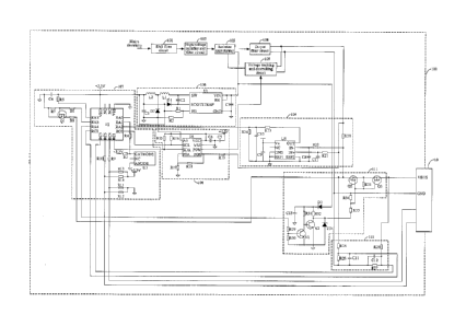
terminal of the main control module 107, respectively. The main control chip
U2 may be a
microcontroller of PIC12LF1822, PIC12F1822, PIC16LF1823 or PIC16F1823 Model,
the
reference voltage chip U3 ,may be the Model LM4040 voltage reference device.
[00104] The potential regulation module 108 includes: A fifteenth
resistor R15, a sixteenth
resistor R16, a digital potentiometer U4, a seventeenth resistor R17, an
eighteenth resistor R18, a
fifth capacitor C5, a sixth capacitor C6 and a nineteenth resistor R19.
[00105] A junction of a first terminal of the fifteenth resistor R15
and a first terminal of
the sixteenth resistor R16, a power pin VDD of the digital potentiometer U4
and a first terminal
of the fifth capacitor C5 is configured as the power terminal of the potential
regulation module
108. A second terminal of the fifth capacitor C5 and a first terminal of the
sixth capacitor C6, a
ground pin VSS of the digital potentiometer U4 and a first terminal of the
seventeenth resistor
R17 are jointly grounded. A second terminal of the sixth capacitor C6 is
coupled with the power
pin VDD of the digital .potentiometer U4. A junction between a second terminal
of the fifteenth
19
22961551.1
CA 02938139 2016-07-28
Blakes Ref. 13592/00003
resistor R15 and a serial data pin SDA of the digital potentiometer U4 is
configured as the data
input terminal of the potential regulation module 108. A junction between a
second terminal of
the sixteenth resistor R16 and a clock input pin SCL of the digital
potentiometer U4 is
configured as the clock input terminal of the potential regulation module 108.
An address zero
pin AO of the digital potentiometer U4 is grounded. A first potential wiring
pin POA of the digital
potentiometer U4 and a first terminal of the eighteenth resistor R18 are
jointly coupled with a
second terminal of the seventeenth resistor R17. A second terminal of the
eighteenth resistor R18
and a second potential wiring pin PUB of the digital potentiometer U4 are
jointly coupled with a
first terminal of the nineteenth resistor R19. A second terminal of the
nineteenth resistor R19 is
configured as the high-potential terminal of the potential regulation module
108, and a potential
tap pin POW of the digital potentiometer U4 is configured as the potential
regulation terminal of
the potential regulation module 108. The digital potentiometer U4 regulates an
internal slide
rheostat according to the clock signal and data signal output by the main
control chip U2,
changing the potential of the tap terminal of the internal slide rheostat,
namely the potential tap
pin POW of the digital potentiometer U4, so that the voltage tracking and
controlling circuit 104
regulates the output voltage of the isolation transformer 103 with the
potential change; the digital
potentiometer U4 may be a MCP45X1 digital potentiometer.
[00106] The current detection module 109 includes: a twentieth resistor
R20, a
twenty-first resistor R21, a twenty-second resistor R22, a seventh capacitor
C7, an eighth
capacitor C8, a current detection chip U5, a twenty-third resistor R23, a
ninth capacitor C9, a
tenth capacitor C10 and a twenty-fourth resistor R24.
[00107] A first terminal and a second terminal of the twentieth
resistor R20 are configured
as the DC input terminal and the DC output terminal of the current detection
module 109,
respectively. A first terminal of the twenty-first resistor R21 and a first
terminal of the
twenty-second resistor R22 are coupled with the first terminal and the second
terminal of the
twentieth resistor R20, respectively. A second terminal of the twenty-first
resistor R21 and a first
terminal of the seventh capacitor C7 are jointly coupled with a positive input
pin IN+ of the
current detection chip U5. A second terminal of the twenty-second resistor R22
and a first
terminal of the eighth capacitor C8 are jointly coupled with a negative input
pin IN- of the
current detection chip U5. A junction between a power pin V+ of the current
detection chip U5
22961551.1
CA 02938139 2016-07-28
Blakes Ref. 13592/00003
=
and a first terminal of the ninth capacitor C9 is configured as the power
terminal of the current
detection module 109. A vacant pin NC of the current detection chip U5 is
suspended. An output
pin OUT of the current detection chip U5 is coupled with a first terminal of
the twenty-third
resistor R23. A second terminal of the twenty-third resistor R23 is configured
as the
current-feedback terminal of the current detection module 109. A first
terminal of the tenth
capacitor C10 and a first terminal of the twenty-fourth resistor R24 are
jointly coupled with the
second terminal of the twenty-third resistor R23. A second terminal of the
seventh capacitor C7,
a second terminal of the eighth capacitor C8, and a second terminal of the
ninth capacitor C9, a
second terminal of the tenth capacitor C10, a second terminal of the twenty-
fourth resistor R24,
and a ground pin GND, a first reference voltage pin REF1 and a second
reference voltage pin
REF2 of the current detection chip U5 are jointly grounded. The twentieth
resistor R20 used as a
current detection resistor samples the output current of the output filter
circuit 104, namely the
output current of the power adapter 100, then the current detection chip U5
outputs a current
detection signal according to the voltage on both ends of the twentieth
resistor R20 to the main
control chip U2. The current detection chip U5 may be an INA286 Model current
shunt monitor.
[00108] The voltage detection module 110 includes: a twenty-fifth
resistor 25, a
twenty-sixth resistor R26, an eleventh capacitor C11, a twelfth capacitor C12,
a twenty-seventh
resistor R27 and a twenty-eighth resistor R28.
[00109] A first terminal of the twenty-fifth resistor R25 is configured
as the first detection
terminal of the voltage detection module 110. A junction between a second
terminal of the
twenty-fifth resistor R25 and both a first terminal of the twenty-sixth
resistor R26 and a first
terminal of the eleventh capacitor C11 is configured as the second output
terminal of the voltage
detection module 110. A second terminal of the twenty-sixth resistor R26 is
configured as the
second detection terminal of the voltage detection module 110. A second
terminal of the eleventh
capacitor C11 and both a first terminal of the twelfth capacitor C12 and a
first terminal of the
twenty-seventh resistor R27 are jointly coupled with the second terminal of
the twenty-sixth
resistor R26. A junction between a second terminal of the twelfth capacitor
C12 and both a
second terminal of the twenty-seventh resistor R27 and a first terminal of the
twenty-eighth
resistor R28 is configured as the first output terminal of the voltage
detection module 110. A
second terminal of the twenty-eighth resistor R28 is configured as the third
detection terminal of
21
22961551.1
CA 02938139 2016-07-28
Blakes Ref. 13592/00003
the voltage detection module 110.
[00110] The output switch module 111 includes: a twenty-ninth resistor
R29, a thirtieth
resistor R30, a thirteenth capacitor C13, a thirty-first resistor R31, a first
NPN-type triode Ni, a
thirty-second resistor R32, a second NPN-type triode N2, a third diode D3, a
voltage stabilizing
diode ZD, a thirty-third resistor R33, a thirty-fourth resistor R34, a thirty-
fifth resistor R35, a
second NMOS transistor Q2 and a third NMOS transistor Q3.
[00111] A first terminal of the twenty-ninth resistor R29 is configured
as the controlled
terminal of the output switch module 111. A second terminal of the twenty-
ninth resistor R29 and
a first terminal of the thirtieth resistor R30 are jointly coupled with a base
electrode of the first
NPN-type triode Ni. A first terminal of the thirteenth capacitor C13 and a
first terminal of the
thirty-first resistor R31, a first terminal of the thirty-second resistor R32
are jointly coupled with
a cathode of the third diode D3. An anode of the third diode D3 is configured
as the power
terminal of the output switch module 111. A second terminal of the thirty-
first resistor R31 and a
base electrode of the second NPN-type triode N2 are jointly coupled with a
collector electrode of
the first NPN-type triode Ni. A second terminal of the thirty-second resistor
R32, a cathode of
the voltage stabilizing diode ZD and a first terminal of the thirty-third
resistor R33 are jointly
coupled with a collector electrode of the second NPN-type triode N2. A second
terminal of the
thirtieth resistor R30, a second terminal of the thirteenth capacitor C13, an
emitter electrode of
the first NPN-type triode Ni, an emitter electrode of the second NPN-type
triode N2 and an
anode of the voltage stabilizing diode ZD are jointly grounded. A second
terminal of the
thirty-third resistor R33 and a first terminal of the thirty-fourth resistor
R34, a first terminal of
the thirty-fifth resistor R35, a grid electrode of the second NMOS transistor
Q2 and a grid
electrode of the third NMOS transistor Q3 are jointly coupled. A second
terminal of the
thirty-fourth resistor R34 is configured as the ground terminal of the output
switch module 111.
A drain electrode of the second NMOS transistor Q2 is configured as the input
terminal of the
output switch module 111. A source electrode of the second NMOS transistor Q2
and a second
terminal of the thirty-fifth resistor R35 are jointly coupled with a source
electrode of the third
NMOS transistor Q3. A drain electrode of the third NMOS transistor Q3 is
configured as the
output terminal of the output switch module 111. The second NMOS transistor Q2
and the third
NMOS transistor Q3 are switched on or off simultaneously to turn on or off the
DC output of the
22
22961551.1
CA 02938139 2016-07-28
Blakes Ref. 13592/00003
=
power adapter 100.
[00112] Fig. 11 shows an example circuit diagram of a charging control
assembly in the
electronic equipment provided by an embodiment of the present disclosure, and
for illustration
purposes, only parts related to embodiments of the present disclosure are
shown, which will be
described in details as follows.
[00113] The = charging control module 200 includes: a battery
connector J1, a main
controller U6, a thirteenth capacitor C13, a thirty-sixth resistor R36, a
thirty-seventh resistor R37,
a fourteenth capacitor C14, a first Schottky diode SD1, a second Schottky
diode SD2, a third
Schottky diode SD3, a fifteenth capacitor C15, a thirty-eighth resistor R38, a
thirty-ninth resistor
R39, a fortieth resistor R40, a third NPN-type triode N3, a fourth NMOS
transistor Q4 and a fifth
NMOS transistor Q5.
[00114] The battery connector Jl is coupled with electrodes of the
battery 300. A first pin
5A-1 and a second pin 5A-2 of the battery connector Jl are jointly grounded. A
first ground pin
GND1 and a second ground pin GND2 of the battery connector J1 are jointly
grounded. A first
1/0 pin RAO of the main controller U6 is coupled with a seventh pin 5A-3 and
an eighth pin
5A-4 of the battery connector Jl respectively. A second 1/0 pin RA1, a seventh
I/0 pin RCO, an
eighth 1/0 pin RC1 and a ninth I/O pin RC2 of the main controller U6 are
coupled with a sixth
pin 2A-4, a fifth pin 2A-3, a fourth pin 2A-2, a third pin 2A-1 of the battery
connector J1,
respectively. Both an analog ground pin VSS and a ground pin GND of the main
controller U6
are grounded. Both a first vacant pin NCO and a second vacant pin NC1 of the
main controller
U6 are suspended. Both a power pin VDD of the main controller U6 and a first
terminal of the
thirteenth capacitor C13 are jointly coupled with the seventh pin 5A-3 and the
eighth pin 5A-4 of
the battery connector J1. A fourth 110 pin RA3 and an eleventh 1/0 pin RC4 of
the main
controller U6 carry out data communications with the electronic equipment. The
thirty-sixth
resistor R36 is coupled between the fourth IJO pin RA3 and the power pin VDD
of the main
controller U6. A sixth I/O pin RA5 and a twelfth I/O pin RC5 of the main
controller U6 are
coupled with the first communication terminal and the second communication
terminal of the
main control module 107 in the power adapter 100, respectively. A first
terminal of the
thirty-seventh resistor R37 and a first terminal of the thirty-eighth resistor
R38 are jointly
coupled with a tenth 1/0 terminal RC3 of the main controller U6. A second
terminal of the
23
22961551.1
CA 02938139 2016-07-28
Blakes Ref. 13592/00003
thirty-seventh resistor R37 is coupled with the power pin VDD of the main
controller U6. A
second terminal of the thirty-eighth resistor R38 is coupled with a base
electrode of the third
NPN-type triode N3. A fifth 1/0 terminal RA4 of the main controller U6 is
coupled with a first
terminal of the fourteenth capacitor C14. A second terminal of the fourteenth
capacitor C14 and a
cathode of the first Schottky diode SD1 are jointly coupled with an anode of
the second Schottky
diode SD2. A first terminal of the thirty-ninth resistor R39 and a first
terminal of the fifteenth
capacitor C15 are jointly coupled with a cathode of the second Schottky diode
SD2. Each of a
second terminal of the thirty-ninth resistor R39, a first terminal of the
fortieth resistor R40 and a
collector electrode of the third NPN-type triode N3 is coupled with a grid
electrode of the fourth
NMOS transistor Q4 and a grid electrode of the fifth NMOS transistor Q5. A
second terminal of
the fortieth resistor R40 and a second terminal of the fifteenth capacitor C15
are jointly grounded.
A source electrode of the fourth NMOS transistor Q4 is coupled with an anode
of the first
Schottky diode SD1, and further coupled with the seventh pin 5A-3 and the
eighth pin 5A-4 of
the battery connector J1. A drain electrode of the fourth NMOS transistor Q4
is coupled with a
drain electrode of the fifth NMOS transistor Q5. A source electrode of the
fifth NMOS transistor
Q5 is coupled with a power wire VBUS of the communication interface 10 of the
power adapter
100. An emitter electrode of the third NPN-type triode N3 is coupled with an
anode of the third
Schottky diode SD3. A cathode of the third Schottky diode SD3 is grounded. The
main controller
U6 may be a microcontroller of PIC12LF1501, PIC12F1501, PIC16LF1503,
PIC16F1503,
PIC16LF1507, PIC16F1507, PIC16LF1508, PIC16F1508, PIC16LF1509 or PIC16F1509
Model.
[00115] When the power adapter 100 operates at the quick charge mode,
the charging
control module 200 introduces direct current from the power adapter 100 to
charge the battery
300 as follows, the main controller U6 outputs a control signal via the fifth
I/O pin RA4 thereof
to control the turn-on of the fourth NMOS transistor Q4 and the fifth
transistor Q5, and controls
the turn-off of the third NPN-type triode N3 via the tenth I/0 pin RC3
thereof, thus introducing
direct current from the communication interface 10 of the power adapter 100 to
charge the
battery 300, since the battery 300 itself has obtained direct current from the
power adapter 100,
the direct current introduced by the charging control module 200 may play a
part in the
increasing of charging' current for battery 300, thus realizing a quick charge
for battery 300;
conversely, when the battery 300 needs to be regularly charged, the main
controller U6 outputs
24
22961551.1
=
CA 02938139 2016-07-28
Blakes Ref. 13592/00003
low level through the fifth 1/0 pin RA4 thereof to control the turn-off of the
fourth NMOS
transistor Q4 and the fifth NMOS transistor Q5, and outputs high level through
the tenth 1/0 pin
RC3 thereof to control the turn-on of the third NPN-type transistor N3.
[00116] The main controller U6 performs data communication via the
fourth I/0 pin RA3
and eleventh 1/0 pin RC4 thereof with the electronic equipment, when the power
supply member
of the electronic equipment is the battery 300, in an embodiment, the main
controller U6 may
transmit voltage and electricity quantity information of the battery 300 to
the electronic
equipment (such as mobile phones), and also the main controller U6 may judge
based on the
voltage of the battery 300 whether the battery 300 has completed the quick
charge process, if yes,
a quick charge shutdown command may be fed back to the electronic equipment to
instruct the
electronic equipment to switch the quick charge mode to the regular charging
mode; during the
power adapter 100 charging the battery 300, if the power adapter 100 is
decoupled from the
battery 300 suddenly, the main controller U6 detects, via the battery
connector J1, the voltage of
= the battery 300 and feeds back a charging termination instruction to the
electronic equipment to
instruct the electronic equipment to terminate the charging process for the
battery 300; in
addition, if the electronic equipment may detect the temperature of the
battery 300, and instruct
the main controller U6 at an abnormal temperature to turn off the fourth NMOS
transistor Q4
and the fifth NMOS transistor Q5, to stop the quick charge for the battery
300, meanwhile the
electronic equipment switches the quick charge mode to the regular charging
mode.
[00117] In addition, when the power adapter 100 operates at a quick charge
mode and the
charging control module 200 introduces direct current from the power adapter
100 to charge the
battery 300, if the power wire VBUS and the ground wire GND of the
communication interface
10 of the power adapter 100 are reversely coupled with the power wire VBUS and
ground wire
GND of communication interface 20 of the electronic equipment (that is the
power wire VBUS
and ground wire GND of communication interface 10 of the power adapter 100 are
respectively
coupled with the ground wire of the charging control module 200 and the source
electrode of the
fifth NMOS transistor Q5), direct current will be introduced from the ground
wire of the
charging control module 200, and the source electrode of the fifth NMOS
transistor Q5 is
coupled with ground.
[00118] As shown in Fig. 12, to avoid damage to components, the charging
control
22961551.1
CA 02938139 2016-07-28
=
Blakes Ref. 13592/00003
module 200 further includes a sixth NMOS transistor Q6, a seventh NMOS
transistor Q7 and a
forty-first resistor R41. A source electrode of the sixth NMOS transistor Q6
is coupled with the
source electrode of the fifth NMOS transistor Q5, a drain electrode of the
sixth NMOS transistor
Q6 is coupled with a drain electrode of the seventh NMOS transistor Q7, a
source electrode of
.. the seventh NMOS transistor Q7 is coupled with the collector electrode of
the third NPN-type
triode N3, grid electrodes of both the sixth NMOS transistor Q6 and the
seventh NMOS
transistor Q7 are coupled with a first terminal of the forty-first resistor
R41, and a second
terminal of the forty-first resistor R41 is grounded.
[00119] When the above reversal coupling fault occurs, direct current
is introduced into
the second terminal of the forty-first resistor R41 from the ground to drive
the turn-off of the
sixth NMOS transistor Q6 and the seventh NMOS transistor Q7, so that the
direct current from
the ground into the charging control module 200 cannot form a loop, thus
preventing the
components in the charging control module 200 from being damaged.
[00120] In conclusion, the embodiments of the present disclosure adopts
a battery
charging system which includes a power adapter 100 and a charging control
module 200; during
charging the battery 300, the power adapter 100 first charges the battery in a
regular charging
mode; when the output current value of the power adapter is within the regular
current range for
the predefined time period, the power adapter performs the quick charge
inquiry communication
with the charging control module; after the charging control module sends a
quick charge
command to the power adapter, the power adapter adjusts the output voltage
according to the
battery voltage information fed back by the charging control module; if such
output voltage
meets the quick charge voltage requirement predefined in the charging control
module, the
power adapter adjusts Me output current and output voltage according to the
quick charge mode
so as to charge the battery, and the charging control module simultaneously
introduces direct
current from the power adapter to charge the battery, thus realizing a quick
charge for battery to
reduce the charging time.
[00121] The above descriptions are merely preferred embodiments of the
disclosure, and
not intended to limit the disclosure; any modifications, equivalent
substitutions and
improvements made within the spirit and principles of the disclosure shall
fall in the protection
scope of the disclosure.
26
22961551.1