Note: Descriptions are shown in the official language in which they were submitted.
CA 02939139 2016-08-09
WO 2015/118178 1 PCT/EP2015/052789
AN ELECTRON EMITTER FOR AN X-RAY TUBE
TECHNICAL FIELD
Example embodiments presented herein are directed towards an electron emitter
for an x-
ray tube. The electron emitter comprises a nanostructure coating made of
oxides, nitrides,
silicides, selinides or tellurides. Example embodiments are further directed
towards an x-
ray tube.
BACKGROUND
The emission of electrons from the surface of a conductor is caused by heating
the
conductor to elevated temperatures, the thermionic emission; by shaping the
conductor
into a sharp point and applying a negative voltage, the field emission, or by
applying a
moderate heating to assist the field emission, for example, Schottky emission
(as a matter
of fact, there are more emission mechanisms as well, like photoemission and
gas ion
impact emission). An electron emitter is commonly referred to as a cathode.
The cathode
working under the respective emission modes are called the hot cathode, cold
cathode or
Schottky cathode, respectively. A device that provides electron beams is
called an
electron source or electron gun. The electrons are perhaps the most common
stimulus for
secondary beams.
The x-ray is generated by the bombardment of energetic electrons on a metal
surface. In this setting, an x-ray source is a device comprising 1) a cathode
and 2) an
electron receiver known as the target or anode. The anode is the x-ray
emitter. The
cathode and the anode are arranged in a particular configuration, and are
enclosed in a
vacuum housing. Moreover, an x-ray system may comprise the following
components, 1)
the x-ray source, 2) the computerized manipulation and handling device, 3) the
detectors
and 4) the power unit(s). In combination with other technologies, x-ray finds
applications
in medical imaging, security inspection, and nondestructive testing in
industry. Computer
technology has revolutionized the use of x-ray in modern society, for example,
x-ray CT
scanner (computed tomography). The advancement in detector technology allowed
improved energy resolution, digital images, and continuously-increasing scan
rates and
areas. On contrary, the technology on the electron source for generating x-
rays remains
essentially the same since the birth of the Coolidge tube for about 100 years
ago, when
CA 02939139 2016-08-09
WO 2015/118178 2 PCT/EP2015/052789
William Coolidge revolutionized the way X-ray was generated by replacing the
gas-filled
tubes with an evacuated tube housing a hot tungsten filament to utilize
thermionic
emission.
SUMMARY
Perhaps all x-ray tubes used in x-ray imaging utilizes hot cathodes of
tungsten
filaments based on thermionic emission. In the past decade or so, attempt was
made to
use carbon nanotubes (CNTs) as cold cathode to generate X-rays by means of
field
emission. Such electron emission is induced by a high electric field without
heating. CNTs
are thought as an ideal emitter for electrons. However, to use them in x-ray
sources, the
manufacture process and work conditions seem to present severe challenge to
their
material properties. The current output is still well below the level for
practical
applications. Thus, at least one object of the example embodiments presented
herein is to
provide an alternative electron emitter, which may provide for alternate means
of electron
emission to overcome the material and operational disadvantages inherent in
the hot
cathodes as well as in the cold cathode based on CNTs; and at the same time
brings in
improved performance of the x-ray sources.
Accordingly, the example embodiments presented herein are directed towards an
electron emitter for x-ray device. The electron emitter comprises a
nanostructure material
made of oxides, nitrides, silicides, selinides or tellurides. Such a
nanostructure material
makes the electron emitter suitable for field emission and more importantly
for Schottky
emission. The use of a thermally assisted electron emission allows for
compensation in
the properties of the hot and cold cathodes. The benefit of the example
embodiments will
be clear, when the comparisons are made between the Schottky emission, the
thermionic
emission, and the field emission. It is well known that a cold cathode can be
poisoned by
the adsorption of electronegative elements such as S, Cl existing as residual
gaseous
species in the tube. If the adsorption is severe, the cathode will cease to
emit electrons.
For a field emission X-ray tube, the cold cathode can be regenerated by
removing the
tube from the housing and baking out the entire tube in an oven, and then
mount the tube
back to see the effect of baking out, a cumbersome process. On the other hand,
for a
Schottky emission tube, the heating resulting in a moderate temperature rise
at the
cathode assists the emission of the electrons while at the same time
preventing the
adsorption of the poisoning gas atoms or molecules on the cathode. In case the
poisoning
occurs, the regeneration can be done by heating the cathode directly without
removing
the tube from the tube housing. The lower power consumption will result in a
more
CA 02939139 2016-08-09
WO 2015/118178 3 PCT/EP2015/052789
compact power source to be utilized, thereby allowing for the x-ray device to
become
more portable. Furthermore, the use of such electron emission mode eliminates
the need
for a cooling system or long cool down and warm up periods which are common
for hot
filament-based systems.
The example embodiments are directed towards an electron emitter for an x-ray
tube. The electron emitter comprises an electrically conductive substrate and
a
nanostructure material. The nanostructure material is comprised on at least a
portion of
the electrically conductive substrate. The nanostructure material is made of
oxides,
nitrides, silicides, selinides or tellurides.
An example advantage of the above embodiment is that the use of such a
nanostructure material allows for a thermally assisted emission, such as a
Schottky
emission. Thus, a more compact x-ray device may be obtained as compared with
Thermionic emission.
According to some of the example embodiments, the electrically conductive
substrate is made of stainless steel, nickel, nickel based alloys, iron or
iron based alloys.
According to some of the example embodiments, the electrically conductive
substrate is in the shape of a solid cylinder with a circular, polygonal, or
star cross-
section.
An example advantage of the above embodiment is the ability to control the
direction, density, as well as other characteristics, of the electron emission
by varying the
shape of the electron emitter.
According to some of the example embodiments, the nanostructure material is
doped or co-doped with a dopant element comprised in column IA, IIA, IB, IIIA,
VIA, or
VIIA in periodic table of the elements.
According to some of the example embodiments, the nanostructure material is
made of ZnO. It should be appreciated that the nanostructure material may be
made of
iron oxides, gallium nitride or any other related alloys or compounds thereof.
An example advantage of such embodiments is the ability of providing an
alternative
to the CNT based electron emitters. The use of such an alternative provides an
example
benefit of providing an electron emitter which is more compatible with
Schottky based
emission. Carbon based electron emitters are prone to damage at the
temperatures and
reactive gaseous environment of typical tube manufacture process. Whereas ZnO
and
related materials are high in melting temperature and chemically more stable
with equally
attractive field emission performance to CNTs.
CA 02939139 2016-08-09
WO 2015/118178 4 PCT/EP2015/052789
According to some of the example embodiments, the portions of the electrically
conductive substrate which do not comprise the nanostructure material further
comprising
a dielectric layer. According to some of the example embodiments, the
dielectric layer is
Si02.
An example advantage of such embodiments is that ability to control the
electron
emission. The controlling may be in the form of controlling a direction or
density of the
electron emission.
According to some of the example embodiments, the electrically conductive
substrate is attachable to a heating element. An example advantage of such an
embodiment is the ability of providing different electron emission modes, for
example, a
Schottky emission.
According to of the example embodiments, the electron emitter is configured
for
Schottky emission when the heating element is in an on-state and the electron
emitter is
negatively biased. According to some of the example embodiments, the electron
emitter is
configured for field emission when the heating element is in an off-state and
the electron
emitter is negatively biased.
An example advantage of such embodiments is that the electron emitter may be
configured for dual operational modes allowing for both field emission and
Schottky based
emission. Furthermore, a hot filament can also be placed. Such an embodiment
has the
example advantage of providing a versatile device utilizing all three electron
emission
modes whenever needed, which may generate x-ray images at various resolutions
and
contrast levels.
Some of the embodiments are directed towards an x-ray device comprising the
electron emitter described above. An example advantage of having such an x-ray
device
is the ability of having a versatile device which may operate in a Schottky
emission mode.
Thus, the device may be portable as described above.
According to some of the example embodiments, the x-ray device further
comprises
a plurality of electron emitters arranged to emit electrons towards an
electron receiving
component. According to some of the example embodiments, the plurality of
electron
emitters is activated individually, simultaneously or sequentially.
Such embodiments have the example advantage of providing a more versatile
device as activating the different electron emitters may provide a difference
in the
resulting electron emission. Thus, differences in image resolution, etc. may
be obtained.
The electron emitters disclosed above with the anode constitutes a so called
diode
X-ray tube. In what follows, the electron source can be configured to consist
of the
CA 02939139 2016-08-09
WO 2015/118178 5 PCT/EP2015/052789
cathode as disclosed above and a grid electrode. And an X-ray source
consisting of this
type of electron source and an anode is referred to as a triode tube.
The example embodiments are directed towards an electron source for X-ray
tube.
The electron source comprises a cathode as disclosed above and a grid, which
are
placed at a fixed interval of distances and fixed by a ceramic spacer. The
grid is made of
electrically conductive wires of equal diameter. Furthermore, the wires are
made of high
melting point, low vapor pressure and electrically conductive materials, such
as W, Mo,
Ta, Ni, stainless steel, or nickel based alloys. The diameter of the wires
varies between 30
um and 150 um. The opening ratio of the grid varies between 50% and 80%.
Furthermore,
the surface of the wires in the grid is coated with a thin layer or
multilayers of material(s)
with properties of pronounced secondary electron emission. Alternatively, the
coating is a
UV emitting material. Thus the coating increases the output intensity of the
electrons from
the source. It is evident, nevertheless better to point out that placing a
grid in front of the
cathode is a common practice in vacuum tubes and even field emission devices,
the
present embodiment exhibits clear distinction to prior art in the following
aspects: the
cathode material, emission mechanism, and an enhancement effect. Thus the
overall
advantages of a this kind of electron source as manifested in a triode X-ray
tube are the
independency of the electron beam on the anode, and the enhanced current
output.
BRIEF DESCRIPTION OF THE DRAWINGS
The foregoing will be apparent from the following more particular description
of the
example embodiments, as illustrated in the accompanying drawings in which like
reference characters refer to the same parts throughout the different views.
The drawings
are not necessarily to scale, emphasis instead being placed upon illustrating
the example
embodiments.
FIG. 1 is a schematic of an x-ray device based on thermionic emission;
FIG. 2 is a schematic of an x-ray, according to the example embodiments
described
herein;
FIG. 3 is an illustrative example of an electron emitter with a grid,
according to some
of the example embodiments described herein;
FIG. 4 is an illustrative example of different shapes an electron emitter may
have,
according to some of the example embodiments described herein;
FIG. 5 is a schematic of an x-ray device comprising multiple electron
emitters,
according to some of the example embodiments described herein; and
CA 02939139 2016-08-09
WO 2015/118178 6 PCT/EP2015/052789
FIGS. 6A and 6B are graphs illustrating the I-V characteristics of the
electron
emitters of FIG. 5, according to some of the example embodiments described
herein.
DETAILED DESCRIPTION
In the following description, for purposes of explanation and not limitation,
specific
details are set forth, such as particular components, elements, techniques,
etc. in order to
provide a thorough understanding of the example embodiments. However, it will
be
apparent to one skilled in the art that the example embodiments may be
practiced in other
manners that depart from these specific details. In other instances, detailed
descriptions
of well-known methods and elements are omitted so as not to obscure the
description of
the example embodiments. The terminology used herein is for the purpose of
describing
the example embodiments and is not intended to limit the embodiments presented
herein.
Example embodiments presented herein are directed towards an electron emitter
for an x-ray device, where the electron emitter comprising a nanostructure
material made
of oxides, nitrides, silicides, selinides or tellurides. Such an electron
emitter is useful for
enabling an x-ray device with a Schottky emission operating mode. In order to
better
describe the example embodiments, a problem will first be identified and
discussed.
Figure 1 illustrates a traditional x-ray tube. The x-ray tube of Figure 1
features an
evacuated glass tube 10 comprising a hot filament cathode 12 and an anode 14
made of
refractory metal/alloy. The surface of the anode 14 faces the cathode 12 at a
predetermined inclination angle. An electric current, provided by a power
supply 13,
passes through the filament cathode 12 causing an increase in the temperature
of the
filament 12 to a level that emits an electron beam 16 from this filament. The
electron
beam 16 is then accelerated towards the anode 14 in the electric field. This
results in an
x-ray beam 18 which is directed out of the device via a window 20. The voltage
difference
between the cathode and the anode determines the energy of the x-ray beam.
Perhaps all x-ray tubes used in X-ray imaging utilizes hot cathodes of
tungsten
filaments based on thermionic emission. In the past decade or so, attempt was
made to
use carbon nanotubes (CNTs) as cold cathode to generate X-rays by means of
field
emission. Such electron emission of is induced by a high electric field
without heating.
CNTs are thought as an ideal emitter for electrons. However, to use them in x-
ray
sources, the manufacture process and work conditions seem to present severe
challenge
to their material properties. The current output is still well below the level
for practical
applications. Thus, at least one object of the example embodiments presented
herein is to
provide an alternative electron emitter, which may provide for alternate means
of electron
CA 02939139 2016-08-09
WO 2015/118178 7 PCT/EP2015/052789
emission to overcome the material and operational disadvantages inherent in
the hot
cathode as well as in the cold cathode based on CNTs; and consequently brings
in
portable x-ray sources with improved performance.
Accordingly, the example embodiments presented herein are directed towards an
electron emitter for x-ray device. The electron emitter comprises a
nanostructure material
made of oxides, nitrides, silicides, selinides or tellurides. Such a
nanostructure material
makes the electron emitter suitable for field emission and more importantly
for Schottky
emission. The use of a thermally assisted electron emission allows for
compensation in
the properties of the hot and cold cathodes. The benefit of the example
embodiments will
be clear, when the comparisons are made between the Schottky emission, the
thermionic
emission, and the field emission. It is well known that a cold cathode can be
poisoned by
the adsorption of electronegative elements such as S, Cl existing as residual
gaseous
species in the tube. If the adsorption is severe, the cathode will cease to
emit electrons.
For a field emission X-ray tube, the cold cathode can be regenerated by
removing the
tube from the housing and baking out the entire tube in an oven, and then
mount the tube
back to see the effect of baking out, cumbersome process. On the other hand,
for a
Schottky emission tube, the heating resulting in a moderate temperature rise
at the
cathode assists the emission of the electrons while at the same time
preventing the
adsorption of the poisoning gas atoms or molecules on the cathode. In case the
poisoning
occur, the regeneration can be done by heating the cathode directly without
removing the
tube from the tube housing. The lower power consumption will result in a more
compact
power source to be utilized, thereby allowing for the x-ray device to become
more
portable. Furthermore, the use of such electron emission mode eliminates the
need for a
cooling system or long cool down and warm up periods which are common for hot
filament-based systems.
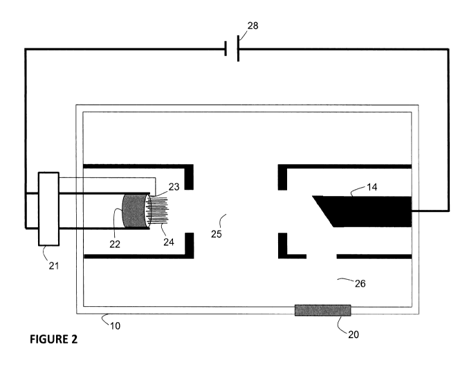
Figure 2 illustrates an x-ray device according to the example embodiments. The
x-
ray device of Figure 2 comprises an evacuated glass tube 10 comprising an
electron
emitter, or cathode, 22 and an electron receiving component 14. The surface of
the
electron receiving component 14 faces the electron emitter 22 at a
predetermined
inclination angle. The plane of the emitters can also be arranged parallel to
the electron
receiving component. An electric current, provided by a power supply 28,
passes through
a heating element 21 causing an increase in the temperature of the electron
emitter 22 to
a level that assist the emission of electrons 25 beam from the electron
emitter 22, when
the cathode at the same time is negatively biased. Such emission is known as
Schottky
emission. In contrast to the electron emission of Figure 1, which is induced
solely by the
CA 02939139 2016-08-09
WO 2015/118178 8 PCT/EP2015/052789
high temperatures due to heating, the emission of Figure 2 is induced by
electric field
under assistance of a moderate heating.
The electrons of electron beam 25 are then accelerated towards the electron
receiving component 14 with an electric field. This results in an x-ray beam
26 which is
directed out of the device via a window 20. The voltage difference between the
electron
emitter and the electron receiving component determines the energy of the x-
ray beam.
According to some of the example embodiments, a grid 30 is placed in between
the
surface 23 comprising the nanostructures 24 of electron emitter and the
electron receiving
component 14 that acts as an extraction electrode, as illustrated in Figure 3.
According to
some of the example embodiments, a spacer 31 is placed between the electron
emitter
and the grid 30. The grid may be placed at an interval distance between 100um
and
1000um which is fixed via the spacer. A circular cover is placed on top of the
grid acting
as the grid electrode providing a voltage to the grid, 32. According to some
of the example
embodiments, the spacer may be a ceramic spacer.
The grid is made of electrically conductive wires of equal diameter.
Furthermore, the
wires are made of high melting point, low vapor pressure and electrically
conductive
materials, such as W, Mo, Ta, Ni, stainless steel, or nickel based alloys. The
diameter of
the wires varies between 30 um and 150 um. The linear opening ratio of the
grid varies
between 50% and 80%. Furthermore, the surface of the wires in the grid is
coated with a
thin layer or multilayers of material(s) with properties of pronounced
secondary electron
emission, such as MgO and related materials. Alternatively, the coating is a
UV emitting
material, such as GaN and related materials.
Thus, the coating increases the output intensity of the electrons from the
electron
emitter. Thus, the overall advantages of a this kind of electron emitter as
manifested in a
triode X-ray tube, as illustrated in Figure 5, are the independency of the
electron beam on
the anode, and the enhanced current output. Furthermore, the field established
between
the electron emitter and the grid determines the intensity of the electron
beam. Again, the
voltage difference between the electron emitter and the electron receiving
component 14
determines the energy of the x-ray beam. It should be appreciated that the
grid and
spacer of Figure 3 may be applied to an electron emitter according to any of
the example
embodiments provided herein.
The electron emitter 22 comprises an electrically conductive substrate 23
comprising of a coating of nanostructures 24. The heating element 21 is
attachable to the
electrically conductive substrate 23 via two electric feed-through at cathode
end of the
tube. The nanostructure coating 24 may be grown on the electrically conductive
substrate
CA 02939139 2016-08-09
WO 2015/118178 9 PCT/EP2015/052789
23. The nanostructure coating may be in the form of nanoparticles, nanowires,
nanorods,
nano tetrapods or nanotubes. The materials of the substrate can be stainless
steel, nickel,
nickel-based alloys, iron or iron-based alloys. According to some of the
example
embodiments, the substrate is pre-formed into various shapes.
Figure 4 illustrates example shapes in which the electron emitter may be
shaped.
The electron emitter 22a is in the shape of a rounded pyramid comprising an
electrically
conductive substrate 23a and a coating of nanostructures 24a. A further
example of an
electron emitter 22b is provided in the form of a solid cylinder also
comprising an
electrically conductive substrate 23b and a coating of nanostructures 24b.
Figure 4
provides a further example of an electron emitter in the form of a hollow
cylinder 22c
featuring an electrically conductive substrate 23c and a coating of
nanostructures 24c. An
additional example of an electron emitter is provided in the form of a hollow
star 22d
comprising an electrically conductive substrate 23d and a coating of
nanostructures 24d.
It should be appreciated that such shapes may be adapted for different uses of
the x-ray
as the shapes may affect the direction of the emitted electrons. It should
further be
appreciated that other shapes may also be employed in the x-ray device
according to the
example embodiments.
The substrates described in Figure 4 may be bundled in parallel at a given
space.
The surface formed by the top ends of the substrates may be planar, concave or
convex
in shape to shape the focal spot of the electron beam.
According to some of the example embodiments, the nanostructure coating may be
grown by a solid-liquid-gas phase method, chemical vapour deposition (CVD)
process, or
a chemical solution method. According to some of the example embodiments, the
nanostructure coating is configured to be altered, with respect to morphology,
to further
facilitate the electron emission by chemical, electrochemical or optical means
in or after
the growth process.
According to some of the example embodiments, the nanostructure coating may be
made of oxides, nitrides, silicides, selinides or tellurides. According to
some of the
example embodiments, the nanostructure coating may be made of oxide
semiconductors,
for example, ZnO. ZnO is an n-type, wide band gap semiconductor. The
conductivity is
associated with the oxygen vacancy generated in the growth process.
Improvement on the conductivity is achieved by doping the chemical elements in
the
columns IA, IIA, IB, IIIA, VIA, VIIA in the periodic table of the elements.
Post-growth heat
treatment is applied to homogenize the dopants or to partially segregate them
to the
surface. The morphology of the nanostructure can be altered by chemical or
CA 02939139 2016-08-09
WO 2015/118178 1 0
PCT/EP2015/052789
electrochemical means to achieve local field enhancement. UV treatment may
also be
applied to improve the surface properties. A surface coating may be applied to
the
nanostructures to further enhance the electron emission process through
decreasing the
work function at the surface of the emitter.
According to some of the example embodiments, a dielectric layer, for example,
Si02, may be added on the electrically conductive substrate in areas in which
the coating
of the nanostructures is not present. Such a dielectric coating may be useful
in directing
the electron emission.
When a moderate heating is applied, via the heating element 21, while the
electron
emitter is negatively biased, the electrons are emitted by Schottky emission.
When the
heating is turned off, while the cathode is negatively biased, the electrons
are emitted by
field emission. The added function of heating, which is absent in pre art
field emission x-
ray sources, may also be applied to regenerate the electron emitter by
removing
unwanted adsorbed chemical species from the surface of the emitters in the
case of
cathode poisoning.
According to some of the example embodiments, multiple electron emitters may
be
used in the x-ray device. Figure 5 illustrates an x-ray tube in which multiple
electron
emitters. In this embodiment, three electron emitters 22_1, 22_2 and 22_3 are
assembled
in the enclosed tube 10 with the emitters facing the electron receiving
component 14. The
number and spacing of the electron emitters may vary.
It should be appreciated that any number of electron emitters may be employed
in
the x-ray device according to the example embodiments. It should further be
appreciated
that the electron emitters of Figure 5 may be the electron emitter featured in
any of
Figures 2 thru 4, or an emitter of any other shape. It should also be
appreciated that the
electron emitters need not be identical and may comprise different shapes
and/or
characteristics with respect to one another.
The pattern of the arrangement of the electron emitters may be, but is not
limited to,
linear, circular, rectangle, square, or other polygonal shape. With respect to
the relation to
the electron receiving component 14, the electron emitters 22_1, 22_2 and 22_3
may be
arranged so all of them emit electrons 25a-25c directed to one focal spot on
the electron
receiving component 14, or so that they project a magnified or demagnified
image of the
emission pattern onto the electron receiving component 14.
All these variations are intended to meet the requirement for the dimension
and the
shape of the x-ray beam 26. The electron emitters 22_1, 22_2 and 22_3 may be
activated
collectively or individually, simultaneously or sequentially. Such a flexible
activation
CA 02939139 2016-08-09
WO 2015/118178 11 PCT/EP2015/052789
regime allows a high frequency, pulsing mode for x-ray generation by setting
the output
frequency of the power source and a wide range of dose selection by choosing
the
number of activated electron emitters 22_1, 22_2 and 22_3. The activation of
the electron
emitters 22_1, 22_2 and 22_3 may be controlled by the power supply 28.
The example embodiments presented herein allow for the individual activation
of the
electron emitters 22_1, 22_2 and 22_3, thereby providing a mechanism for
stabilizing
emission current, which is not available in current x-ray systems. It should
be appreciated
that the inhomogeneity in the emission is a serious problem in large area
cathodes or
multi cathodes. This problem stems from the geometrical and physical
inhomogeneity of
the emitters.
In other words, the problem of the emitters described above stems from
material
and processing issues. Therefore, some of the example embodiments are directed
towards an improvement on the growth of the emitter material on the substrate.
According to some of the example embodiments, the existence of the
inhomogeneity among the emitters is also solved at the component level. Such
an
example embodiment is described by taking a three-cathode configuration as
example of
Figure 5.
Figures 6A and 6B illustrates the current and voltage characteristics of the
electron
emitter configuration of Figure 4. In each graph, the plotted points
represented by the
triangular, square and circular symbols represent the voltages and currents
from the
electron emitters 22_1, 22_2 and 22_3, respectively, of Figure 5.
Figure 6A illustrates an application of voltage V, while keeping a same
distance
between the same electron emitter and electron receiving component. Each
electron
emitter 22_1, 22_2 and 22_3, will emit current i1, i2 and i3, respectively. As
shown in the
graph of Figure 6A, the amount of current supplied by the electron emission of
each
electron emitter differs. Although the inhomogeneity may be quantitatively
described by
formally defining the mean square error or root mean square deviation of the
measured
current values of all emitters in question, the graphical difference shown in
Figure 6A is
sufficient to illustrate the point.
If all of the three electron emitters should emit the same current, then
different
voltages v1, v2, and v3 need to be applied to the electron emitters 22_1, 22_2
and 22_3,
respectively, as seen in Figure 6B. The advantageous consequence manifests
itself when
the electron emitters are directed to different focal spots to create a
particular shape of the
x-ray beam. The mechanism provides a spatial homogeneity of the x-ray beam by
providing a constant current at all focal spots. A further advantage is that
when the
CA 02939139 2016-08-09
WO 2015/118178 12 PCT/EP2015/052789
electron emitters are directed towards one focal spot, and biased
sequentially, the
emitters provide an electron emission with temporal homogeneity with a
constant current
over time. In addition, to ensure the stability and homogeneity of the x-ray
emission, a
feedback monitoring circuit may be used to control the electron emission
process.
According to some of the example embodiments, the electrical power source 28
is
further configured to supply a potential difference between the at least one
electron
generating component(s) and the electron receiving component for a diode tube
in three
bias modes, (-,0: cathode negative, anode grounded), (-,+: cathode negative,
anode
positive) and (0,+: cathode grounded, anode positive). The use of such bias
modes is
provided for inducing the Schottky emission or field emission. Thus, an
example
advantage of such an embodiment with lower heating power requirement is the
elimination of a cooling system or long cool down and warm up periods which
are
common for hot filament-based systems. Thus, a more portable x-ray device may
be
obtained.
According to some of the example embodiments, the electrical power source is
configured to operate in DC mode, i.e. constant (-, 0), (-, +), (0, +); pulse
mode, i.e.
square waves with the anode grounded or with the cathode grounded; or AC mode,
i.e. a
sinus wave. An example advantage of providing an electrical power source with
different
modes of operations is the ability of providing a more versatile device. For
example, in
pulse and AC modes, a defined rising time, frequency, duty cycle and pulse
shape of
waveform may be obtained.
It should be appreciated that the x-ray device described herein may be used in
a
number of fields. For example, the x-ray device may be used in a security
scanning
apparatus, for example, as one would find in an airport security check. As the
use of the
heat element and the Schottky emission allows for a more portable device, the
x-ray
device may be easily implemented in such a security system.
A further example use of the x-ray device discussed herein is in medical
scanning
devices such as a computed tomography (CT) scanning apparatus or a C-arm type
scanning apparatus, which may include a mini C-arm apparatus. A further
example use of
the x-ray device described herein is in a geological surveying apparatus.
It should be appreciated that the x-ray device described herein may be used in
any
non-destructive testing apparatus. A few example application of the x-ray
device may be
mammography, veterinary imaging, and X-ray fluorescence spectrometry, etc.
The description of the example embodiments provided herein have been presented
for purposes of illustration. The description is not intended to be exhaustive
or to limit
CA 02939139 2016-08-09
WO 2015/118178 13 PCT/EP2015/052789
example embodiments to the precise form disclosed, and modifications and
variations are
possible in light of the above teachings or may be acquired from practice of
various
alternatives to the provided embodiments. The examples discussed herein were
chosen
and described in order to explain the principles and the nature of various
example
embodiments and its practical application to enable one skilled in the art to
utilize the
example embodiments in various manners and with various modifications as are
suited to
the particular use contemplated. The features of the embodiments described
herein may
be combined in all possible combinations of methods, apparatus, modules,
systems, and
computer program products. It should be appreciated that the example
embodiments
presented herein may be practiced in any combination with each other.
It should be noted that the word "comprising" does not necessarily exclude the
presence of other elements or steps than those listed and the words "a" or
"an" preceding
an element do not exclude the presence of a plurality of such elements. It
should further
be noted that any reference signs do not limit the scope of the claims, that
the example
embodiments may be implemented at least in part by means of both hardware and
software, and that several "means", "units" or "devices" may be represented by
the same
item of hardware.
In the drawings and specification, there have been disclosed exemplary
embodiments. However, many variations and modifications can be made to these
embodiments. Accordingly, although specific terms are employed, they are used
in a
generic and descriptive sense only and not for purposes of limitation, the
scope of the
embodiments being defined by the following claims.